
|
시장보고서
상품코드
2044000
인도의 반도체 실리콘 웨이퍼 시장 : 시장 점유율 분석, 업계 동향 및 통계, 성장 예측(2026-2031년)India Semiconductor Silicon Wafer - Market Share Analysis, Industry Trends & Statistics, Growth Forecasts (2026 - 2031) |
||||||
인도의 반도체 실리콘 웨이퍼 시장 규모는 2025년에 6억 2,532만 평방인치로 평가되었습니다. 2026년에 6억 6,498만 평방인치가 되어, 2031년까지 9억 2,182만 평방인치에 이를 것으로 예측되며, 2026-2031년에 걸쳐 CAGR 6.75%를 나타낼 전망입니다.

인도의 반도체 미션의 다년간의 자본 보조금에 힘입어 수입 의존에서 국내 생산으로의 빠른 전환이 진행되고 있습니다. 구자라트 주와 우타르 프라데시 주에서 새로운 300mm 생산 능력이 가동되기 시작한 것은 구자라트 주와 우타르 프라데시 주가 대량 생산 및 성숙 노드 제조 기지로서의 입지를 확립하고 있음을 보여줍니다. 국내 수요도 이에 따라 증가하고 있으며, 2025년 전자제품 생산액은 11조 3,000억 루피(1,350억 달러)에 달했으며, 스마트폰과 전기자동차 프로그램이 최종 시장 수요를 견고하게 뒷받침하고 있습니다. 인도의 반도체 실리콘 웨이퍼 시장은 아시아태평양 사업 전개에 있어 인도를 리스크 분산 거점으로 삼고 있는 세계 기업들의 진출로 인해 수혜를 받고 있습니다. 사업 수행은 전력의 안정적 공급, 초순수 확보, 제조 장비의 적기 납품에 좌우되며, 이 모든 것들은 정부와 산업의 긴밀한 협력이 필수적입니다.
인도의 반도체 웨이퍼 시장 동향과 인사이트
'인도의 반도체 미션'을 통한 정부 인센티브 제공
인도의 보조금 제도는 제조 설비 투자의 최대 50%를 상환하기 때문에 수십억 달러 규모의 공장 건설을 대차대조표상의 위험에서 자금 조달이 가능한 프로젝트로 전환할 수 있습니다. 타타 일렉트로닉스는 2024년 2월에 승인을 받고 2026년 12월까지 첫 웨이퍼를 납품하는 것을 목표로 하고 있습니다. 이는 34개월의 건설 주기로 세계 표준보다 8-12개월 빠른 것입니다. 마일스톤 연동형 자금 지원은 건설을 앞당길 수 있지만, 사업주에게는 운전자금을 선지급해야 하는 부담이 있기 때문에 자금력이 있는 기업이나 강력한 벤더 파이낸스 파트너를 보유한 기업이 유리합니다. 케인즈 테크놀로지와 같은 중소기업도 130억 루피 규모의 OSAT 공장 건설에 이 제도를 활용하고 있어, 인센티브가 주력 팹 외에도 파급되고 있음을 알 수 있습니다. 2차적인 효과로는 위탁 재고 제공에 적극적인 웨이퍼 공급업체가 우선적으로 진입할 수 있다는 점을 들 수 있습니다. 이는 장비 설치부터 양산 체제로 전환하기까지의 자금 압박을 완화할 수 있는 조건이 되기 때문입니다.
파운더리 스타트업의 급속한 생산능력 확대
타타 일렉트로닉스, HCL-폭스콘, 식셈은 2028년까지 연간 84만 장의 웨이퍼 처리 능력에 도달할 계획이며, 이는 2031년 인도 예측 수요의 약 5분의 1에 해당합니다. 타타는 2026년 하반기, HCL-Foxconn은 2027년, Sikem은 2028년으로 가동 시기를 늦추면 업스트림 실리콘 수요가 평준화되어 공급업체는 공급과잉을 초래하지 않고 생산량을 조절할 수 있습니다. 제조 공정의 폭은 28nm에서 110nm로, 인도의 EMS(전자제품 위탁생산) 부문이 가장 빠르게 성장하고 있는 자동차, 디스플레이, 산업용 칩 부문과 일치합니다. 각 거점에는 교육 아카데미도 함께 운영되고 있지만, 채용 수요의 총합이 국내 반도체 교육 프로그램의 연간 졸업생 수를 초과하고 있어 2027년까지 인력 부족이 발생할 것으로 예측됩니다. 웨이퍼 벤더의 경우, 이러한 건설 러시는 국내 슬라이싱 능력이 자급자족에 도달하기 전에 장기 계약을 체결하기 위해 약 18개월이라는 제한된 기회를 창출하고 있습니다.
막대한 설비투자와 긴 회수기간
300mm 팹 건설에 30억-50억 달러가 소요되며, 인도의 대출 금리가 8.5%에 가까워 대만이나 한국에 비해 가중평균 자본비용에 200-300bp가 추가됩니다. 타타 그룹의 9,152억 6,000만 루피(110억 달러) 규모의 드레라 프로젝트는 첫 수익이 발생하기까지 얼마나 많은 재정적 위험이 따르는지 잘 보여줍니다. 실트로닉이 20억 유로(22억 달러)를 투자한 싱가포르 공장은 수요 둔화로 인해 2025년 적자로 전환되어 생산 확대기에 수익률의 위험성을 부각시켰습니다. 인도 정부는 설비투자의 50%를 보조하고 있지만, 이 보조금은 마일스톤을 달성할 때마다 지급되기 때문에 사업자는 여전히 선투자를 하고 3-5년에 걸쳐 자금을 회수해야 하기 때문에 운영 초기의 유동성이 부족합니다. 웨이퍼 공급업체는 칩이 출하될 때까지 결제를 미루는 VMI(Vendor Managed Inventory)를 제공함으로써 이익을 얻고 있으며, 운전 자금 부담을 줄이는 대신 우선적인 생산량을 확보할 수 있습니다.
부문 분석
2025년 인도의 반도체 실리콘 웨이퍼 시장에서 300mm 카테고리는 출하량의 74.88%를 차지하며 2031년까지 연평균 7.11%씩 성장하여 작은 직경의 웨이퍼보다 빠른 속도로 성장하고 있습니다. 규모의 경제를 통해 300mm 기판은 200mm 웨이퍼 대비 2.25배의 다이 면적을 1.4배의 설비 비용으로 생산할 수 있어, 단위 비용으로 35-40%의 우위를 점할 수 있습니다. 따라서 타타전자와 같은 국내 팹은 300mm용 장비만을 전제로 설계되어 이 부문의 우위를 더욱 강화하고 있습니다. HCL-Foxconn이 2027년 생산을 본격화하면 인도의 반도체 실리콘 웨이퍼 시장의 300mm 기판 수요는 더욱 확대될 것으로 예측됩니다. 한편, 200mm와 150mm는 기존 공정 노드에서 충분한 파워 디바이스 및 MEMS 부문에서 여전히 중요한 역할을 하고 있습니다.
실트로닉이 150mm 이하 생산에서 철수한 데다 전 세계 200mm 생산능력 증설이 수요를 따라잡지 못해 공급이 부족해 인도 바이어들은 대만이나 한국 공급업체와 장기 계약을 맺어야 하는 상황입니다. 따라서 인도의 반도체 실리콘 웨이퍼 시장에서 소구경 제품의 점유율은 절대 수량이 소폭 증가했음에도 불구하고 비중은 감소하고 있습니다. 300mm 리소그래피와 성막장비의 납기가 18-24개월에 달하기 때문에 국내 슬라이스 생산능력이 확대되기까지 단기간 동안 해외 웨이퍼 벤더들은 프리미엄 가격을 책정할 수 있는 상황이 발생했습니다. 부수적인 영향으로는 팹이 모니터 웨이퍼를 재활용하고 300mm와 기존 규격 모두에서 소모품 비용을 절감하기 위해 다경 대응 리클레임 라인이 필요하게 되었습니다.
2025년에는 로직 디바이스가 생산량의 35.61%를 차지했으며, 이는 스마트폰, 산업용 IoT, 자동차용 마이크로컨트롤러 수요를 반영하고 있습니다. 엣지 AI의 워크로드로 인해 로직 다이 사이즈가 세대별로 20-30%씩 확대되고 있어, 출하량이 정체되어도 웨이퍼 시작 수는 증가합니다. 메모리 웨이퍼는 전 세계 재고 수준이 여전히 높기 때문에 단기적으로 성장세가 둔화될 것으로 예상되지만, 구자라트 주에 위치한 마이크론의 새로운 ATMP 공장에서 완성된 모듈이 출하되고 있습니다. 아날로그, 디스크리트, 센서의 각 카테고리는 각각 전문화된 수직 시장에 대응하고 있으며, 다양한 디바이스 구성을 유지함으로써 팹이 단일 부문의 충격으로부터 보호받을 수 있도록 하고 있습니다.
인도의 디바이스 유형별 구성은 가용한 자본과 인력에 따라 28nm에서 110nm까지의 성숙한 노드를 의도적으로 대상으로 하고 있습니다. 이러한 미세 공정의 로직 제조 흐름은 7nm 이하에서 필요한 고NA EUV 장비를 피할 수 있어 감가상각비와 전력 예산을 모두 절감할 수 있습니다. 자동차 파워트레인의 전동화로 인해 고전압 아날로그 및 디스크리트 디바이스 수요가 증가하고 있으며, 스마트팩토리 구축으로 센서의 채용이 확대되고 있습니다. 그 결과, 인도의 반도체 실리콘 웨이퍼 시장에서 로직의 점유율은 2031년까지 40%에 육박할 것으로 예상되며, AI 서버가 여전히 범용 DRAM 공정에서 동작하는 고 대역폭 변형을 채택함에 따라 메모리도 점진적으로 회복될 것으로 예측됩니다.
'인도의 반도체 웨이퍼 시장 보고서'는 웨이퍼 직경(150mm 이하, 200mm, 300mm), 반도체 디바이스 유형(로직, 메모리, 아날로그, 기타), 웨이퍼 유형(프라임 폴리쉬, 에피택셜, 실리콘 온 인슐레이터(SOI), 기타), 최종 사용자(가전, 모바일, 스마트폰, PC, 서버, 기타), 국가별로 구분하여 조사하였습니다. 최종 사용자(가전, 모바일 및 스마트폰, PC 및 서버, 기타), 국가별로 분류되어 있습니다. 시장 예측은 수량(평방인치) 단위로 제공됩니다.
기타 혜택
- 엑셀 형태 시장 예측(ME) 시트
- 3개월간 애널리스트 지원
자주 묻는 질문
목차
제1장 서론
제2장 조사 방법
제3장 주요 요약
제4장 시장 구도
제5장 시장 규모와 성장 예측
제6장 경쟁 구도
제7장 시장 기회와 향후 전망
KTH 26.05.29The India semiconductor silicon wafer market size is projected to be 625.32 million square inches in 2025, 664.98 million square inches in 2026 and reach 921.82 million square inches by 2031, growing at a CAGR of 6.75% from 2026 to 2031.
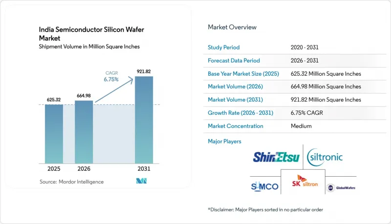
A rapid pivot from import-dependence toward domestic fabrication is underway, underpinned by the India Semiconductor Mission's multi-year capital subsidies. New 300 mm capacity coming online in Gujarat and Uttar Pradesh signals that the country is positioning itself as a high-volume, mature-node manufacturing hub. Domestic demand is rising in tandem: FY25 electronics output touched INR 11.3 lakh crore (USD 135 billion), while smartphone and electric-vehicle programs keep end-market pull robust. The India semiconductor silicon wafer market is also benefiting from the entry of global players that view India as a risk-diversification node in their Asia-Pacific footprint. Even so, execution remains contingent on power reliability, ultra-pure water availability and timely tool deliveries, all of which require tight government-industry coordination.
India Semiconductor Silicon Wafer Market Trends and Insights
Government Incentives Under India Semiconductor Mission
India's subsidy framework reimburses up to 50% of fabrication capex, turning multibillion-dollar plants from balance-sheet risks into financeable projects. Tata Electronics secured approval in February 2024 and aims to deliver the first wafer by December 2026, a 34-month build cycle that is 8 to 12 months quicker than the global norm. Milestone-linked disbursements accelerate construction yet force promoters to fund working capital upfront, favoring firms with deep pockets or strong vendor-financing partners. Smaller players such as Kaynes Technology tapped the same scheme for an INR 13 billion OSAT plant, showing that incentives cascade beyond flagship fabs. A second-order effect is preferential access for wafer suppliers willing to offer consignment inventory, because such terms ease the cash crunch between tool installation and volume ramp.
Rapid Capacity Expansion by Foundry Start-ups
Tata Electronics, HCL-Foxconn, and SicSem together plan to reach 840,000 wafer starts per year by 2028, roughly one-fifth of India's projected 2031 demand. Staggered commissioning, late-2026 for Tata, 2027 for HCL-Foxconn, and 2028 for SicSem, smooths upstream silicon demand, letting suppliers match output without creating gluts. The node mix spans 28 nm to 110 nm, aligning with automotive, display, and industrial chips where India's EMS sector is scaling fastest. Each site also embeds training academies, yet combined hiring needs exceed the annual output of domestic semiconductor programs, foreshadowing a talent squeeze by 2027. For wafer vendors, the build wave creates a finite window, roughly 18 months, to lock long-term agreements before indigenous slicing capacity reaches self-sufficiency.
High Capital Expenditure and Long Payback Periods
Building a 300 mm fab costs USD 3-5 billion, and Indian lending rates near 8.5% add 200-300 basis points to the weighted average cost of capital relative to Taiwan or South Korea. Tata's INR 91,526 crore (USD 11 billion) Dholera project illustrates the scale of financial exposure before first revenue materializes. Siltronic's EUR 2 billion (USD 2.2 billion) Singapore fab turned loss-making in 2025 after demand softened, highlighting margin risk during ramp. Although India reimburses 50% of capex, the subsidy is milestone-based, so promoters still front cash and reclaim funds over three to five years, tightening liquidity in early operations. Wafer suppliers capitalize by offering vendor-managed inventory that defers payment until chips ship, winning priority slots in return for working-capital relief.
Other drivers and restraints analyzed in the detailed report include:
- Rising Domestic Demand for Automotive Power Electronics
- Deployment of 5G Infrastructure Accelerating RF Silicon Consumption
- Limited Ultra-Pure Water and Power Reliability in Fab Clusters
For complete list of drivers and restraints, kindly check the Table Of Contents.
Segment Analysis
The 300 mm category accounted for 74.88% of the 2025 volume in the India semiconductor silicon wafer market and continues to grow faster than smaller diameters, with 7.11% through 2031. Scale economies let a 300 mm substrate yield 2.25 times more die area than a 200 mm wafer, at only 1.4 times the tool cost, translating into a 35-40% unit-cost edge. Domestic fabs such as Tata Electronics are therefore designed exclusively around 300 mm tools, reinforcing this segment's dominance. The India semiconductor silicon wafer market for 300 mm substrates is set to expand further once HCL-Foxconn ramps up in 2027. Conversely, 200 mm and 150 mm remain relevant for power devices and MEMS, where legacy nodes suffice.
Supply-side tightness is emerging because Siltronic has exited <= 150 mm production, and global 200 mm capacity additions trail demand, pushing Indian buyers toward long-term contracts with Taiwanese and Korean suppliers. The India semiconductor silicon wafer market share for smaller diameters, therefore, declines in percentage terms even as absolute volumes inch higher. Equipment lead times of 18-24 months for 300 mm lithography and deposition tools create a brief window during which foreign wafer vendors can command premium pricing before domestic slicing capacity scales up. A secondary effect is the need for multi-diameter reclaim lines, as fabs seek to recycle monitor wafers and shrink consumable costs on both 300 mm and legacy formats.
Logic devices absorbed 35.61% volume in 2025, mirroring smartphone, industrial IoT and automotive microcontroller demand. AI-at-the-edge workloads are lifting logic die sizes 20-30% per generation, so wafer starts rise even if unit shipments plateau. Memory wafers lag in the near term because global inventory remains elevated, although Micron's new ATMP plant in Gujarat ships finished modules. Analog, discrete, and sensor categories each serve specialized verticals, preserving a diversified device mix that cushions fabs against single-segment shocks.
India's device-type split intentionally targets mature nodes, from 28 nm to 110 nm, aligning with available capital and talent. Logic flows at these geometries avoid the high-NA EUV tools required below 7 nm, trimming both depreciation and power budgets. Powertrain electrification in vehicles increases demand for high-voltage analog and discrete devices, while smart-factory buildouts boost sensor adoption. As a result, the India semiconductor silicon wafer market share of logic is expected to edge toward 40% by 2031, with memory recovering gradually as AI servers adopt high-bandwidth variants that still run on commodity DRAM processes.
The India Semiconductor Silicon Wafer Market Report is Segmented by Wafer Diameter (Up To 150 Mm, 200 Mm, and 300 Mm), Semiconductor Device Type (Logic, Memory, Analog, and More), Wafer Type (Prime Polished, Epitaxial, Silicon-On-Insulator (SOI), and More), End-User (Consumer Electronics, Mobile and Smartphones, Pcs and Servers, and More), and Country. The Market Forecasts are Provided in Terms of Volume (Square Inches).
List of Companies Covered in this Report:
- Siltronic AG
- SUMCO Corporation
- Shin-Etsu Chemical Co., Ltd.
- GlobalWafers Co., Ltd.
- SK Siltron Co., Ltd.
- Wafer Works Corporation
- Soitec S.A.
- Okmetic Oy
- GRINM Semiconductor Materials Co., Ltd.
- Hebei China Silicon Corp. (CSC)
- Hangzhou Zhongxin Microelectronics
- Linton Crystal Technologies
- Advanced Technology & Materials Co., Ltd.
- Topsil Semiconductor Materials A/S
- Carl Zeiss SMT GmbH (Wafer Services)
- Vedanta-Foxconn Semiconductors Ltd.
- Tata Electronics Pvt Ltd.
- ISMC Analog Fab Pvt Ltd.
- SCL (Semiconductor Complex Ltd.)
- Bharat Electronics Ltd. (Silicon Foundry)
Additional Benefits:
- The market estimate (ME) sheet in Excel format
- 3 months of analyst support
TABLE OF CONTENTS
1 INTRODUCTION
- 1.1 Study Assumptions and Market Definition
- 1.2 Scope of the Study
2 RESEARCH METHODOLOGY
3 EXECUTIVE SUMMARY
4 MARKET LANDSCAPE
- 4.1 Market Overview
- 4.2 Industry Value-Chain Analysis
- 4.3 Technology Analysis
- 4.4 Regulatory Landscape
- 4.5 Impact of Macroeconomic Factors on the Market
- 4.6 Market Drivers
- 4.6.1 Government Incentives Under India Semiconductor Mission
- 4.6.2 Rapid Capacity Expansion by Foundry Start-ups (Vedanta-Foxconn, Tata Electronics)
- 4.6.3 Rising Domestic Demand for Automotive Power Electronics
- 4.6.4 Deployment of 5G Infrastructure Accelerating RF Silicon Consumption
- 4.6.5 Increasing Shift Toward 300 mm Wafers for Cost Efficiency
- 4.6.6 Growing Outsourcing of Wafer Re-claim and Test Wafers to India
- 4.7 Market Restraints
- 4.7.1 High Capital Expenditure and Long Payback Periods
- 4.7.2 Limited Ultra-Pure Water and Power Reliability in Fab Clusters
- 4.7.3 Shortage of Qualified Process Engineers and Technicians
- 4.7.4 Supply-chain Dependence on Imported Specialty Gases and Chemicals
- 4.8 Porter's Five Forces Analysis
- 4.8.1 Bargaining Power of Suppliers
- 4.8.2 Bargaining Power of Buyers
- 4.8.3 Threat of New Entrants
- 4.8.4 Threat of Substitutes
- 4.8.5 Intensity of Competitive Rivalry
5 MARKET SIZE AND GROWTH FORECASTS (VOLUME)
- 5.1 By Wafer Diameter (Volume, 12-inch-eq. 000 pcs)
- 5.1.1 Up to 150 mm
- 5.1.2 200 mm
- 5.1.3 300 mm
- 5.2 By Semiconductor Device Type
- 5.2.1 Logic
- 5.2.2 Memory
- 5.2.3 Analog
- 5.2.4 Discrete
- 5.2.5 Optoelectronics, Sensors, Micro
- 5.3 By Wafer Type
- 5.3.1 Prime Polished
- 5.3.2 Epitaxial
- 5.3.3 Silicon-on-Insulator (SOI)
- 5.3.4 Specialty Silicon (High-Resistivity, Power, Sensor-Grade)
- 5.4 By End-user
- 5.4.1 Consumer Electronics
- 5.4.2 Mobile and Smartphones
- 5.4.3 PCs and Servers
- 5.4.4 Industrial
- 5.4.5 Telecommunications
- 5.4.6 Automotive
- 5.4.7 Other End-user
6 COMPETITIVE LANDSCAPE
- 6.1 Market Concentration
- 6.2 Strategic Moves
- 6.3 Market Share Analysis
- 6.4 Company Profiles (includes Global Level Overview, Market Level Overview, Core Segments, Financials as available, Strategic Information, Market Rank/Share, Products and Services, Recent Developments)
- 6.4.1 Siltronic AG
- 6.4.2 SUMCO Corporation
- 6.4.3 Shin-Etsu Chemical Co., Ltd.
- 6.4.4 GlobalWafers Co., Ltd.
- 6.4.5 SK Siltron Co., Ltd.
- 6.4.6 Wafer Works Corporation
- 6.4.7 Soitec S.A.
- 6.4.8 Okmetic Oy
- 6.4.9 GRINM Semiconductor Materials Co., Ltd.
- 6.4.10 Hebei China Silicon Corp. (CSC)
- 6.4.11 Hangzhou Zhongxin Microelectronics
- 6.4.12 Linton Crystal Technologies
- 6.4.13 Advanced Technology & Materials Co., Ltd.
- 6.4.14 Topsil Semiconductor Materials A/S
- 6.4.15 Carl Zeiss SMT GmbH (Wafer Services)
- 6.4.16 Vedanta-Foxconn Semiconductors Ltd.
- 6.4.17 Tata Electronics Pvt Ltd.
- 6.4.18 ISMC Analog Fab Pvt Ltd.
- 6.4.19 SCL (Semiconductor Complex Ltd.)
- 6.4.20 Bharat Electronics Ltd. (Silicon Foundry)
7 MARKET OPPORTUNITIES AND FUTURE OUTLOOK
- 7.1 White-Space and Unmet-Need Assessment
