
|
시장보고서
상품코드
1868994
IoT 반도체 설계 및 제조 생태계 시장(2025-2030년)IoT Semiconductor Design and Manufacturing Ecosystem Market Report 2025-2030 |
||||||
이 보고서는 IoT 반도체 설계 및 제조 생태계를 자세히 살펴보고 EDA(Electronic Design Automation) 및 IP(반도체 지적 재산) 시장, 파운드리(제조) 시장을 포함한 시장 규모, 주요 동향 및 시장 점유율을 분석합니다.
샘플 미리보기
세계의 연결된 IoT 디바이스의 설치 대수가 계속 확대되고 있으며, 각 디바이스 내의 반도체 밀도도 그에 따라 증가하고 있습니다. 이 수요의 성장을 지원하는 것은 기반이 되는 칩의 설계와 제조를 담당하는 복잡한 IoT 반도체 밸류 체인입니다.
이 보고서는 설계 및 제조 생태계에 중점을 둔 체계적인 IoT 반도체 밸류체인 분석을 제공합니다. 주요 목표는 밸류체인의 세 가지 기반(EDA, 반도체 IP, 파운드리)을 정의하고 시장 규모를 계산하고 분석함으로써 이 영역을 이해하는 데 도움이 되는 것입니다.
보고서 개요

보고서 개요
- 148페이지의 보고서 : 설계, IP, 제조 생태계에 중점을 둔 IoT 반도체 밸류체인의 종합적인 분석
- 3가지 기술의 딥 다이브 분석 : EDA, 반도체 IP, 파운드리에 대한 상세 분석
- 5개의 반도체의 매크로 트렌드 : AI, 안보, 지정학 등, IoT 반도체 밸류 체인에 영향을 주는 매크로 트렌드의 검증
- 공급업체의 시장 점유율 분석 : EDA, IP, 파운드리의 각 부문에 있어서 경쟁 환경의 내역
- 시장 규모와 예측 : IoT용 EDA, IP, 파운드리 시장의 분석과 예측(-2030년)
주요 분석 영역
- IoT 반도체 개요 : 반도체 구성 요소의 9개 범주를 정의하고 이 보고서에서 분석하는 IoT 반도체 밸류체인의 세 가지 주요 부문에 대해 설명합니다.
- 전체상 - IoT 반도체 시장 : IoT용 반도체 구성 요소 시장 지출 및 설계 및 제조 밸류체인 시장 지출 분석을 제공합니다. 또한 시장 역학에 영향을 미치는 5가지 산업 횡단 동향의 개요를 제시합니다.
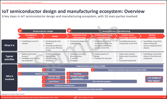
- IoT 반도체 밸류체인 개요 : 설계 및 제조 생태계의 6가지 핵심 단계와 10가지 주요 이해관계자 그룹을 매핑합니다. 부문 및 지역별 시장 지출을 포함하여 4가지 주요 기술 동향을 탐구합니다.
- IoT용 EDA의 상세 분석 : 시스템 사양 책정에서 제조·테스트에 이르는 칩 설계·검증 프로세스를 검증합니다. 지역별 지출 분석, 시장 점유율, 주요 공급업체 프로파일, 4가지 신흥 동향을 제공합니다.
- IoT용 IP 상세 분석 : 반도체 IP의 4대 범주(프로세서, 인터페이스, 메모리, 보안)와 그 하위 부문을 다룹니다. 지역별 시장 규모, 경쟁 구도 평가, 주요 공급업체의 프로파일을 포함합니다.
- IoT용 파운드리의 상세 분석 : 반도체 제조 공정(웨이퍼 준비, 제조, 조립, 테스트, 패키징의 진화)의 개요를 설명합니다. 지역별 지출, 시장 점유율 분석, 주요 파운드리 프로파일을 포함합니다.
게재 기업 :
|
|
|
목차
제1장 주요 요약
제2장 서론
- 장의 개요
- 출발점 : : IoT 접속 디바이스수는 계속 증가하고 있어 2030년에는 390억에 이를 전망
- 각 디바이스 내의 반도체 밀도도 계속 증가하고 있다
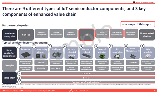
- IoT 반도체 구성 요소에는 9유형가 있으며, 강화된 밸류체인의 주요 구성 요소는 3개
- 정의 : 반도체 및 IoT 반도체
- 정의 : 프로세서
- 정의 : 연결 칩셋
- 정의 : AI 칩셋
- 정의 : 보안 칩셋
- 정의 : 기타
제3장 전체상 : IoT 반도체 시장
- 장의 개요
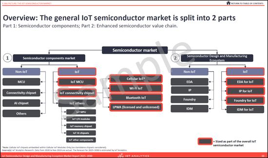
- 개요 : IoT 반도체 시장은 2개의 부분으로 나뉘어져 있습니다.
- 파트 1 : IoT 반도체 구성 요소 - 유형별 지출
- 2부 : IoT 반도체 설계 및 제조 생태계 - 부문별 지출
- IoT 반도체의 전체적인 경쟁 구도
- 여러 반도체 기업에서 IoT 부문의 중요성
- IoT 반도체에 영향을 미치는 5개의 종합적 동향
- 새로운 반도체 공장에 관한 최근 발표
- 조사 방법 : IoT 관련 비즈니스 매핑 - TSMC
IoT 반도체 설계 및 제조 생태계 : 개요
- 장의 개요
- IoT 반도체 설계 및 제조 생태계 : 개요
- IoT 반도체 설계 및 제조 생태계 : 정의
- IoT 반도체 설계 및 제조 시장 지출 - 개요
- IoT 반도체 설계 및 제조에 관한 분석가의 해설
- IoT 반도체 설계 및 제조 시장 지출 - 부문별
- IoT 반도체 설계 및 제조 시장 지출 - 지역별
- 경쟁 구도 : IoT 반도체 설계 및 제조 생태계의 주요 공급업체
- 동향
제5장 IoT용 EDA
- 장의 개요
- IoT 반도체 설계 : 개요
- 칩 설계 및 검증
- PCB 설계 : 프로세스 개요
- 이종 통합 : 개요
- 세계 IoT용 EDA 지출 - 개요(2020-2030년)
- IoT용 EDA에 관한 분석가의 해설
- 세계 IoT용 EDA 지출 예측 - 지역별(2020-2030년)
- 경쟁 구도 : IoT 시장을 위한 EDA의 주요 공급업체
- IoT용 EDA경쟁 구도
- 주요 기업 프로파일 : Cadence
- 주요 기업 프로파일 : Synopsys
- 동향
제6장 IoT용 IP
- 장의 개요
- IoT용 IP
- 세계의 IoT용 IP 지출의 개요(2020-2030년)
- IoT용 IP에 관한 분석가의 해설
- 세계 IoT용 IP 지출 - 지역별(2020-2030년)
- 경쟁 구도 : IoT 시장을 위한 IP의 주요 공급업체
- IoT용 IP경쟁 구도
- 주요 기업 프로파일 : Arm
제7장 IoT용 파운드리
- 장의 개요
- IoT 칩셋용 반도체 제조
- 세계 IoT 지출 개요 : 파운드리(2020-2030년)
- IoT용 파운드리에 관한 분석가의 해설
- 세계의 IoT 지출 : 파운드리 - 지역별(2020-2030년)
- 경쟁 구도 : IoT의 주요 파운드리
- IoT 파운드리경쟁 구도
- 주요 기업 프로파일 : TSMC
제8장 조사 방법과 시장 정의
9장 IoT Analytics 정보
KTH 25.11.26A 148-page report detailing the IoT semiconductor design and manufacturing ecosystem, covering EDA and IP markets as well as foundries, with market sizing, key trends, and market shares.
Sample preview


The global installed base of connected IoT devices continues to expand, driving a corresponding increase in semiconductor density within each device. This growing demand is supported by a complex IoT semiconductor value chain responsible for designing and manufacturing the underlying chips.
This report provides a structured IoT semiconductor value chain analysis, focusing on the design and manufacturing ecosystem. Its primary objective is to help readers understand this landscape by defining, sizing, and analyzing the three foundational pillars of the value chain: Electronic Design Automation (EDA), Semiconductor Intellectual Property (IP), and Foundries.
The findings are based on extensive primary research, including interviews with semiconductor experts from leading vendors and end-user organizations across the IoT semiconductor value chain, complemented by secondary research and insights gathered from major industry trade fairs.
Sample preview


Report at a glance
- 148-page report: A comprehensive analysis of the IoT semiconductor value chain, focusing on the design, IP, and manufacturing ecosystem.
- 3 technology deep dives: In-depth analyses of Electronic Design Automation (EDA), Semiconductor Intellectual Property (IP), and Foundries for IoT.
- 5 overarching semiconductor trends: Examination of macro trends (e.g., AI, security, geopolitics) impacting the IoT semiconductor value chain.
- Vendor market share analysis: A breakdown of the competitive landscape for each of the three ecosystem segments (EDA, IP, and Foundries).
- Market sizing and forecast: Market analysis for the EDA, IP, and Foundry for IoT markets, with forecasts to 2030.
Key areas of analysis
- Introduction to IoT semiconductors: Defines nine categories of semiconductor components and explains the three key segments of the IoT semiconductor value chain analyzed in this report.
- Big picture-The IoT semiconductor market: Provides market spending analysis for both IoT semiconductor components and the design/manufacturing segments of the IoT semiconductor value chain. Also outlines five cross-industry trends influencing market dynamics.
- Overview of the IoT semiconductor value chain: Maps the six critical steps and ten primary stakeholder groups within the design and manufacturing ecosystem. Includes market spending by segment and region and explores four major technical trends.
- EDA for IoT deep dive: Examines the chip design and verification process from system specification to fabrication and testing. Provides regional spending analysis, market share insights, key vendor profiles, and four emerging trends.
- IP for IoT deep dive: Covers the four main types of semiconductor IP (Processor, Interface, Memory, and Security) and their sub-segments. Includes regional market sizing, competitive landscape assessment, and a leading vendor profile.
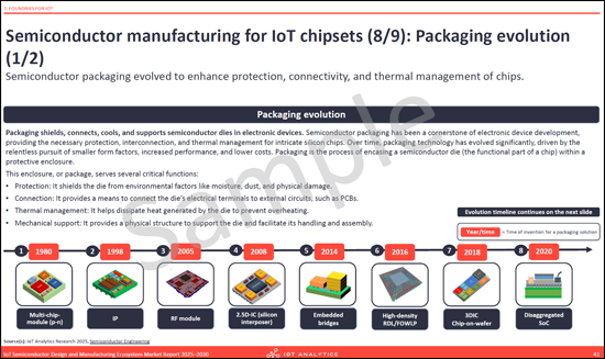
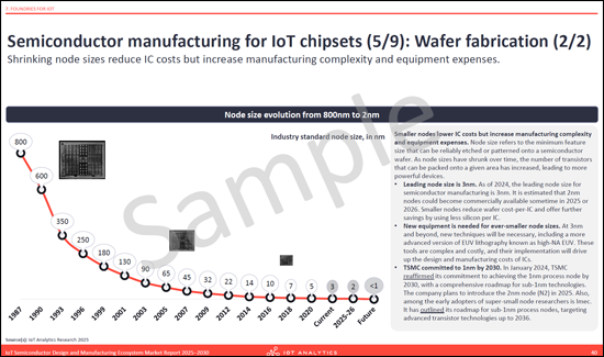
- Foundries for IoT deep dive: Outlines the semiconductor manufacturing process, including wafer preparation, fabrication, assembly, testing, and packaging evolution. Analyzes regional spending, market shares, and includes a leading foundry profile.
A data-driven foundation for key business functions
- Strategy and corporate development: Inform strategic planning with market sizing, 2030 forecasts, and analysis of macro trends impacting the IoT semiconductor value chain, such as geopolitical shifts and supply chain diversification.
- Product management and marketing: Guide product and technology roadmaps using detailed analyses of emerging technology trends and competitive dynamics across the EDA, IP, and foundry segments of the IoT semiconductor value chain.
- R&D and engineering leadership: Direct technical priorities with insights into EDA workflows, IP block architectures, and advanced packaging innovations, along with trends such as security-by-design and cloud-based design platforms.
- Market intelligence and competitive analysis: Benchmark market position within the IoT semiconductor value chain using granular market share data and vendor profiles for the EDA, IP, and foundry segments.
Key concepts defined
- IoT semiconductor value chain: The ecosystem of companies and processes involved in chip creation, defined in this report by six key stages: conception & research, design, integrated circuit manufacturing, printed circuit board manufacturing, surface mount technology assembly, and module assembly.
- Electronic design automation (EDA) for IoT: A key segment of the IoT semiconductor value chain providing software and tools used to design silicon or modules for IoT endpoints or gateways. Includes RTL design, simulation, verification, synthesis, analog/mixed-signal, DFT, advanced packaging, and PCB tools.
- Semiconductor intellectual property (IP) for IoT: A foundational segment of the IoT semiconductor value chain comprising licenses and royalties derived from integrating reusable IP blocks (IP cores) into silicon for IoT devices.
- Foundries for IoT: The manufacturing segment of the IoT semiconductor value chain that provides wafer fabrication and advanced packaging services for chips designed by fabless semiconductor companies.
- Chiplet: A small, specialized IC designed to interconnect with other chiplets or larger ICs. This modular structure enables integration of multiple chips using different process nodes within a single package.
- Heterogeneous integration: A manufacturing approach that combines multiple, separately manufactured components (chips, chiplets, etc.) into a single package, often using different materials and processes.
Questions answered:
- Which stakeholders are involved across EDA, IP, and foundry stages of the value chain?
- Which technologies are critical across EDA, IP, and foundries in enabling IoT semiconductor development?
- What is the current and projected market size of EDA, IP, and foundry for IoT markets?
- What is the market share of leading vendors across these three segments?
- What trends are shaping the future of the IoT semiconductor design and manufacturing ecosystem?
Companies mentioned:
A selection of companies mentioned in the report.
|
|
|
Table of Contents
1. Executive summary
2. Introduction
- Chapter overview: Introduction
- Starting point: The number of loT connected devices continues to grow - Expected to reach 39 billion by 2030
- The semiconductor density within each device also continues to increase
- There are 9 different types of IoT semiconductor components, and 3 key components of enhanced value chain.
- Definitions (1/6): Semiconductors & IoT semiconductors
- Definitions (2/6): Processors
- Definitions (3/6): Connectivity chipsets
- Definitions (4/6): AI chipsets
- Definitions (5/6): Security chipsets
- Definitions (6/6): Other key components
3. Big picture: The IoT semiconductor market
- Chapter overview: Big picture: The IoT semiconductor market
- Overview: The general IoT semiconductor market is split into 2 parts
- Part 1: IoT semiconductor components - Spending by type
- Part 2: IoT semiconductor design and manufacturing ecosystem - Spending by segment
- Overall IoT semiconductor competitive landscape
- Importance of IoT as a segment within several chip companies
- 5 overarching trends impacting IoT semiconductors
- Overarching trend 1
- Overarching trend 2
- Overarching trend 3
- Overarching trend 4
- Overarching trend 5
- Recent announcements for new semiconductor plants
- Methodology: Mapping IoT-related business - TSMC
IoT semiconductor design and manufacturing ecosystem: Overview
- Chapter overview: IoT semiconductor design and manufacturing ecosystem: Overview
- IoT semiconductor design and manufacturing ecosystem: Overview
- IoT semiconductor design and manufacturing ecosystem: Definitions
- IoT semiconductor design and manufacturing market spending - Overview
- Analyst commentary on the IoT semiconductor design and manufacturing
- IoT semiconductor design and manufacturing market spending - By segment
- IoT semiconductor design and manufacturing market spending - By region
- Competitive landscape: Key vendors in IoT semiconductor design and manufacturing ecosystem
- Trend 1
- Trend 2
- Trend 3
- Trend 4
5. EDA for IoT
- Chapter overview: EDA for IoT
- IoT semiconductor design: Overview
- Chip design and verification
- Printed circuit board design: Process overview
- Heterogeneous integration: Overview
- Global EDA for IoT spending 2020-2030 - Overview
- Analyst commentary on the EDA for IoT
- Global EDA for IoT spending 2020-2030 - By region
- Competitive landscape: Key vendors in EDA for IoT market
- EDA for IoT competitive landscape
- Key company profile: Cadence
- Key company profile: Synopsys
- Trend 1
- Trend 2
- Trend 3
- Trend 4
6. IP for IoT
- Chapter overview: IP for IoT
- IP for IoT
- Global IP for IoT spending 2020-2030 - Overview
- Analyst commentary on the IP for IoT
- Global IP for IoT spending 2020-2030 - By region
- Competitive landscape: Key vendors in IP for IoT market
- IP for IoT competitive landscape
- Key company profile: Arm
7. Foundries for IoT
- Chapter overview: Foundries for IoT
- Semiconductor manufacturing for IoT chipsets
- Global Foundry for IoT spending 2020-2030 - Overview
- Analyst commentary on the Foundries for IoT
- Global Foundry for IoT spending 2020-2030 - By region
- Competitive landscape: Key foundries for IoT
- Foundries for IoT competitive landscape
- Key company profile: TSMC
8. Methodology & market definitions
- Key market definitions
- Country mappings to regions
- Research Methodology
