|
시장보고서
상품코드
1936014
스핀 온 카본(SOC) 시장 : 유형별, 용도별, 최종사용자별 - 세계 예측(-2032년)Spin-on Carbon Market by Type (Hot-Temperature, Normal-Temperature), Application (Logic Devices, Memory Devices, Power Devices, MEMS, Photonics, Advanced Packaging), and End User (Foundries, IDMs & OSAT Vendors) - Global Forecast to 2032 |
||||||
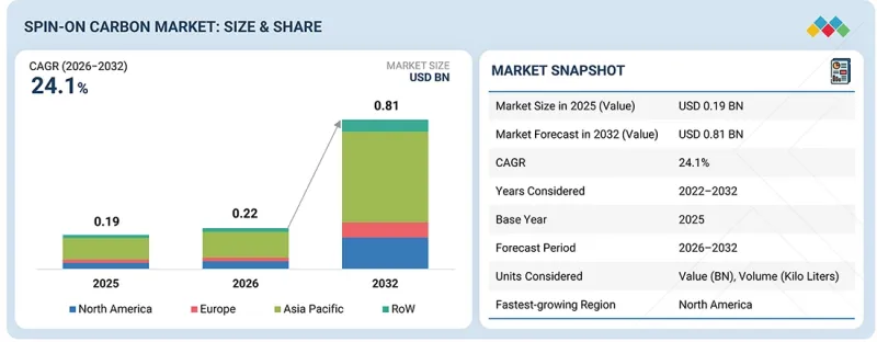
세계의 스핀 온 카본(SOC) 시장 규모는 2026년 2억 2,000만 달러에서 2032년까지 8억 1,000만 달러에 달할 것으로 예측되며, 이 기간에 CAGR로 24.1%의 성장이 전망됩니다.
이러한 성장은 극자외선(EUV) 리소그래피와 심자외선(DUV) 멀티패터닝 기술의 채택 확대에 의해 촉진될 것입니다.
| 조사 범위 | |
|---|---|
| 조사 대상 기간 | 2021-2032년 |
| 기준 연도 | 2024년 |
| 예측 기간 | 2025-2032년 |
| 단위 | 10억 달러 |
| 부문 | 유형, 용도, 최종사용자, 지역 |
| 대상 지역 | 북미, 유럽, 아시아태평양, 기타 지역 |
스핀 온 카본(SOC)은 패턴 전사 성능을 향상시키고, 라인 붕괴를 최소화하며, 대량 생산되는 반도체 제조에서 수율을 향상시킵니다. SOC는 균일한 막 두께와 우수한 기계적 특성을 제공하기 때문에 미세화되는 공정 노드에서 공정 신뢰성을 유지하는 데 필수적입니다.

"최종사용자별로는 파운드리 부문이 2032년 가장 큰 시장 점유율을 차지할 것으로 예측됩니다."
파운드리 부문은 2032년까지 SOC(Spin On Carbon) 시장에서 가장 큰 점유율을 차지할 것으로 예상됩니다. 이는 주로 파운드리가 대규모 반도체 제조에서 중요한 역할을 담당하고 있으며, 첨단 공정 기술이 빠르게 채택되고 있기 때문입니다. TSMC, Samsung Foundry, GlobalFoundries 등 주요 파운드리는 로직, 메모리 인터페이스, AI 가속기, 자동차용 반도체 등 다양한 고객 기반을 확보하고 있습니다. 이러한 광범위한 대응 범위는 다른 최종사용자에 비해 웨이퍼의 시작 횟수를 크게 증가시켜 다양한 리소그래피 레이어 및 에칭 레이어에서 스핀 온 카본(SOC) 재료의 지속적이고 반복적인 소비와 직결됩니다. 또한, 파운드리는 EUV 리소그래피와 복잡한 DUV 멀티패터닝 도입의 최전선에 서 있으며, 첨단 노드에서 패턴 전사 정확도 향상, 라인 붕괴 감소, 수율 향상을 위해 스핀온카본(SOC)이 필수적입니다. 5nm, 3nm와 같은 미세화 노드로의 전환이 진행되는 가운데, 임계 치수의 미세화 및 공정 수 증가로 인해 웨이퍼 당 SOC(Spin-on-Carbon) 사용량은 더욱 증가하고 있습니다. 또한, 파운드리는 CoWoS(Chip-on-Wafer-on-Substrate), INFO(Integrated Fan-Out), 3D 집적 등 첨단 패키징 기술을 강화하고 있습니다. 이러한 공정에서는 평탄화 및 층간 절연 용도로 스핀 온 카본(SOC)이 필수적입니다. 아시아태평양, 북미, 유럽의 지속적인 생산능력 확대는 장기적으로 수요를 증가시킬 것으로 예상됩니다. 그 결과, 파운드리는 2030년까지 스핀온카본(SOC)의 가장 큰 소비 주체가 될 것으로 예상됩니다.
"용도별로는 고급 패키징 부문이 예측 기간 동안 가장 높은 CAGR을 기록할 것으로 예상됩니다."
반도체 제조에서 고밀도 및 이종 집적화로 빠르게 전환함에 따라, 첨단 패키징 부문은 예측 기간 동안 SOC(Spin-on-Carbon) 시장에서 가장 높은 CAGR을 기록할 것으로 예상됩니다. FOWLP(Fan Out Wafer Level Package), 2.5D/3D 집적회로(IC), 칩렛, 실리콘 관통전극(TSV) 등의 기술은 우수한 평탄화, 견고한 층간 접착력, 정밀한 패턴 전사 능력을 필요로 하며, 이는 스핀온카본(SOC) 소재를 통해 실현됩니다.에 의해 실현됩니다. 디바이스 구조가 복잡해짐에 따라 패키지당 스핀온카본(SOC) 사용량이 증가하여 기존 프론트엔드 용도보다 빠른 양산 확대가 예상됩니다. 또한, HPC, AI 가속기, 데이터센터 프로세서에 대한 수요 증가는 트랜지스터 수준의 미세화 한계를 극복하기 위한 첨단 패키징 솔루션의 채택을 촉진하고 있습니다. 스핀 온 카본(SOC) 소재는 미세 피치 상호연결 관리 및 다층 공정에서 결함 감소에 필수적입니다. OSAT 업체에 패키징을 아웃소싱하는 추세도 시장 확대를 뒷받침하고 있으며, 이들 업체는 수율과 처리량 향상을 위해 스핀온 카본(SOC)을 점점 더 많이 활용하고 있습니다. 또한, 높은 신뢰성과 열 안정성이 요구되는 자동차 및 5G 애플리케이션을 위한 패키징 기술의 발전도 스핀온카본(SOC) 소재의 채택을 촉진하고 있습니다.
세계의 스핀 온 카본(SOC) 시장에 대해 조사 분석했으며, 주요 촉진요인 및 저해요인, 제품 개발 및 혁신, 경쟁 구도 등의 정보를 전해드립니다.
자주 묻는 질문
목차
제1장 소개
제2장 주요 요약
제3장 중요한 인사이트
제4장 시장 개요
제5장 업계 동향
제6장 기술의 진보, AI에 의한 영향, 특허, 혁신
제7장 규제 상황
제8장 고객 상황과 구매 행동
제9장 스핀 온 카본(SOC) 시장 : 유형별
제10장 스핀 온 카본(SOC) 시장 : 용도별
제11장 스핀 온 카본(SOC) 시장 : 최종사용자별
제12장 스핀 온 카본(SOC) 시장 : 지역별
제13장 경쟁 구도
제14장 기업 개요
제15장 조사 방법
제16장 부록
KSM 26.03.05The spin-on carbon market is projected to grow from USD 0.22 billion in 2026 to USD 0.81 billion by 2032 at a compound annual growth rate (CAGR) of 24.1% during this period. This growth is driven by the increasing adoption of extreme ultraviolet (EUV) lithography and complex deep ultraviolet (DUV) multi-patterning techniques.
| Scope of the Report | |
|---|---|
| Years Considered for the Study | 2021-2032 |
| Base Year | 2024 |
| Forecast Period | 2025-2032 |
| Units Considered | Value (USD Billion) |
| Segments | By Type, Application, End User and Region |
| Regions covered | North America, Europe, APAC, RoW |
Spin-on carbon (SOC) enhances pattern transfer performance, minimizes line collapse, and improves yield in high-volume semiconductor manufacturing. SOC is essential for maintaining process reliability in increasingly scaled-down nodes, as it provides uniform film thickness and superior mechanical properties.
"By end user, the foundries segment is projected to account for the largest market share in 2032."
The foundries segment is projected to account for the largest market share in the spin-on carbon market by 2032, primarily due to the crucial role of foundries in high-volume semiconductor manufacturing and the rapid adoption of advanced process technologies. Leading foundries like TSMC, Samsung Foundry, and GlobalFoundries cater to a diverse customer base that includes logic, memory interfaces, AI accelerators, and automotive semiconductors. This broad reach results in significantly higher wafer starts than other end users, which directly translates into consistent and recurring consumption of spin-on carbon materials across various lithography and etch layers. Additionally, foundries are at the forefront of implementing EUV lithography and complex DUV multi-patterning, where spin-on carbon is essential for improving pattern transfer fidelity, reducing line collapse, and enhancing yield at advanced nodes. The ongoing migration to smaller nodes, such as 5 nm and 3 nm, further increases spin-on carbon usage per wafer due to tighter critical dimensions and additional processing steps. Moreover, foundries are enhancing their advanced packaging capabilities, including Chip-on-Wafer-on-Substrate (CoWoS), Integrated Fan-Out (InFO), and 3D integration. These processes require spin-on carbon for planarization and interlayer applications. The ongoing capacity expansions across Asia Pacific, North America, and Europe are expected to boost long-term demand. As a result, foundries are projected to become the largest consumers of spin-on carbon by 2030.
"By application, the advanced packaging segment is projected to record the highest CAGR during the forecast period."
The advanced packaging segment is projected to experience the highest compound annual growth rate (CAGR) in the spin-on carbon market during the forecast period due to the rapid transition toward high-density, heterogeneous integration in semiconductor manufacturing. Technologies such as fan-out wafer-level packaging (FOWLP), 2.5D/3D integrated circuits (ICs), chiplets, and through-silicon vias (TSVs) necessitate superior planarization, strong interlayer adhesion, and precise pattern transfer-capabilities made possible by spin-on carbon materials. As device architectures become more complex, the usage of spin-on carbon per package increases, leading to faster volume growth compared to conventional front-end applications. Furthermore, the rising demand for high-performance computing, AI accelerators, and data center processors drives the adoption of advanced packaging solutions to overcome scaling limitations at the transistor level. Spin-on carbon materials are crucial for managing fine-pitch interconnects and reducing defects during multilayer processing. The growing trend of outsourcing packaging to outsourced semiconductor assembly and test (OSAT) companies also supports market expansion, as these vendors increasingly utilize spin-on carbon to enhance yield and throughput. Additionally, advancements in packaging technologies for automotive and 5G applications, which require high reliability and thermal stability, further promote the adoption of spin-on carbon materials.
"North America is projected to grow at the highest CAGR during the forecast period."
North America is projected to experience the highest compound annual growth rate (CAGR) in the spin-on carbon market, driven by increasing investments in domestic semiconductor manufacturing and advanced packaging infrastructure. The region is seeing substantial construction and expansion of semiconductor fabs, motivated by government incentives, reshoring initiatives, and efforts to localize supply chains. Major foundries and integrated device manufacturers (IDMs) are expanding their capacities for advanced-node and specialty processes, which is directly boosting the demand for spin-on carbon materials in various steps, including lithography, etching, and planarization. Furthermore, North America serves as a key center for innovation in extreme ultraviolet (EUV) lithography, artificial intelligence (AI)-focused processors, and high-performance computing-all of which require high-performance spin-on carbon formulations to achieve optimal yield and pattern fidelity at scaled nodes. Additionally, the rapid advancement of packaging technologies, including 2.5D/3D integration and chiplet-based architectures, is leading to an increased consumption of spin-on carbon per wafer and package. Strong collaboration among material suppliers, equipment manufacturers, and semiconductor producers is facilitating a quick qualification and adoption of next-generation spin-on carbon materials. To summarize, the expansion of fabrication capacity, technological leadership, and the rising demand for advanced semiconductor devices position North America as the fastest-growing regional market for spin-on carbon during the forecast period.
Extensive primary interviews were conducted with key industry experts in the spin-on carbon sector to determine and verify the market size for various segments and subsegments, which were gathered through secondary research.
The breakdown of primary participants is provided below.
- By Company Type: Tier 1 - 40%, Tier 2 - 35%, and Tier 3 - 25%
- By Designation: Directors-20%, Managers - 35%, and Others - 45%
- By Region: Asia Pacific - 40%, Europe - 20%, North America - 30%, and RoW - 10%
The report profiles key players in the spin-on carbon market with their respective market ranking analysis. Prominent players profiled in this report are SAMSUNG SDI (South Korea), Shin-Etsu Chemical Co., Ltd. (Japan), DONGJIN SEMICHEM CO LTD. (South Korea), Merck KGaA (Germany), YCCHEM Co., Ltd. (South Korea), Brewer Science, Inc. (US), JSR Micro, Inc. (US), Irresistible Materials (UK), KOYJ CO., LTD. (South Korea), Nano-C (US), among others.
Additionally, SK ecoplant CO., LTD. (South Korea), Pibond Oy (Finland), Qnity Electronics, Inc. (US), Applied Materials, Inc. (US), MicroCHEM (India), Tokyo Electron Limited (Japan), Entegris (US), EV Group (EVG) (Austria), Taiwan Semiconductor Manufacturing Company Limited (Taiwan), GlobalFoundries (US), Intel Corporation (US), among others, are among the few other companies in the spin-on carbon market.
Research Coverage:
This research report categorizes the spin-on carbon market based on type, application, end user, and region. It describes the major drivers, restraints, challenges, and opportunities pertaining to the spin-on carbon market and forecasts the same till 2032. Additionally, the report includes leadership mapping and analysis of all the companies included in the spin-on carbon market ecosystem.
Key Benefits of Buying the Report:
The report will help the market leaders/new entrants in this market with information on the closest approximations of the numbers for the overall spin-on carbon market and the subsegments. It will also help stakeholders understand the competitive landscape and gain more insights to position their businesses better and plan suitable go-to-market strategies. The report will also help stakeholders understand the pulse of the market and provide them with information on key market drivers, restraints, challenges, and opportunities.
The report provides insights into the following pointers:
- Analysis of key drivers (Rapid advancements in semiconductor manufacturing technologies), restraints (Availability of substitute materials), opportunities (Heightened focus on miniaturization of electronic devices), and challenges (Issues selecting suitable SoC materials for integrated circuit manufacturing) of the spin-on carbon market
- Product Development/Innovation: Detailed insights into upcoming technologies, research & development activities, and product & service launches in the spin-on carbon market
- Market Development: Comprehensive information about lucrative markets across varied regions
- Market Diversification: Exhaustive information about new products & services, untapped geographies, recent developments, and investments in the spin-on carbon market
- Competitive Assessment: In-depth assessment of market share, growth strategies, and service offerings of leading players, such as SAMSUNG SDI (South Korea), Shin-Etsu Chemical Co., Ltd. (Japan), DONGJIN SEMICHEM CO LTD. (South Korea), Merck KGaA (Germany), YCCHEM Co., Ltd. (South Korea), in the spin-on carbon market
TABLE OF CONTENTS
1 INTRODUCTION
- 1.1 STUDY OBJECTIVES
- 1.2 MARKET DEFINITION
- 1.3 STUDY SCOPE
- 1.3.1 MARKETS COVERED AND REGIONAL SCOPE
- 1.3.2 INCLUSIONS AND EXCLUSIONS
- 1.3.3 YEARS CONSIDERED
- 1.4 CURRENCY CONSIDERED
- 1.5 UNIT CONSIDERED
- 1.6 LIMITATIONS
- 1.7 STAKEHOLDERS
- 1.8 SUMMARY OF CHANGES
2 EXECUTIVE SUMMARY
- 2.1 MARKET HIGHLIGHTS AND KEY INSIGHTS
- 2.2 KEY MARKET PARTICIPANTS: MAPPING OF STRATEGIC DEVELOPMENTS
- 2.3 DISRUPTIONS SHAPING SPIN-ON CARBON MARKET
- 2.4 HIGH-GROWTH SEGMENTS
- 2.5 SNAPSHOT: GLOBAL MARKET SIZE, GROWTH RATE, AND FORECAST
3 PREMIUM INSIGHTS
- 3.1 ATTRACTIVE OPPORTUNITIES FOR PLAYERS IN SPIN-ON CARBON MARKET
- 3.2 SPIN-ON CARBON MARKET, BY TYPE
- 3.3 SPIN-ON CARBON MARKET, BY APPLICATION
- 3.4 SPIN-ON CARBON MARKET, BY END USER
- 3.5 SPIN-ON CARBON MARKET IN ASIA PACIFIC, BY END USER AND COUNTRY
- 3.6 SPIN-ON CARBON MARKET, BY GEOGRAPHY
4 MARKET OVERVIEW
- 4.1 INTRODUCTION
- 4.2 MARKET DYNAMICS
- 4.2.1 DRIVERS
- 4.2.1.1 Rapid advances in semiconductor manufacturing technologies
- 4.2.1.2 Increasing need for advanced electronic device packaging
- 4.2.1.3 Growing preference for EUV lithography-enabled memory production
- 4.2.1.4 Rising structural complexity of semiconductor devices
- 4.2.2 RESTRAINTS
- 4.2.2.1 Availability of substitute materials
- 4.2.2.2 High sensitivity of SoC materials to process variations
- 4.2.3 OPPORTUNITIES
- 4.2.3.1 Heightened focus on miniaturization of electronic devices
- 4.2.3.2 Requirement for next-generation memory devices in emerging technologies
- 4.2.3.3 Increase in wafer fabrication capacity
- 4.2.4 CHALLENGES
- 4.2.4.1 Issues in selecting suitable SoC materials for integrated circuit manufacturing
- 4.2.4.2 Challenges in scaling SoC materials for next-generation advanced semiconductor nodes
- 4.2.1 DRIVERS
- 4.3 INTERCONNECTED MARKETS AND CROSS-SECTOR OPPORTUNITIES
- 4.4 STRATEGIC MOVES BY TIER 1/2/3 PLAYERS
5 INDUSTRY TRENDS
- 5.1 INTRODUCTION
- 5.2 PORTER'S FIVE FORCES ANALYSIS
- 5.2.1 THREAT OF NEW ENTRANTS
- 5.2.2 THREAT OF SUBSTITUTES
- 5.2.3 BARGAINING POWER OF SUPPLIERS
- 5.2.4 BARGAINING POWER OF BUYERS
- 5.2.5 INTENSITY OF COMPETITIVE RIVALRY
- 5.3 MACROECONOMIC OUTLOOK
- 5.3.1 INTRODUCTION
- 5.3.2 GDP TRENDS AND FORECAST
- 5.3.3 TRENDS IN GLOBAL LITHOGRAPHY INDUSTRY
- 5.3.4 TRENDS IN GLOBAL LOGIC DEVICE INDUSTRY
- 5.4 VALUE CHAIN ANALYSIS
- 5.5 ECOSYSTEM ANALYSIS
- 5.6 PRICING ANALYSIS
- 5.6.1 PRICING RANGE OF SPIN-ON CARBON, BY KEY PLAYER, 2024
- 5.6.2 AVERAGE SELLING PRICE TREND OF SPIN-ON CARBON, BY REGION, 2022-2025
- 5.7 TRADE ANALYSIS
- 5.7.1 IMPORT SCENARIO (HS CODE 381800)
- 5.7.2 EXPORT SCENARIO (HS CODE 381800)
- 5.8 KEY CONFERENCES AND EVENTS, 2026-2027
- 5.9 TRENDS/DISRUPTIONS IMPACTING CUSTOMER BUSINESS
- 5.10 INVESTMENT AND FUNDING SCENARIO, 2023-2025
- 5.11 CASE STUDY ANALYSIS
- 5.11.1 BREWER SCIENCE DEVELOPS HTSOC MATERIALS FOR ADVANCED PATTERN TRANSFER APPLICATIONS
- 5.11.2 IRRESISTIBLE MATERIALS OFFERS SOC MATERIAL TO HELP ACHIEVE HIGH ETCH RESISTANCE AND THERMAL STABILITY OF SEMICONDUCTORS
- 5.11.3 IRRESISTIBLE MATERIALS PROVIDES HIGH-RESOLUTION SOC HARDMASKS TO INTEL CORPORATION TO IMPROVE NANOFABRICATION CAPABILITIES
- 5.12 IMPACT OF 2025 US TARIFF - SPIN-ON CARBON MARKET
- 5.12.1 INTRODUCTION
- 5.12.2 KEY TARIFF RATES
- 5.12.3 PRICE IMPACT ANALYSIS
- 5.12.4 IMPACT OF COUNTRIES/REGIONS
- 5.12.4.1 US
- 5.12.4.2 Europe
- 5.12.4.3 Asia Pacific
- 5.12.5 IMPACT ON END USERS
6 TECHNOLOGICAL ADVANCEMENTS, AI-DRIVEN IMPACTS, PATENTS, AND INNOVATIONS
- 6.1 KEY EMERGING TECHNOLOGIES
- 6.1.1 SOC POLYMER FORMULATIONS
- 6.1.2 SPIN COATING PROCESS CONTROL
- 6.1.3 ETCH-RESISTANT SOC PLATFORMS
- 6.2 COMPLEMENTARY TECHNOLOGIES
- 6.2.1 EUV LITHOGRAPHY
- 6.2.2 CHEMICAL-MECHANICAL PLANARIZATION (CMP)/PLANARIZATION FLUIDS
- 6.3 ADJACENT TECHNOLOGIES
- 6.3.1 SPIN-ON DIELECTRICS (SOD) AND SPIN-ON GLASS (SOG)
- 6.3.2 ATOMIC LAYER DEPOSITION (ALD) HARDMASKS
- 6.4 TECHNOLOGY ROADMAP
- 6.5 PATENT ANALYSIS
- 6.6 IMPACT OF AI ON SPIN-ON CARBON MARKET
- 6.6.1 TOP USE CASES AND MARKET POTENTIAL
- 6.6.2 BEST PRACTICES FOLLOWED BY COMPANIES IN SPIN-ON CARBON MARKET
- 6.6.3 CASE STUDIES RELATED TO AI IMPLEMENTATION IN SPIN-ON CARBON MARKET
- 6.6.4 INTERCONNECTED ECOSYSTEM AND IMPACT ON MARKET PLAYERS
- 6.6.5 CLIENTS' READINESS TO ADOPT AI-INTEGRATED SPIN-ON CARBON
7 REGULATORY LANDSCAPE
- 7.1 REGIONAL REGULATIONS AND COMPLIANCE
- 7.1.1 REGULATORY BODIES, GOVERNMENT AGENCIES, AND OTHER ORGANIZATIONS
- 7.1.2 INDUSTRY STANDARDS
8 CUSTOMER LANDSCAPE AND BUYER BEHAVIOR
- 8.1 INTRODUCTION
- 8.2 DECISION-MAKING PROCESS
- 8.3 KEY STAKEHOLDERS INVOLVED IN BUYING PROCESS AND EVALUATION CRITERIA
- 8.3.1 KEY STAKEHOLDERS IN BUYING PROCESS
- 8.3.2 BUYING CRITERIA
- 8.4 ADOPTION BARRIERS AND INTERNAL CHALLENGES
- 8.5 UNMET NEEDS OF VARIOUS END USERS
9 SPIN-ON CARBON MARKET, BY TYPE
- 9.1 INTRODUCTION
- 9.2 HOT-TEMPERATURE
- 9.2.1 IMPROVED THERMAL STABILITY AND ENHANCED MECHANICAL PROPERTIES TO FUEL SEGMENTAL GROWTH
- 9.3 NORMAL-TEMPERATURE
- 9.3.1 REQUIREMENT FOR PLANARIZATION WITHOUT EXPOSING WAFER TO HIGH TEMPERATURES TO BOOST SEGMENTAL GROWTH
10 SPIN-ON CARBON MARKET, BY APPLICATION
- 10.1 INTRODUCTION
- 10.2 LOGIC DEVICES
- 10.2.1 ABILITY TO SUPPORT DEVELOPMENT OF HIGH-PERFORMANCE, SCALABLE, AND ENERGY-EFFICIENT COMPUTING SYSTEMS TO SPUR DEMAND
- 10.3 MEMORY DEVICES
- 10.3.1 EVOLUTION TOWARD HIGHER DENSITY AND VERTICAL SCALING TO AUGMENT SEGMENTAL GROWTH
- 10.4 POWER DEVICES
- 10.4.1 NEED TO WITHSTAND DEMANDING OPERATING CONDITIONS WITHOUT COMPROMISING PERFORMANCE TO DRIVE MARKET
- 10.5 MEMS
- 10.5.1 FOCUS ON CONSISTENT PERFORMANCE IN CHALLENGING AUTOMOTIVE ENVIRONMENTS TO BOLSTER SEGMENTAL GROWTH
- 10.6 PHOTONICS
- 10.6.1 USE OF OPTICAL SOLUTIONS IN COMMUNICATION TECHNOLOGIES TO CONTRIBUTE TO SEGMENTAL GROWTH
- 10.7 ADVANCED PACKAGING
- 10.7.1 ABILITY TO IMPROVE PERFORMANCE, FUNCTIONALITY, AND FORM FACTOR OF SEMICONDUCTOR DEVICES TO FOSTER SEGMENTAL GROWTH
11 SPIN-ON CARBON MARKET, BY END USER
- 11.1 INTRODUCTION
- 11.2 FOUNDRIES
- 11.2.1 PREFERENCE FOR SMALL TECHNOLOGY NODES AND HIGH DEVICE DENSITIES TO ACCELERATE SEGMENTAL GROWTH
- 11.3 IDMS & OSAT VENDORS
- 11.3.1 FOCUS ON SUPPORTING PLANARIZATION AND SURFACE INTEGRITY TO FACILITATE SEGMENTAL GROWTH
12 SPIN-ON CARBON MARKET, BY REGION
- 12.1 INTRODUCTION
- 12.2 NORTH AMERICA
- 12.2.1 US
- 12.2.1.1 Strong focus on process optimization and semiconductor manufacturing efficiency to drive market
- 12.2.2 CANADA
- 12.2.2.1 Mounting demand for miniaturized and high-performance electronic devices to fuel market growth
- 12.2.3 MEXICO
- 12.2.3.1 Growing emphasis on sustainability in semiconductor manufacturing to accelerate segmental growth
- 12.2.1 US
- 12.3 EUROPE
- 12.3.1 UK
- 12.3.1.1 Rising emphasis on technological innovations and advanced semiconductor manufacturing processes to boost market growth
- 12.3.2 GERMANY
- 12.3.2.1 Highly developed semiconductor R&D landscape and adoption of new technologies to augment market growth
- 12.3.3 FRANCE
- 12.3.3.1 Increasing semiconductor component transportation and communication networks to support market growth
- 12.3.4 REST OF EUROPE
- 12.3.1 UK
- 12.4 ASIA PACIFIC
- 12.4.1 CHINA
- 12.4.1.1 Mounting demand for smartphones and other related devices to contribute to market growth
- 12.4.2 JAPAN
- 12.4.2.1 Heightened focus on rebuilding domestic fabrication capability to bolster market growth
- 12.4.3 SOUTH KOREA
- 12.4.3.1 Escalating adoption of advanced materials in semiconductor industry to drive market
- 12.4.4 TAIWAN
- 12.4.4.1 Rapid advances in EUV lithography technology to accelerate market growth
- 12.4.5 REST OF ASIA PACIFIC
- 12.4.1 CHINA
- 12.5 ROW
- 12.5.1 SOUTH AMERICA
- 12.5.1.1 Increasing establishment of fabrication facilities, research institutions, and technological hubs to drive market
- 12.5.2 MIDDLE EAST & AFRICA
- 12.5.2.1 Increasing investment in electronics manufacturing and research to bolster market growth
- 12.5.2.2 GCC countries
- 12.5.2.3 Africa & Rest of Middle East
- 12.5.1 SOUTH AMERICA
13 COMPETITIVE LANDSCAPE
- 13.1 OVERVIEW
- 13.2 KEY PLAYER STRATEGIES/RIGHT TO WIN, 2021-2025
- 13.3 MARKET SHARE ANALYSIS, 2025
- 13.4 REVENUE ANALYSIS, 2020-2024
- 13.5 COMPANY VALUATION AND FINANCIAL METRICS
- 13.6 BRAND AND PRODUCT COMPARISON
- 13.7 COMPANY EVALUATION MATRIX: KEY PLAYERS, 2025
- 13.7.1 STARS
- 13.7.2 EMERGING LEADERS
- 13.7.3 PERVASIVE PLAYERS
- 13.7.4 PARTICIPANTS
- 13.7.5 COMPANY FOOTPRINT: KEY PLAYERS, 2025
- 13.7.5.1 Company footprint
- 13.7.5.2 Region footprint
- 13.7.5.3 Application footprint
- 13.7.5.4 End user footprint
- 13.8 COMPANY EVALUATION MATRIX: STARTUPS/SMES, 2025
- 13.8.1 PROGRESSIVE COMPANIES
- 13.8.2 RESPONSIVE COMPANIES
- 13.8.3 DYNAMIC COMPANIES
- 13.8.4 STARTING BLOCKS
- 13.8.5 COMPETITIVE BENCHMARKING: STARTUPS/SMES, 2025
- 13.8.5.1 Detailed list of key startups/SMEs
- 13.8.5.2 Competitive benchmarking of key startups/SMEs
- 13.9 COMPETITIVE SCENARIO
- 13.9.1 PRODUCT LAUNCHES
- 13.9.2 EXPANSIONS
14 COMPANY PROFILES
- 14.1 KEY PLAYERS
- 14.1.1 SAMSUNG SDI
- 14.1.1.1 Business overview
- 14.1.1.2 Products/Solutions/Services offered
- 14.1.1.3 MnM view
- 14.1.1.3.1 Key strengths/Right to win
- 14.1.1.3.2 Strategic choices
- 14.1.1.3.3 Weaknesses/Competitive threats
- 14.1.2 SHIN-ETSU CHEMICAL CO., LTD.
- 14.1.2.1 Business overview
- 14.1.2.2 Products/Solutions/Services offered
- 14.1.2.3 Recent developments
- 14.1.2.3.1 Expansions
- 14.1.2.4 MnM view
- 14.1.2.4.1 Key strengths/Right to win
- 14.1.2.4.2 Strategic choices
- 14.1.2.4.3 Weaknesses/Competitive threats
- 14.1.3 DONGJIN SEMICHEM CO LTD
- 14.1.3.1 Business overview
- 14.1.3.2 Products/Solutions/Services offered
- 14.1.3.3 MnM view
- 14.1.3.3.1 Key strengths/Right to win
- 14.1.3.3.2 Strategic choices
- 14.1.3.3.3 Weaknesses/Competitive threats
- 14.1.4 MERCK KGAA
- 14.1.4.1 Business overview
- 14.1.4.2 Products/Solutions/Services offered
- 14.1.4.3 Recent developments
- 14.1.4.3.1 Expansions
- 14.1.4.4 MnM view
- 14.1.4.4.1 Key strengths/Right to win
- 14.1.4.4.2 Strategic choices
- 14.1.4.4.3 Weaknesses/Competitive threats
- 14.1.5 YCCHEM CO., LTD.
- 14.1.5.1 Business overview
- 14.1.5.2 Products/Solutions/Services offered
- 14.1.5.3 MnM view
- 14.1.5.3.1 Key strengths/Right to win
- 14.1.5.3.2 Strategic choices
- 14.1.5.3.3 Weaknesses/Competitive threats
- 14.1.6 BREWER SCIENCE, INC.
- 14.1.6.1 Business overview
- 14.1.6.2 Products/Solutions/Services offered
- 14.1.6.3 Recent developments
- 14.1.6.3.1 Product launches
- 14.1.7 JSR MICRO, INC.
- 14.1.7.1 Business overview
- 14.1.7.2 Products/Solutions/Services offered
- 14.1.7.3 Recent developments
- 14.1.7.3.1 Expansions
- 14.1.8 IRRESISTIBLE MATERIALS LTD
- 14.1.8.1 Business overview
- 14.1.8.2 Products/Solutions/Services offered
- 14.1.9 KOYJ CO., LTD
- 14.1.9.1 Business overview
- 14.1.9.2 Products/Solutions/Services offered
- 14.1.10 NANO-C
- 14.1.10.1 Business overview
- 14.1.10.2 Products/Solutions/Services offered
- 14.1.1 SAMSUNG SDI
- 14.2 OTHER PLAYERS
- 14.2.1 SK ECOPLANT CO.,LTD.
- 14.2.2 PIBOND OY
- 14.2.3 QNITY ELECTRONICS, INC.
- 14.2.4 APPLIED MATERIALS, INC.
- 14.2.5 MICROCHEM
- 14.2.6 TOKYO ELECTRON LIMITED
- 14.2.7 ENTEGRIS
- 14.2.8 EV GROUP (EVG)
- 14.2.9 TAIWAN SEMICONDUCTOR MANUFACTURING COMPANY LIMITED
- 14.2.10 GLOBALFOUNDRIES
- 14.2.11 INTEL CORPORATION
- 14.2.12 DOW
- 14.2.13 BASF
- 14.2.14 MITSUBISHI CHEMICAL GROUP CORPORATION
- 14.2.15 FUJIFILM WAKO PURE CHEMICAL CORPORATION
15 RESEARCH METHODOLOGY
- 15.1 RESEARCH DATA
- 15.2 SECONDARY AND PRIMARY RESEARCH
- 15.2.1 SECONDARY DATA
- 15.2.1.1 List of key secondary sources
- 15.2.1.2 Key data from secondary sources
- 15.2.2 PRIMARY DATA
- 15.2.2.1 List of primary interview participants
- 15.2.2.2 Breakdown of primaries
- 15.2.2.3 Key data from primary sources
- 15.2.2.4 Key industry insights
- 15.2.1 SECONDARY DATA
- 15.3 MARKET SIZE ESTIMATION
- 15.3.1 BOTTOM-UP APPROACH
- 15.3.2 TOP-DOWN APPROACH
- 15.3.3 MARKET SIZE CALCULATION FOR BASE YEAR
- 15.4 MARKET FORECAST APPROACH
- 15.4.1 SUPPLY SIDE
- 15.4.2 DEMAND SIDE
- 15.5 DATA TRIANGULATION
- 15.6 FACTOR ANALYSIS
- 15.7 RESEARCH ASSUMPTIONS
- 15.8 RESEARCH LIMITATIONS
- 15.9 RISK ANALYSIS
16 APPENDIX
- 16.1 DISCUSSION GUIDE
- 16.2 KNOWLEDGESTORE: MARKETSANDMARKETS' SUBSCRIPTION PORTAL
- 16.3 CUSTOMIZATION OPTIONS
- 16.4 RELATED REPORTS
- 16.5 AUTHOR DETAILS

