|
시장보고서
상품코드
1630165
유전체 에칭 : 시장 점유율 분석, 산업 동향 및 통계, 성장 예측(2025-2030년)Global Dielectric Etchers - Market Share Analysis, Industry Trends & Statistics, Growth Forecasts (2025 - 2030) |
||||||
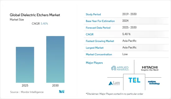
유전체 에칭 세계 시장은 예측 기간 동안 5.4%의 CAGR을 기록할 것으로 예상됩니다.
주요 하이라이트
- 뉴로모픽 칩 수요 증가로 에처 시장 견인 인공지능, 데이터 처리 및 분석에 대한 수요 증가는 전 세계 뉴로모픽 칩의 혁신과 채택에 영향을 미치는 주요 요인입니다. 에칭 기술은 웨이퍼의 코팅과 재료를 선택적으로 제거하여 칩의 특징을 만드는 데 도움이 됩니다. 이러한 절차는 제거하기 어려운 재료의 조합으로 점점 더 작고 복잡한 특징을 만들어야 합니다.
- 유전체 에칭 세계 시장의 최신 동향은 3D IC의 출현입니다. 에너지 소비가 적은 고속 컴퓨팅 장치에 대한 수요가 증가하면서 3D 칩 적층에 대한 수요가 크게 증가하고 있습니다. 항공우주, 자동차, 의료 등의 분야에서 전자 장치의 소형화 요구가 증가함에 따라 0-10nm, 심지어 원자 단위의 정밀도로 구조를 변경할 수 있는 유전체 에칭에 대한 수요가 증가하고 있습니다.
- 에칭 공정은 또한 칩 패키징 및 미세 전기 기계 시스템 통합(MEMS)을 가능하게 하는 스루 실리콘 비아(TSV)와 같은 높은 높이와 높은 종횡비 특성을 생성합니다. 예를 들어, 램리서치의 플라즈마 에칭 시스템은 높고 좁은 구조부터 짧고 넓은 구조, 수 옹스트롬 크기까지 정밀한 구조물을 제작하는 데 필요한 고성능과 높은 생산성을 제공합니다.
- 2021년 5월, 어플라이드 머티어리얼즈는 DRAM의 미세화와 칩 성능, 전력 소비, 면적, 비용 및 시장 출시 기간(PPACt)을 최적화하는 세 가지 새로운 재료 엔지니어링 솔루션을 발표했습니다. 개발한 저유전율 소재인 블랙 다이아몬드를 사용하여 로직 배선의 확장성 문제를 해결하고 있습니다.
- COVID-19의 발생은 2020년 초기에 공급망과 생산에 큰 혼란을 일으켰습니다. 그 영향은 반도체 에칭 장비의 주요 최종사용자인 반도체 제조업체에 더 큰 영향을 미쳤습니다. 인력 부족으로 인해 반도체 공급망의 많은 업체들이 운영을 축소하거나 중단해야 했습니다. 업계는 높은 적자와 수요 증가로 인해 공급망에 큰 격차가 발생했습니다. 바이러스의 초기 확산은 자동차 등 주요 부문의 칩 수요 감소에 대한 우려로 주조 공장의 가동 중단과 가동률 하락으로 이어졌습니다. 생산량 감소는 반도체 파운드리의 당초 예상과 달리 수요가 증가함에 따라 세계 반도체 부족 사태로 이어졌습니다.
유전체 에칭 시장 동향
뉴로모픽 칩에 대한 수요로 유전체 에칭 시장 활성화
- 뉴로모픽 칩은 생물학적 뇌의 처리 능력에서 영감을 얻은 데이터 프로세서로, 수백만 개의 신경 세포의 능력을 가진 고속, 저전력 학습을 실현하는 데이터 프로세서입니다. 이 칩의 크기는 모바일에 적합할 정도로 작고 응용 범위가 넓다.
- 또한, AI 기반 스타트업이 날로 증가하고 있으며, AI로 구현되는 기술은 처리를 위해 뉴로모픽 칩을 필요로 합니다. 따라서 인공지능, 데이터 처리 및 분석에 대한 수요 증가는 전 세계 뉴로모픽 칩의 기술 혁신과 채택에 영향을 미치는 주요 요인으로 유전체 에칭 시장을 주도할 것으로 예상됩니다.
- 인공지능, 데이터 처리 및 분석에 대한 수요 증가는 전 세계적으로 뉴로모픽 칩의 채택을 촉진하는 중요한 요인으로 유전체 에칭에 대한 요구를 창출합니다. 또한, 첨단 지능형 기기를 위한 사물인터넷 애플리케이션의 급속한 기술 업그레이드는 기술적으로 진보된 반도체에 대한 수요를 증가시킬 것으로 예상됩니다. 그 결과 유전체 에칭에 대한 수요가 크게 증가할 것으로 예상됩니다.
- DRAM은 세계 경제의 디지털 전환으로 인해 높은 수요를 보이고 있습니다. 사물인터넷으로 인해 엣지(edge)에 컴퓨터 디바이스가 대량으로 추가되고, 그 결과 처리를 위해 클라우드로 전송되는 데이터가 기하급수적으로 증가하게 됩니다. 업계는 DRAM이 더 빠르게 작동하고, 더 적은 전력을 소비하며, 크기와 비용을 줄일 수 있는 진보를 요구하고 있으며, 이는 시장 성장의 원동력이 되고 있습니다.
- 스마트폰 및 반도체 IC를 필요로 하는 가정용 전자제품 시장의 기타 애플리케이션은 유전체 에칭에 대한 수요를 촉진하고 있습니다. 또한 사물인터넷(IoT) 기기의 수가 증가함에 따라 반도체 업계는 보다 혁신적인 제품을 생산하기 위해 이 기술에 투자하는 것을 목표로 하고 있습니다.
아시아태평양이 가장 큰 비중을 차지
- Qualcomm, Broadcom, Nvidia, MediaTek, Apple, AMD 등 전 세계 집적 디바이스 제조업체(IDM)는 팹리스 비즈니스 모델을 채택하고 있습니다. 팹리스 비즈니스 모델은 매출 유지에 필요한 높은 생산량을 유지하면서 신기술 연구개발에 이익을 집중 투자할 수 있게 해줍니다.
- TSMC, UMC, DB Hitek, SMIC와 같은 조직은 고객의 요구 사양과 생산량에 따라 칩셋을 생산하기 위해 파운드리를 이용하고 있습니다. 이들 파운드리의 대부분은 중국, 대만, 한국에서 운영되고 있습니다.
- 원자층 에칭(ALE)은 얕은 구조에서 뛰어난 깊이 제어를 제공하는 정교한 에칭 공정입니다. 디바이스의 피처 크기가 작아짐에 따라 성능 향상에 필요한 정밀도를 달성하기 위해 ALE의 필요성이 증가하고 있습니다.
- 최첨단 마이크로일렉트로닉스 소자 제조에는 고충실도 패턴 전사(에칭)가 필요합니다. 피처가 10nm 이하로 축소되고 새로운 디바이스가 초박형 2D 재료를 사용함에 따라 원자 단위의 정밀도가 더욱 중요해집니다. 이에 따라 원자 수준에서 기존(연속) 에칭의 한계를 극복하는 기술인 원자층 에칭(ALE)에 대한 수요가 증가했습니다.
- TSMC는 애플의 A 시리즈 칩을 독점적으로 생산하고 있습니다. 이 칩셋은 A13이라는 7 나노 미터 칩셋을 사용하여 제조됩니다. 또한 아시아태평양에는 자동차 전자 산업이 매우 활발하고 시장 성장 기회가 풍부합니다.
유전체 에칭 산업의 개요
유전체 에칭 세계 시장은 매우 경쟁이 치열합니다. 크고 작은 기업이 존재하기 때문에 시장은 매우 집중되어 있습니다. 주요 기업들은 모두 시장에서 큰 점유율을 차지하고 있으며, 전 세계 소비자 기반을 확대하는 데 주력하고 있습니다. 이 시장의 주요 기업으로는 Applied Materials Inc., Hitachi High-Technologies Corporation, Lam Research Corporation, Tokyo Electron, Mattson Technology, Inc, Advanced Micro-Fabrication Equipment, Inc. Advanced Micro-Fabrication Equipment Inc. 등이 있습니다. 이들 기업은 예측 기간 동안 경쟁력을 확보하기 위해 여러 파트너십을 체결하고 신제품 출시에 투자함으로써 시장 점유율을 확대할 것으로 예상됩니다.
- 2022년 7월 - 도쿄일렉트론과 IBM, 유리 웨이퍼 기반의 필요성을 없애고 공정을 간소화하는 최신 전면 3D 칩 적층에 협력 IBM과 도쿄일렉트론은 3D 칩 제조를 위한 실리콘 캐리어 웨이퍼를 결함 없이 구현할 수 있는 방법을 발견했습니다. 이 공정은 새로운 300mm 모듈을 통해 입증되었으며, 양사는 300mm 수준의 3D 적층 실리콘 칩 웨이퍼는 이번이 처음이라고 밝혔습니다. IBM은 3D 칩 적층 기술에 대한 막대한 투자가 반도체 생산 공정을 간소화하고 세계 칩 부족 문제를 해결할 수 있을 것으로 기대하고 있습니다. 한줄기 빛이 될 것으로 기대하고 있습니다.
- 2022년 6월 - 램리서치, SK 하이닉스와 협력하여 드라이 레지스트 극자외선 기술로 DRAM 생산 비용 효율을 높입니다. 램리서치의 혁신적인 건식 레지스트 제조 기술은 첨단 DRAM 칩을 생산하기 위한 두 가지 핵심 공정 개발 도구로, 2020년 램리서치가 도입한 건식 레지스트 기술은 차세대 반도체 생산에 있어 매우 중요한 기술인 EUV(극자외선) 리소그래피의 수율, 해상도, 생산성 및 생산성을 향상시킵니다. 램리서치의 건식 레지스트 기술은 재료 수준에서 EUV 리소그래피의 가장 큰 도전과제를 해결하고, 첨단 메모리와 로직을 위한 비용 효율적인 스케일링을 가능하게 합니다.
기타 혜택:
- 엑셀 형식의 시장 예측(ME) 시트
- 3개월간의 애널리스트 지원
목차
제1장 소개
- 조사 가정과 시장 정의
- 조사 범위
제2장 조사 방법
제3장 주요 요약
제4장 시장 인사이트
- 시장 개요
- 업계의 매력 - Porter's Five Forces 분석
- 공급 기업의 교섭력
- 소비자의 협상력
- 신규 참여업체의 위협
- 대체품의 위협
- 경쟁 기업 간의 경쟁 강도
- COVID-19의 시장에 대한 영향
제5장 시장 역학
- 시장 성장 촉진요인
- 뉴로모픽칩 세계 수요
- 3D IC의 출현
- 전자 디바이스 소형화
- 시장 과제/억제요인
- 초기 비용 상승
제6장 시장 세분화
- 유형별
- 웨트 에칭
- 드라이 에칭
- 원자 레벨 에칭(ALE)
- 지역별
- 북미
- 유럽
- 아시아태평양
- 기타 지역
제7장 경쟁 구도
- 기업 개요
- Applied Materials, Inc.
- Hitachi High-Technologies Corporation
- Lam Research Corporation
- Tokyo Electron Limited
- Mattson Technology
- Advanced Micro-Fabrication Equipment Inc.
- Jusung Engineering
- Oxford Instruments
- SEMES Co. Ltd.
- ULVAC, Inc.
제8장 투자 분석
제9장 시장 전망
ksm 25.01.23The Global Dielectric Etchers Market is expected to register a CAGR of 5.4% during the forecast period.

Key Highlights
- An increase in demand for neuromorphic chips will drive the market for etchers. The rising demand for artificial intelligence, data processing & analytics is a major factor influencing the innovation & adoption of neuromorphic chips across the globe. Etch techniques aid in creating chip features by eliminating coatings and materials put on the wafer selectively. These procedures entail producing increasingly small and intricate features with difficult-to-remove material combinations.
- The latest trend in the global dielectric etchers market is the emergence of 3D ICs. With the increasing demand for faster computing devices that consume less amount of energy will significantly drive the demand for 3D chip stacking. The growing need for miniaturizing electronic devices in fields such as Aerospace, Automotive & Medical sectors will drive the demand for dielectric etchers, which are capable of altering structures to a precision of 0 - 10 nm & even at an atomic level.
- Etch methods also produce tall, high-aspect-ratio features, like through-silicon vias (TSVs), which allow chip packaging and micro-electromechanical system integration (MEMS). For instance, Lam Research plasma etch systems provide high-performance and high-productivity capabilities required to build precise structures, ranging from tall and narrow, short and wide, to a few angstroms in size.
- In May 2021, Applied Materials, Inc. announced three new materials engineering solutions that enable its memory customers three new options to scale DRAM and optimize chip performance, power, area, cost, and time to market (PPACt). DRAM manufacturers use black diamond, a low-k dielectric material developed by Applied Materials, to solve logic interconnect scalability problems.
- The outbreak of COVID-19 significantly disrupted the supply chain and production during the initial phase of 2020. The impact was more severe for semiconductor manufacturers, the major end users for semiconductor etch equipment. Due to labor shortages, many players in the semiconductor supply chain had to reduce or even suspend their operations. The industry was riddled with a high deficit and increasing demand, which led to a significant supply chain gap. The initial spread of the virus led to the shutting down or reduction of foundry capacity utilization, fearing the decreasing demand for chips across major sectors, like the automotive. Diminished output led to a global shortage of semiconductors as demand increased, despite the initial estimates by semiconductor foundries.
Dielectric Etchers Market Trends
Demand for Neuromorphic Chip to Boost Dielectric Etchers Market
- A neuromorphic chip is a data processor inspired by biological brain processing ability to achieve high-speed & low power learning and constructed with capabilities of millions of neurons. The size of these chips is small enough to go mobile, and applications are broad.
- Besides, AI-based startups are increasing day by day. The technologies enabled by AI require neuromorphic chips for processing. Therefore, the rising demand for artificial intelligence, data processing & analytics is a major factor influencing the innovation & adoption of neuromorphic chips across the globe, which in turn is expected to drive the market for dielectric etchers.
- The rising demand for artificial intelligence, data processing, and analytics is a significant factor that drives the adoption of neuromorphic chips worldwide, thereby creating the need for dielectric etchers. Moreover, rapid technological upgradation of Internet of Things applications for advanced intelligent devices is also anticipated to boost the demand for technologically advanced semiconductors. This, in turn, is predicted to create significant demand for dielectric etching in the market.
- DRAM is in high demand due to the global economy's digital transition. The Internet of Things creates significant additional computer devices at the edge, resulting in an exponential rise in data that is transported to the cloud for processing. The industry needs advancements that would allow DRAM to scale down in size and cost while running at greater speeds and consuming less power, which drives the market growth.
- Smartphones and other applications in the consumer electronics market that require semiconductor ICs drive the demand for dielectric etcher. Furthermore, as the number of Internet of Things (IoT) devices grows, the semiconductor industry aims to invest in this technology to produce more innovative products.
Asia Pacific Region to Hold a Significant Share
- Integrated Device Manufacturers (IDM) such as Qualcomm, Broadcom Ltd., Nvidia, MediaTek, Apple, AMD, etc. across the globe are adopting fabless business model, where the organization will design the chipset layout and outsource the manufacturing to chipset manufacturers such as TSMC, UMC & SMIC. The fabless business model helps organizations to concentrate their efforts on investing profits in research and development of new technologies while maintaining the high production volumes needed to maintain sales.
- Organizations such as TSMC, UMC, DB Hitek, SMIC, etc. utilize their foundries to produce the chipset according to the specifications and volumes requirement of the customers. A major share of these foundries operates from China, Taiwan & South Korea.
- Atomic layer etching (ALE) is a sophisticated etching process that provides superior depth control on shallow structures. As device feature size shrinks, ALE becomes increasingly necessary to attain the accuracy required for enhanced performance.
- The production of advanced microelectronic devices requires high-fidelity pattern transfer (etching). As features drop to sub-10nm sizes and new devices use ultra-thin 2D materials, atomic-scale accuracy becomes more important. This raised the demand for atomic layer etching (ALE), a technique that overcomes the limits of traditional (continuous) etching at the atomic level.
- TSMC has been Apple's exclusive manufacturer of Apple's A-series chips. This chipset will be fabricated using a 7-nanometer chipset called A13. Besides, with automotive electronics industry flourishing exceedingly in the region, Asia-Pacific is providing a plethora of opportunities for market growth.
Dielectric Etchers Industry Overview
The Gloabl Dielectric Etchers Market is very competitive in nature. The market is highly concentrated due to the presence of various small and large players. All the major players account for a large share of the market and are focusing on expanding their consumer base across the world. Some of the significant players in the market are Applied Materials Inc., Hitachi High-Technologies Corporation, Lam Research Corporation, Tokyo Electron, Mattson Technology, Inc., Advanced Micro-Fabrication Equipment Inc., and many more. The companies are increasing the market share by forming multiple partnerships and investing in introducing new products to earn a competitive edge during the forecast period.
- July 2022 - Tokyo Electron and IBM collaborated for the latest front 3D chip stacking that removes the need for a glass wafer base, streamlining the process. IBM and Tokyo Electron, however, have found a way to enable silicon carrier wafers for 3D chipmaking without the drawbacks. This process was demonstrated using a new 300mm module, which the companies say is the first 3D stacked silicon chip wafer at the 300mm level. IBM hopes that the considerable investments in 3D chip stacking technology can help streamline the production process of semiconductors and offer a silver lining to the global chip shortage.
- June 2022 - Lam Research collaborated with SK Hynix to enhance DRAM production cost efficiency with dry resist Extreme Ultraviolet technology. Lam's innovative dry resist fabrication technology is a development tool for two key process steps for producing advanced DRAM chips. This technology introduced by LAM in 2020, dry resist, extends the yield, resolution, productivity, and of EUV (Extreme Ultraviolet) lithography, a pivotal technology in producing next-generation semiconductors. At the material level, Lam's dry resist technology addresses EUV lithography's biggest challenges, enabling cost-effective scaling for advanced memory and logic.
Additional Benefits:
- The market estimate (ME) sheet in Excel format
- 3 months of analyst support
TABLE OF CONTENTS
1 INTRODUCTION
- 1.1 Study Assumptions and Market Definition
- 1.2 Scope of the Study
2 RESEARCH METHODOLOGY
3 EXECUTIVE SUMMARY
4 MARKET INSIGHTS
- 4.1 Market Overview
- 4.2 Industry Attractiveness - Porter's Five Forces Analysis
- 4.2.1 Bargaining Power of Suppliers
- 4.2.2 Bargaining Power of Consumers
- 4.2.3 Threat of New Entrants
- 4.2.4 Threat of Substitutes
- 4.2.5 Intensity of Competitive Rivalry
- 4.3 Impact of COVID-19 on the Market
5 MARKET DYNAMICS
- 5.1 Market Drivers
- 5.1.1 Global Demand of Neuromorphic Chip
- 5.1.2 Emergence of 3D ICs
- 5.1.3 Miniaturizing Electronic Devices
- 5.2 Market Challenge/Restraint
- 5.2.1 Higher Initial Costs
6 MARKET SEGMENTATION
- 6.1 By Type
- 6.1.1 Wet Etching
- 6.1.2 Dry Etching
- 6.1.3 Atomic Level Etching (ALE)
- 6.2 By Geography
- 6.2.1 North America
- 6.2.2 Europe
- 6.2.3 Asia Pacific
- 6.2.4 Rest of the World
7 COMPETITIVE LANDSCAPE
- 7.1 Company Profiles
- 7.1.1 Applied Materials, Inc.
- 7.1.2 Hitachi High-Technologies Corporation
- 7.1.3 Lam Research Corporation
- 7.1.4 Tokyo Electron Limited
- 7.1.5 Mattson Technology
- 7.1.6 Advanced Micro-Fabrication Equipment Inc.
- 7.1.7 Jusung Engineering
- 7.1.8 Oxford Instruments
- 7.1.9 SEMES Co. Ltd.
- 7.1.10 ULVAC, Inc.