|
시장보고서
상품코드
1690752
반도체 리소그래피 장비 : 시장 점유율 분석, 산업 동향 및 통계, 성장 예측(2025-2030년)Semiconductor Lithography Equipment - Market Share Analysis, Industry Trends & Statistics, Growth Forecasts (2025 - 2030) |
||||||
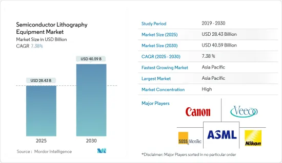
반도체 리소그래피 장비 시장 규모는 2025년 284억 3,000만 달러로 평가되었고, 2030년 405억 9,000만 달러에 이를 것으로 예측되며, 예측 기간(2025-2030년)의 CAGR은 7.38%를 나타낼 전망입니다.

주요 하이라이트
- 반도체 리소그래피 장비 시장은 가전, 자동차 등 거의 모든 분야에서 널리 사용되는 반도체 디바이스의 제조가 증가함에 따라 성장할 것으로 예상됩니다. 스마트 기기 채택이 증가하고 있으며, 5G 연결과 채택이 전 세계로 확산됨에 따라 성장세를 보일 것으로 예상됩니다.
- 반도체 FAB(제조) 비용의 50% 이상이 장비와 도구에 의해 발생합니다. 반도체 제조 공정을 발전시키는 장비 중 하나는 리소그래피입니다. 반도체 제조에는 리소그래피 장비가 주도하는 몇 가지 측면이 있습니다.
- 반도체 제품의 복잡성이 증가함에 따라 결함의 유형도 복잡해지고 있습니다. 하지만 리소그래피 장비는 복잡한 공정을 처리해야 합니다.
- 또한 최근 제조업은 5G의 도래와 IoT 연결 장치의 등장으로 무선 제어와 같은 다양한 인더스트리 4.0 용도에 필요한 연결이 용이해질 것으로 예상되는 가운데 상당한 속도로 성장하고 있습니다.
- 2022년 3월, Nikon Corporation은 하이엔드 모니터, 대형 TV, 스마트 기기 등 고부가가치 프리미엄 디스플레이를 위한 다양한 고화질 패널 생산을 지원하기 위해 새로운 8세대 플레이트 FPD 리소그래피 시스템을 출시한다고 발표했습니다.
- 반도체 산업은 제조, 검사 등 500개 이상의 공정 단계와 다양한 제품이 존재할 뿐만 아니라 변동성이 큰 전자 시장과 예측하기 어려운 수요 등 열악한 환경으로 인해 가장 복잡한 산업 중 하나로 꼽힙니다. 따라서 제조 공정의 복잡성에 따라 반도체 웨이퍼의 전체 제조 및 검사에만 약 1,400개의 공정 단계가 존재합니다
반도체 리소그래피 장비 시장 동향
주요 시장 점유율을 차지하는 심자외선 리소그래피(DUV)
- 심자외선 리소그래피(DUV)는 4X 또는 5X 광학 시스템을 통해 마스크의 패턴을 웨이퍼 표면에 투사하는 광학 투영 리소그래피 기술입니다. 이 유형의 리소그래피에 사용되는 파장은 248nm 또는 193nm입니다. 이 리소그래피는 DUV 툴의 일반적인 웨이퍼 레벨 노출 필드 크기인 22mm x 22mm보다 크지 않은 이산 부품의 대면적 마스터에 이상적인 고속 리소그래피 기술입니다.
- DUV 리소그래피 방식은 차세대 리소그래피 기술을 선도하는 기술 중 하나입니다. 이 기술은 비용 효율적이며 해상도가 향상되었습니다.
- DUV 리소그래피를 사용하면 전력 요구량이 낮은 경량 전자 칩을 쉽게 만들 수 있습니다. 이 플랫폼은 향상된 전력 분해능과 비용 효율성이 특징입니다. 이러한 구조가 모여 칩으로 알려진 IC를 형성합니다. 반도체 업계가 더 효율적인 마이크로칩을 찾는다는 것은 칩 제조업체가 칩에 더 많은 구조를 연구하여 칩을 더 빠르고 효율적으로 만드는 동시에 생산 비용을 절감해야 한다는 것을 의미합니다. 이는 예측 기간 동안 시장의 성장을 촉진할 것으로 예상됩니다.
- ASML에 따르면 EUV로의 전환은 DUV에 대한 수요만 증가시킬 수 있습니다
- WSTS에 따르면 2024년 1월 유럽의 반도체 매출은 2023년 1월의 44억 8,000만 달러에서 소폭 감소한 44억 2,000만 달러를 기록했습니다.
- 이러한 개발과 정부의 반도체 생산 증대를 위한 노력은 예측 기간 동안 시장 성장을 주도할 것으로 예상됩니다.
큰 점유율을 차지하는 미국
- 미국은 강력한 반도체 R&D 역량, 반도체 제조 역량 확대를 위한 상당한 투자, 첨단 기술의 빠른 도입을 자랑합니다.
- 또한, 미국은 반도체에 대한 수요 증가를 목격하고 있습니다. 예를 들어, 2021년 9월 세계 반도체 무역 통계(WSTS)에 따르면 2021년 반도체 산업 매출은 5,270억 달러로 크게 증가했으며, 이는 2020년 전체 시장의 강력한 수요 성장으로 인해 2021년 전망치가 2020년보다 상향 조정된 것입니다.
- 게다가 2022년 4월, Semiconductor Equipment and Materials International에 따르면, 북미의 반도체 장비에의 지출은 2020년의 65억 3,000만 달러에 대해, 2021년은 76억 1,000만 달러에 달했습니다.
- 미국 반도체 산업 현황에 따르면 반도체 칩으로 작동하는 커넥티드 디바이스(예: 사물인터넷(IoT))는 2019년에 226억 달러를 기록했으며 2025년에는 750억 달러에 달할 것으로 예상됩니다. 반도체는 또한 3D 프린팅, 머신러닝, 인공지능(AI) 등 의료 서비스를 개선하고, 건축 비용을 절감하며, 식량 공급을 강화하고, 과학의 발전을 가능하게 하는 혁신의 기반이 됩니다.
- 게다가 2022년 9월 바이덴 정권은 중국에 대한 미국의 경쟁력을 강화하기 위한 행정부의 노력의 일환으로 2022년 8월 국내 첨단 기술 제조 부양을 위해 2,800억 달러 규모의 반도체 법안에 서명했습니다. 이 지역의 반도체 부문에 대한 이러한 강력한 투자는 연구 대상 시장의 성장에 유리한 기회를 제공할 것입니다.
반도체 리소그래피 장비 산업 개요
반도체 리소그래피 장비 시장은 ASML, Veeco, Nikon과 같은 소수의 기업이 대부분의 시장 점유율을 차지하고 있어 집중화되어 있습니다. 반도체 제조를 위한 핵심 장비는 기본적으로 미국과 일본 기업이 독점하고 있습니다. 통합과 기술 발전, 지정학적 시나리오가 증가함에 따라 연구 대상 시장은 변동을 목격하고 있습니다. 또한 수직 통합이 증가함에 따라 연구 대상 시장의 경쟁 강도는 수익에서 비롯되는 투자 능력을 고려할 때 계속 증가 할 것으로 예상됩니다.
- 2022년 9월 : Canon Inc.반도체 리소그래피 시스템용 솔루션 플랫폼 'Lithography Plus1'를 출시했습니다. 반도체 리소그래피 시스템 지원 분야에서 50년 이상 쌓아온 Canon의 경험과 회사의 방대한 데이터를 시스템에 통합하여 지원 효율성을 극대화하고 최적화된 시스템 프로세스를 제안 및 구현합니다.
- 2022년 6월 : 삼성과 ASML은 내년에 출시될 High-NA EUV 노광 장비 개발을 위해 협력하기로 합의했습니다. 차세대 고난도 EUV 노광 장비는 기존 노광 장비에 비해 더 미세한 회로를 새길 수 있습니다.
기타 혜택
- 엑셀 형식 시장 예측(ME) 시트
- 3개월간의 애널리스트 지원
목차
제1장 서론
- 조사의 전제조건과 시장 정의
- 조사 범위
제2장 조사 방법
제3장 주요 요약
제4장 시장 인사이트
- 시장 개요
- 산업의 매력 - Porter's Five Forces 분석
- 공급기업의 협상력
- 구매자의 협상력
- 신규 진입업자의 위협
- 대체품의 위협
- 경쟁 기업간 경쟁 관계
- 반도체 리소그래피 장비의 기술 로드맵
- 거시 경제 동향이 시장에 미치는 영향
제5장 시장 역학
- 시장 성장 촉진요인
- 전기자동차 및 첨단 모바일 기기의 소형화 및 추가 기능에 대한 수요 증가
- 새로운 리소그래피 도구를 제공하는 전문 장비 공급 업체의 혁신 성장
- 시장 성장 억제요인
- 제조 공정에서 패턴의 복잡성과 관련된 과제
제6장 시장 세분화
- 유형
- 심자외선 리소그래피(DUV)
- 극자외선 리소그래피(EUV)
- 신청
- 첨단 포장
- MEMS 디바이스
- LED 디바이스
- 지역
- 북미
- 유럽
- 아시아
- 호주 및 뉴질랜드
- 라틴아메리카
- 중동 및 아프리카
제7장 경쟁 구도
- 기업 프로파일
- Canon Inc.
- Nikon Corporation
- ASML Holding NV
- Veeco Instruments Inc.
- SUSS MicroTec SE
- Shanghai Micro Electronics Equipment(Group) Co. Ltd
- EV 그룹(EVG)
- JEOL Ltd
- Onto Innovation(Rudolph Technologies Inc.)
- Neutronix Quintel Inc.(NXQ)
- 벤더의 시장 점유율 분석
제8장 투자 분석
제9장 시장의 미래
HBR 25.05.09The Semiconductor Lithography Equipment Market size is estimated at USD 28.43 billion in 2025, and is expected to reach USD 40.59 billion by 2030, at a CAGR of 7.38% during the forecast period (2025-2030).
Key Highlights
- The semiconductor lithography equipment market is expected to grow with the growing manufacturing of semiconductor devices that are widely used in nearly all sectors including consumer electronics, automotive, and many others. Smart device adoption is increasing and is expected to grow as 5G connections and adoption spread over the globe. As per GSMA, 5G mobile broadband connections are expected to reach 1,100 million by 2025, with the 5G rollout expected to cover 34 percent of the world's population by 2025.
- More than 50 percent of the semiconductor FAB (fabrication) cost is due to equipment and tools. One piece of equipment that drives the semiconductor fabrication process forward is lithography. There are several aspects of semiconductor fabrication that has driven by lithography equipment. Yield and defect are two such examples from the technical point of view. It is the primary reason why semiconductor fabrication focuses a lot on which type of lithography technology to deploy.
- With the rising complexity in semiconductor products, the types of defects are also getting complex. However, lithography equipment is supposed to handle the complex process. With semiconductor manufacturers focusing on next-gen advanced technology nodes, the importance of error-free lithography equipment is significantly increasing further.
- Moreover, manufacturing businesses are are lately growing at a signficant rate with the advent of 5G and emergence of IoT connected devices, which is anticipated to facilitate the connection required for various Industry 4.0 applications, such as wireless control. This is especially essential for mobile tools, machines, and robots that can aid market growth during the forecast period.
- Several industry players are focusing on offering new lithography systems to serve a wide range of applications. For instance, in March 2022, Nikon Corporation announced to launch new Gen 8 plate FPD lithography system to support the production of various high-definition panels for value-added premium displays, such as high-end monitors, large TVs, and smart devices.
- The semiconductor industry is considered as one of the most complex industries, not only owing to the presence of more than 500 processing steps involved in the manufacturing and inspection and various products but also due to the harsh environment it goes through, e.g., the volatile electronic market and the unpredictable demand. Therefore, depending on the intricacy of the manufacturing process, there are about 1,400 process steps in the complete manufacturing and inspection of semiconductor wafers alone. Such a complex process poses a notable hurdle to the market's growth.
Semiconductor Lithography Equipment Market Trends
Deep Ultraviolet Lithography (DUV) to Hold Major Market Share
- Deep UV lithography (DUV) is an optical projection lithography technique where the pattern on the mask is projected to the wafer surface through a 4X or 5X optical system. The wavelengths used for this type of lithography are 248 nm or 193 nm. This lithography is a high-speed lithographic technology ideal for large-area masters of discrete components that are not bigger than 22 mm x 22 mm, the typical wafer-level exposure field size of a DUV tool.
- The DUV lithography type is one of the leading lithography technologies of the next generation. The technology is cost-effective and has increased resolving power. The adoption of DUV lithography is driven primarily by the miniaturization trend. Lithography is used for printing complex patterns that characterize integrated circuits (ICs) on semiconductor wafers.
- Using DUV lithography, lightweight electronic chips with lower power demands are easy to achieve. The platform features enhanced power resolution and is cost-effective. These structures together form an IC, which is known as a chip. The semiconductor industry's search for even more efficient microchips means chipmakers have to study more structures onto a chip, making the chip faster and more efficient while also reducing production costs. This is expected to boost the market's growth over the forecast period.
- According to ASML, a transition to EUV may only boost demand for DUV. Chip manufacturers deploy EUV in the early stages of chip fabrication to apply the minor structures: transistors, smallest vias (the contacts that connect the source, gate, and drain to the complex interconnect layers), and possibly the connecting layer.
- According to WSTS, Semiconductor sales in Europe reached 4.42 billion USD in January 2024, a slight decrease from the 4.48 billion USD reported in January 2023. Global semiconductor sales hit 47.63 billion U.S. dollars in January 2024 when considering the overall market.
- Such developments by the major vendors, along with the initiatives taken by the government to boost their semiconductor production, are expected to drive market growth over the forecast period.
United States to Witness Significant Share
- The United States boasts robust semiconductor R&D capabilities, significant investments catering to the expansion of semiconductor manufacturing capabilities, and rapid adoption of advanced technologies.
- Further, the United States is witnessing an increasing demand for semiconductors. For instance, in September 2021, according to the world semiconductor trade statistics (WSTS), semiconductor industry sales increased significantly to USD 527 billion in 2021, an upward revision from the 2020 forecast for 2021 due mainly to the strong demand growth in the overall market 2020. In 2022, WSTS forecasted global sales totaled to USD 573 billion.
- Additionally, in April 2022, according to Semiconductor Equipment and Materials International, North America's spending on semiconductor equipment reached USD 7.61 billion in 2021 compared to 2020, which was USD 6.53 billion.
- Also, the semiconductor industry association stated that the US semiconductor industry is a leader in chip design. The United States fabless firms account for roughly 60 percent of all global fabless firm sales, and some of the largest IDMs, which make their arrangement, are also US firms.
- According to the state of the US semiconductors industry, the connected devices that run on semiconductor chips (i.e., the Internet of Things (IoT)) registered USD 22.6 billion in 2019 and are expected to reach USD 75 billion by 2025. Semiconductors are also fundamental to innovations, such as 3D printing, machine learning, and artificial intelligence (AI) that enhance healthcare, reduce building costs, strengthen food supply, and enable advancements in science. The region's robust semiconductor demand is likely to boost the adoption of semiconductor lithography equipment during the forecast period.
- Additionally, in September 2022, the Biden administration announced that it would invest USD 50 billion in building up the domestic semiconductor industry to counter dependency on China, as the US produces zero and consumes 25 percent of the world's leading-edge chips vital for its national security. President Joe Biden signed a USD 280 billion CHIPS bill in August 2022 to boost domestic high-tech manufacturing, part of his administration's push to boost US competitiveness over China. Such robust investments in the semiconductor sector in the region would offer lucrative opportunities for the growth of the studied market.
Semiconductor Lithography Equipment Industry Overview
The market is concentrated due to a few vendors such as ASML, Veeco, and Nikon occupying the majority market share. The key equipment for semiconductor manufacturing is basically monopolized by American and Japanese companies. With growing consolidation and technological advancement, and geopolitical scenarios, the studied market is witnessing fluctuation. In addition, with increasing vertical integration, the intensity of competition in the studied market is expected to continue to rise, considering their ability to invest, which results from their revenues.
- September 2022 - Canon Inc. launched the "Lithography Plus1" solution platform for semiconductor lithography systems. Canon's more than 50 years of experience in semiconductor lithography system support and the company's vast wealth of data are incorporated into the system to maximize support efficiency and propose and implement optimized system processes.
- June 2022 - Samsung and ASML have agreed to collaborate on developing High-NA (high numerical aperture) EUV Lithography equipment, which will be available next year. Compared to older EUV Lithography equipment, the next-generation High-NA EUV Lithography equipment can engrave finer circuits.
Additional Benefits:
- The market estimate (ME) sheet in Excel format
- 3 months of analyst support
TABLE OF CONTENTS
1 INTRODUCTION
- 1.1 Study Assumptions and Market Definition
- 1.2 Scope of the Study
2 RESEARCH METHODOLOGY
3 EXECUTIVE SUMMARY
4 MARKET INSIGHTS
- 4.1 Market Overview
- 4.2 Industry Attractiveness - Porter's Five Forces Analysis
- 4.2.1 Bargaining Power of Suppliers
- 4.2.2 Bargaining Power of Buyers
- 4.2.3 Threat of New Entrants
- 4.2.4 Threat of Substitute Products
- 4.2.5 Intensity of Competitive Rivalry
- 4.3 Semiconductor Lithography Equipment Technology Roadmap
- 4.4 The impact of macroeconomic trends on the Market
5 MARKET DYNAMICS
- 5.1 Market Drivers
- 5.1.1 Increasing Demand for Miniaturization and Extra Functionality by Electric Vehicles and Advanced Mobile Devices
- 5.1.2 Growing Innovation by Specialist Equipment Vendors offering Brand New Lithography Tools
- 5.2 Market Restraints
- 5.2.1 Challenges Regarding Complexity of Pattern in Manufacturing Process
6 MARKET SEGMENTATION
- 6.1 Type
- 6.1.1 Deep Ultraviolet Lithography (DUV)
- 6.1.2 Extreme Ultraviolet Lithography (EUV)
- 6.2 Application
- 6.2.1 Advanced Packaging
- 6.2.2 MEMS Devices
- 6.2.3 LED Devices
- 6.3 Geography
- 6.3.1 North America
- 6.3.2 Europe
- 6.3.3 Asia
- 6.3.4 Australia and New Zealand
- 6.3.5 Latin America
- 6.3.6 Middle East and Africa
7 COMPETITIVE LANDSCAPE
- 7.1 Company Profiles
- 7.1.1 Canon Inc.
- 7.1.2 Nikon Corporation
- 7.1.3 ASML Holding NV
- 7.1.4 Veeco Instruments Inc.
- 7.1.5 SUSS MicroTec SE
- 7.1.6 Shanghai Micro Electronics Equipment (Group) Co. Ltd
- 7.1.7 EV Group (EVG)
- 7.1.8 JEOL Ltd
- 7.1.9 Onto Innovation (Rudolph Technologies Inc.)
- 7.1.10 Neutronix Quintel Inc. (NXQ)
- 7.2 Vendor Market Share Analysis