|
시장보고서
상품코드
1907281
현미경 기기 시장 : 점유율 분석, 업계 동향, 통계, 성장 예측(2026-2031년)Microscopy Device - Market Share Analysis, Industry Trends & Statistics, Growth Forecasts (2026 - 2031) |
||||||
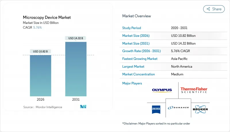
현미경 기기 시장은 2025년 102억 3,000만 달러로 평가되었고, 2026년에는 108억 2,000만 달러, 2026년부터 2031년에 걸쳐 CAGR 5.76%로 성장하고 2031년까지 143억 2,000만 달러에 달할 것으로 예측합니다.

정부에 의한 나노테크놀로지에의 자금 제공, 반도체의 미세화 목표, AI를 활용한 진단 워크플로우가 함께 수요를 재구축해, 현미경을 단순한 화상 취득 툴로부터 예측 분석 엔진으로 진화시키고 있습니다. 게르마늄 공급 제약과 숙련 노동자 부족이 사용자를 자동화로 이끄는 중, 저온 전자 현미경, 양자 센싱, 데스크톱형 초해상 플랫폼이 주목을 받고 있습니다. 주요 벤더는 차세대 기기에 인공지능, 로보틱스, 클라우드 분석을 통합하여 대응하고 있습니다. 성숙한 디지털 병리학, 5나노미터 미만의 칩 제조, 양자재료 연구가 폭넓은 기회 기반을 지원하고, 현미경 기기 시장은 2030년까지 연률 5%대 전반의 성장을 유지할 것으로 전망됩니다.
세계 현미경 기기 시장 동향과 인사이트
현미경 기술의 진보
뮌헨 공과 대학의 양자 감지 현미경은 핵 스핀 신호를 광학 데이터로 변환하여 10나노미터 규모의 세포 세부사항을 포착하여 광 손상을 제거하고 새로운 해상도 기준을 확립했습니다. 절강대학의 구조화 조명중 적외광열현미경은 60나노미터의 화학 이미징을 실현해, 기존 성능을 배가시키는 것과 동시에, 고분자 과학에 불가결한 분자 특이성을 부가하고 있습니다. 얽힌 광자를 이용한 적응 광학 기술은 조직의 왜곡을 추가로 제거하고 기존의 가이드 스타 방법으로 달성 할 수 없었던 선명한 생체 내 이미지를 생성합니다. 이러한 진보가 결합되어 현미경 기기 시장 전체에서 프리미엄 수요를 촉진하고 공급업체의 기능 통합을 촉진하며 사용자의 발견 주기를 단축하고 있습니다.
확대하는 나노기술 및 생명과학 연구개발 자금
미국 국가 나노테크놀로지 이니셔티브는 2025년도에 과거 최고의 22억 달러의 예산을 확보하고, 합성과 실시간 현미경을 조합한 재료 혁신 플랫폼에 자금을 투입하고 있습니다. NSF(미국 과학재단)는 국가 나노기술 협력 인프라에 8,400만 달러를 추가하여 16개 거점에서 선진적 특성 평가 장치의 공유 액세스를 확대했습니다. 미국 국립위생연구소(NIH)의 하이엔드 기기 프로그램은 현미경 시스템에 최대 200만 달러의 보조금을 교부하여 면역요법 및 진단 영상 분야의 기기 풀을 확충하고 있습니다. 민간 기업은 일반적으로 이러한 보조금과 병행하여 공동 투자를 수행하기 때문에 현미경 기기 시장에 미치는 영향이 확대되고 미래의 돌파구 종이 뿌려지고 있습니다.
고액의 자본 비용과 운영 비용
최첨단 세슘 보정형 STEM 장치는 500만 달러에 이르고, 연간 유지보수 비용은 구매 가격의 최대 30%를 소비합니다. 진동 격리, 온도 안정성 및 전자기 차폐를 위한 추가 인프라로 많은 제안이 수백만 달러 규모의 프로젝트가 됩니다. 소규모 대학과 병원은 도입을 망설이고 현미경 기기 시장 내에 2층 고객 기반을 형성하고 있습니다. 2026년에는 ISO 13485를 준수하는 새로운 FDA 규칙이 시행되어 보다 광범위한 품질 문서화가 요구되므로 장비 제조업체의 컴플라이언스 비용이 증가합니다.
부문 분석
전자현미경은 2031년까지 연평균 복합 성장률(CAGR)6.56%로 성장할 전망입니다. 한편, 광학 현미경은 2025년 매출액의 41.78%를 차지했고 생명과학 및 재료연구소에서 일상적인 워크플로우를 계속 지원하고 있습니다. 수차 보정 투과형 전자 현미경은 현재 서브 옹스트롬 수준의 선명도를 달성하고 있으며 반도체 제조 공장 및 제약 연구자에게 필수적인 기술로 자리매김하고 있습니다. 극저온 전자 현미경은 프리미엄 분야를 차지하고 있으며, 단백질 결정화를 회피하고 수용체 부위를 가시화함으로써 항바이러스 및 종양학 프로그램을 가속시킵니다. 히타치 제작소의 SU3900SE는 300mm 웨이퍼와 5kg 샘플에 대응해, 연구 환경에 반도체 그레이드의 스루풋을 가져옵니다.
수요 동향은 대체가 아니라 융합을 강조하고 있습니다. 초해상 광학 시스템은 머신러닝과 연계하여 해상도 갭을 해소하고, 주사형 프로브 현미경은 양자 센서를 활용하여 비접촉 원자 매핑을 실현. 통합 AI 파이프라인은 분석 시간을 대폭 단축하고 진입 장벽을 낮추고 현미경 기기 시장을 꾸준한 기능 확장 궤도에 탑재하고 있습니다.
지역별 분석
북미는 2025년에 39.25%의 수익 점유율을 차지했고 22억 달러 규모의 국가 나노테크놀로지 이니셔티브에 의한 지원과 NIH의 고성능 기기 조성이 견인했습니다. 이 지역에서는 학계와 산업계가 연계한 양자전자현미경 컨소시엄이 활동하고 있어 현미경 기기 시장에서의 주도적 지위를 확고한 것으로 하고 있습니다. 그러나 중국에 의한 게르마늄 및 갈륨의 수출 규제로 렌즈용 게르마늄의 가격은 75% 상승했고, 리드 타임은 40주로 연장되어 공급망의 취약성이 드러났습니다.
아시아태평양은 2031년까지 연평균 복합 성장률(CAGR) 6.74%로 가장 높은 성장을 보여줄 전망입니다. 일본의 반도체 제조장치 매출액 3배화 목표, 중국의 광학기기 국산화 추진, 한국의 파운드리 확장이 함께 설비 투자를 견인하고 있습니다. MA-tek사는 Rapidus사용 500만 달러 상당의 Cs 보정형 TEM 수주에 의해 2025년까지 일본에서의 매출액이 두배로 될 것으로 예측했습니다. 지역 공급망은 정밀 광학 기기를 대량 공급할 수 있지만, 지정학적 마찰에 의한 라이선싱 불확실성에 대해 기업은 합작 사업이나 기술 공유에 의한 안전책으로 대응하고 있습니다.
유럽은 의약품 연구, 정밀 공학의 전통, 이미징 기술 혁신을 키우는 EMBL(유럽 분자 생물학 연구소)과의 연계에 의해 균형 잡힌 성장을 견인합니다. ISO 13485 표준의 조화로 인해 경계 장비 승인이 간소화되고 독일 연방주 프로그램이 연구소의 설비 갱신을 조성하고 있습니다. 숙련 노동력 부족과 아시아 경쟁 격화가 성장 가속을 억제하는 한편, 공간 생물학과 양자 재료 분야의 고부가가치 틈새 시장이 현미경 기기 시장의 기세를 유지하고 있습니다.
기타 혜택 :
- 엑셀 형식 시장 예측(ME) 시트
- 애널리스트에 의한 3개월간의 지원
자주 묻는 질문
목차
제1장 서론
- 조사의 전제조건과 시장의 정의
- 조사 범위
제2장 조사 방법
제3장 주요 요약
제4장 시장 상황
- 시장 개요
- 시장 성장 촉진요인
- 현미경 기술의 기술적 진보
- 나노기술 및 생명과학 분야에서 R&D 자금 증가
- 반도체 기기의 소형화
- AI를 활용한 자동화 디지털 병리 워크플로우
- 구조 기반 신약 개발 극저온 전자 현미경법의 급속한 보급
- 현장 품질 관리 데스크톱 초해상 시스템 도입 증가
- 시장 성장 억제요인
- 높은 자본 비용 및 운영 비용
- 숙련된 현미경 전문가(Microscopist) 부족
- 산학 기술 이전의 지적 재산 소송 위험
- 정밀 광학 기기 공급망 병목 현상
- 가치/공급망 분석
- 규제 상황
- 기술의 전망
- Porter's Five Forces 분석
- 신규 참가업체의 위협
- 구매자의 협상력
- 공급기업의 협상력
- 대체품의 위협
- 경쟁 기업간 경쟁 관계
제5장 시장 규모와 성장 예측
- 현미경유형별
- 전자현미경
- 투과 전자현미경(TEM)
- 주사 전자현미경(SEM)
- 극저온 전자현미경(Cryo-EM)
- 광학현미경
- 명시야 및 위상차
- 형광 및 공초점
- 기타
- 주사 프로브 현미경
- 기타 기술
- 전자현미경
- 용도별
- 나노기술 조사
- 생명과학
- 반도체 및 전자 기기
- 재료과학 및 금속학
- 기타
- 최종 사용자별
- 병원, 진료소 및 진단실험실
- 학술 및 연구기관
- 제약 및 바이오테크놀러지 기업
- 반도체 및 전자 기기 제조업체
- 기타
- 지역별
- 북미
- 미국
- 캐나다
- 멕시코
- 유럽
- 독일
- 영국
- 프랑스
- 이탈리아
- 스페인
- 기타 유럽
- 아시아태평양
- 중국
- 일본
- 인도
- 호주
- 한국
- 기타 아시아태평양
- 중동 및 아프리카
- GCC
- 남아프리카
- 기타 중동 및 아프리카
- 남미
- 브라질
- 아르헨티나
- 기타 남미
- 북미
제6장 경쟁 구도
- 시장 집중도
- 시장 점유율 분석
- 기업 프로파일
- Thermo Fisher Scientific(FEI)
- Carl Zeiss AG
- Danaher Corp.(Leica Microsystems)
- Hitachi High-Tech Corp.
- JEOL Ltd.
- Nikon Corp.
- Olympus Corp.
- Bruker Corp.
- Park Systems Corp.
- Tescan Orsay Holding
- Labomed Inc.
- Andor Technology Ltd.
- Oxford Instruments PLC
- Becton Dickinson & Co.
- Asylum Research
- NT-MDT Spectrum Instruments
- Ametek(Cameca)
- ASML Holding(Nikon Metrology)
- Keyence Corp.
- Cytovale Inc.
제7장 시장 기회와 장래의 전망
SHW 26.01.26The microscopy devices market is expected to grow from USD 10.23 billion in 2025 to USD 10.82 billion in 2026 and is forecast to reach USD 14.32 billion by 2031 at 5.76% CAGR over 2026-2031.
Government nanotechnology funding, semiconductor miniaturization goals and AI-enabled diagnostic workflows jointly re-shape demand , elevating microscopes from image capture tools to predictive analytics engines. Cryo-electron microscopy, quantum sensing and desktop super-resolution platforms gain traction as germanium supply constraints and skilled-labor shortages push users toward automation. Leading vendors respond by embedding artificial intelligence, robotics and cloud analytics into next-generation instruments. Maturing digital pathology, sub-5-nanometer chip production and quantum materials research sustain a broad opportunity set that anchors mid-single-digit growth for the microscopy devices market through 2030.
Global Microscopy Device Market Trends and Insights
Technological Advancements in Microscopy
Quantum sensing microscopes at the Technical University of Munich now capture cellular detail at 10-nanometer scales by converting nuclear spin signals into optical data, eliminating photodamage and setting a new resolution benchmark . Structured illumination mid-infrared photothermal microscopy from Zhejiang University delivers 60-nanometer chemical images, doubling prior performance and adding molecular specificity vital for polymer science. Adaptive optics using entangled photons further remove tissue distortion, producing crisp in-vivo vistas that traditional guide-star methods could not achieve. Together these advances foster premium demand across the microscopy devices market, encourage feature integration by suppliers and shorten discovery cycles for users.
Growing Nanotechnology & Life-Science R&D Funding
The United States National Nanotechnology Initiative secured a record USD 2.2 billion allocation for 2025, channeling money into Materials Innovation Platforms that pair synthesis and real-time microscopy. NSF added USD 84 million to the National Nanotechnology Coordinated Infrastructure, expanding shared access to advanced characterization at 16 sites. NIH's High-End Instrumentation Program now awards up to USD 2 million for microscopy suites, broadening equipment pools for immunotherapy and diagnostic imaging. Private firms typically co-invest alongside these grants, magnifying impact on the microscopy devices market and seeding future breakthroughs.
High Capital & Operating Costs
A state-of-the-art Cs-corrected STEM reaches USD 5 million, and yearly service fees consume up to 30% of purchase price. Add-on infrastructure for vibration isolation, temperature stability and electromagnetic shielding turns many proposals into multi-million-dollar projects. Smaller universities and hospitals hesitate, creating a two-tier customer base within the microscopy devices market. New FDA rules harmonizing with ISO 13485 arrive in 2026 and mandate wider quality documentation, raising compliance costs for device makers.
Other drivers and restraints analyzed in the detailed report include:
- Miniaturization of Semiconductor Devices
- AI-Enabled Automated Digital Pathology Workflows
- Shortage of Skilled Microscopists
For complete list of drivers and restraints, kindly check the Table Of Contents.
Segment Analysis
Electron Microscopy is set to post a 6.56% CAGR to 2031 while Optical Microscopy retains a 41.78% revenue base in 2025 that anchors routine workflows across life-science and materials labs. Aberration-corrected transmission electron microscopes now reach sub-angstrom clarity that semiconductor fabs and pharmaceutical researchers deem mission-critical. Cryogenic Electron Microscopy occupies the premium niche; it bypasses protein crystallization and surfaces receptor sites that fast-track antiviral and oncology programs. Hitachi's SU3900SE accepts 300 mm wafers and 5 kg samples, bringing semiconductor-grade throughput into research settings.
Demand patterns highlight convergence rather than replacement. Super-resolution optical systems pair with machine learning to close resolution gaps, while scanning probe microscopes leverage quantum sensors for non-contact atomic mapping. Integrated AI pipelines slash analysis time, lower entry barriers and keep the microscopy devices market on a path of steady capability expansion.
The Microscopy Devices Market Report is Segmented by Microscopy Type (Electron Microscopy, Optical Microscopy, Scanning Probe Microscopy, Other Technologies), Application (Nanotechnology Research, Life Science, Semiconductor & Electronics, and More), End User (Hospitals, Clinics and Diagnostic Labs, and More), and Geography (North America, Europe, Asia-Pacific, and More). The Market Forecasts are Provided in Terms of Value (USD).
Geography Analysis
North America held 39.25% revenue in 2025, propelled by the USD 2.2 billion National Nanotechnology Initiative uplift and NIH high-end instrumentation grants. The region hosts quantum electron microscope consortia that pair academia and industry, solidifying a command position for the microscopy devices market. Yet germanium and gallium export curbs from China inflated lens-grade germanium by 75% and stretched lead times to 40 weeks, exposing supply-chain fragility.
Asia-Pacific will register the fastest 6.74% CAGR through 2031. Japan's ambition to triple chip-tool revenue, China's optics localization drive and South Korea's foundry expansion collectively buoy capital budgets. MA-tek expects Japan revenue to double in 2025 on Rapidus Corp orders for USD 5 million Cs-corrected TEMs. Regional supply chains deliver precision optics at scale, though geopolitical frictions introduce licensing uncertainty that firms navigate via joint ventures and technology-sharing safeguards.
Europe contributes balanced growth fueled by pharmaceutical research, precision-engineering heritage and EMBL partnerships that incubate imaging innovations. Harmonized ISO 13485 rules simplify cross-border device approvals, while Bundesland programs subsidize laboratory upgrades. Skilled-labor gaps and rising Asian competition temper acceleration, but high value-added niches in spatial biology and quantum materials keep the microscopy devices market momentum intact.
- Thermo Fisher Scientific (FEI)
- Carl Zeiss
- Danaher Corp. (Leica Microsystems)
- Hitachi High-Tech Corp.
- JEOL Ltd.
- Nikon Corp.
- Olympus Corp.
- Bruker Corp.
- Park Systems Corp.
- Tescan Orsay Holding
- Labomed Inc.
- Andor Technology Ltd.
- Oxford Instruments
- Becton Dickinson & Co.
- Asylum Research
- NT-MDT Spectrum Instruments
- Ametek (Cameca)
- ASML Holding (Nikon Metrology)
- Keyence Corp.
- Cytovale Inc.
Additional Benefits:
- The market estimate (ME) sheet in Excel format
- 3 months of analyst support
TABLE OF CONTENTS
1 Introduction
- 1.1 Study Assumptions & Market Definition
- 1.2 Scope of the Study
2 Research Methodology
3 Executive Summary
4 Market Landscape
- 4.1 Market Overview
- 4.2 Market Drivers
- 4.2.1 Technological advancements in microscopy
- 4.2.2 Growing nanotechnology & life-science R&D funding
- 4.2.3 Miniaturization of semiconductor devices
- 4.2.4 AI-enabled automated digital pathology workflows
- 4.2.5 Rapid adoption of cryo-EM for structure-based drug discovery
- 4.2.6 Desktop super-resolution systems for in-line QC
- 4.3 Market Restraints
- 4.3.1 High capital & operating costs
- 4.3.2 Shortage of skilled microscopists
- 4.3.3 IP-litigation risks in academia-industry tech transfer
- 4.3.4 Supply-chain bottlenecks for precision optics
- 4.4 Value / Supply-Chain Analysis
- 4.5 Regulatory Landscape
- 4.6 Technological Outlook
- 4.7 Porters Five Forces Analysis
- 4.7.1 Threat of New Entrants
- 4.7.2 Bargaining Power of Buyers
- 4.7.3 Bargaining Power of Suppliers
- 4.7.4 Threat of Substitutes
- 4.7.5 Intensity of Competitive Rivalry
5 Market Size & Growth Forecasts (Value, USD)
- 5.1 By Microscopy Type
- 5.1.1 Electron Microscopy
- 5.1.1.1 Transmission Electron Microscopy (TEM)
- 5.1.1.2 Scanning Electron Microscopy (SEM)
- 5.1.1.3 Cryogenic Electron Microscopy (Cryo-EM)
- 5.1.2 Optical Microscopy
- 5.1.2.1 Bright-field & Phase-contrast
- 5.1.2.2 Fluorescence & Confocal
- 5.1.2.3 Others
- 5.1.3 Scanning Probe Microscopy
- 5.1.4 Other Technologies
- 5.1.1 Electron Microscopy
- 5.2 By Application
- 5.2.1 Nanotechnology Research
- 5.2.2 Life Science
- 5.2.3 Semiconductor & Electronics
- 5.2.4 Materials Science & Metallurgy
- 5.2.5 Others
- 5.3 By End User
- 5.3.1 Hospitals, Clinics and Diagnostic Labs
- 5.3.2 Academic and Research Institutes
- 5.3.3 Pharmaceutical & Biotechnology Companies
- 5.3.4 Semiconductor and Electronics Manufacturers
- 5.3.5 Others
- 5.4 By Geography
- 5.4.1 North America
- 5.4.1.1 United States
- 5.4.1.2 Canada
- 5.4.1.3 Mexico
- 5.4.2 Europe
- 5.4.2.1 Germany
- 5.4.2.2 United Kingdom
- 5.4.2.3 France
- 5.4.2.4 Italy
- 5.4.2.5 Spain
- 5.4.2.6 Rest of Europe
- 5.4.3 Asia-Pacific
- 5.4.3.1 China
- 5.4.3.2 Japan
- 5.4.3.3 India
- 5.4.3.4 Australia
- 5.4.3.5 South Korea
- 5.4.3.6 Rest of Asia-Pacific
- 5.4.4 Middle East and Africa
- 5.4.4.1 GCC
- 5.4.4.2 South Africa
- 5.4.4.3 Rest of Middle East and Africa
- 5.4.5 South America
- 5.4.5.1 Brazil
- 5.4.5.2 Argentina
- 5.4.5.3 Rest of South America
- 5.4.1 North America
6 Competitive Landscape
- 6.1 Market Concentration
- 6.2 Market Share Analysis
- 6.3 Company Profiles (includes Global level Overview, Market level overview, Core Segments, Financials as available, Strategic Information, Market Rank/Share for key companies, Products & Services, and Recent Developments)
- 6.3.1 Thermo Fisher Scientific (FEI)
- 6.3.2 Carl Zeiss AG
- 6.3.3 Danaher Corp. (Leica Microsystems)
- 6.3.4 Hitachi High-Tech Corp.
- 6.3.5 JEOL Ltd.
- 6.3.6 Nikon Corp.
- 6.3.7 Olympus Corp.
- 6.3.8 Bruker Corp.
- 6.3.9 Park Systems Corp.
- 6.3.10 Tescan Orsay Holding
- 6.3.11 Labomed Inc.
- 6.3.12 Andor Technology Ltd.
- 6.3.13 Oxford Instruments PLC
- 6.3.14 Becton Dickinson & Co.
- 6.3.15 Asylum Research
- 6.3.16 NT-MDT Spectrum Instruments
- 6.3.17 Ametek (Cameca)
- 6.3.18 ASML Holding (Nikon Metrology)
- 6.3.19 Keyence Corp.
- 6.3.20 Cytovale Inc.
7 Market Opportunities & Future Outlook
- 7.1 White-space & Unmet-need Assessment