
|
시장보고서
상품코드
1939646
반도체 파운드리 : 시장 점유율 분석, 업계 동향과 통계, 성장 예측(2026-2031년)Semiconductor Foundry - Market Share Analysis, Industry Trends & Statistics, Growth Forecasts (2026 - 2031) |
||||||
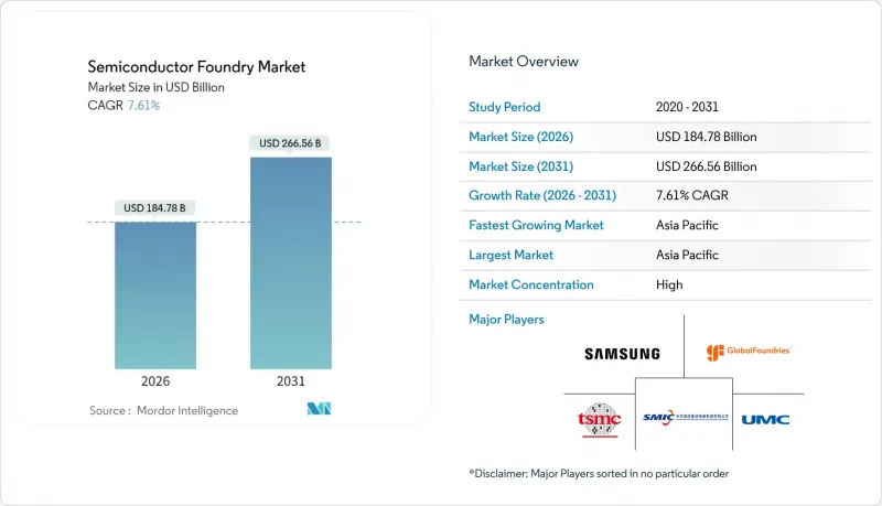
2026년의 세계 반도체 파운드리 시장 규모는 1,847억 8,000만 달러로 추정되며, 2025년 1,717억 2,000만 달러에서 성장하며, 2031년에는 2,665억 6,000만 달러에 달할 것으로 예측됩니다.
2026-2031년 연평균 7.61%의 연평균 복합 성장률(CAGR)을 보일 것으로 예측됩니다.

5nm 이하 공정에서 인공지능(AI)을 위한 컴퓨팅 수요의 급증, 성숙한 노드의 자동차용 칩에 대한 지속적인 수요, 그리고 정부의 강력한 인센티브 정책이 결합되어 이 분야의 기술적, 지역적 확장 범위를 확대하고 있습니다. 첨단 패키징 기술, 특히 칩렛과 3D 집적회로(3D IC)가 병행 수입원이 되고 있지만, 수자원 관리, 수출 규제 대응, EUV 장비 기술자 부족 등의 문제로 인해 단기적인 생산능력 확대가 제한되고 있습니다. 지정학적 경쟁의 격화로 북미, 유럽, 인도에서는 제조의 현지화가 진행되어 아시아태평양의 전통적 생산 우위가 점차 확산되고 있습니다. 그러나 그 주도적 지위는 흔들리지 않습니다. 현재 경쟁 구도는 5nm 이하 노드에서의 리더십, 비용 효율적인 28nm 제조 능력, 스타트업 기업을 위한 파운드리 서비스형 파운드리(Foundry-as-a-Service, FaaS) 제공에 초점이 맞추어져 있습니다.
세계 반도체 파운드리 시장 동향과 인사이트
5nm 이하 첨단 노드를 둘러싼 AI 가속기 경쟁
하이퍼스케일러와 칩 설계자들이 대규모 AI 모델 학습을 위해 경쟁하는 가운데, 5nm 이하 제조 능력은 틈새에서 주류로 이동했습니다. TSMC의 보고서에 따르면 2025년 2분기 웨이퍼 매출의 74%를 7nm 이하 노드가 차지하며 고객들이 밀도 우위를 중시하고 있음을 보여줍니다. 삼성의 2nm 게이트 올 어라운드 프로그램과 인텔의 1.4nm 로드맵은 업계 전체가 원자 단위의 미세화로 전환하고 있음을 입증하고 있습니다. 노드의 빠른 전환은 첨단 인터포저에 대한 수요를 가속화하고 있으며, 팹과 패키징 라인의 공동 최적화가 필수적입니다. 팹당 200억 달러가 넘는 높은 자본집약도는 진입 가능한 경쟁자를 제한하고, 공정 기술 우위가 점유율을 직접 결정하는 과점 시장을 공고히 하고 있습니다.
자동차 전동화에 따른 주류 칩 수요
전기자동차에는 두 가지 트랙의 실리콘이 필요합니다. 성숙 노드의 전력 관리 IC와 첨단 노드의 고성능 SoC입니다. 자동차 제조업체들이 중앙집중형 전자 아키텍처로 전환하면서 28nm와 45nm의 장기적인 생산량을 확보하여 주기적인 스마트폰 주문에 압박을 받는 팹에 안정적인 백필을 제공합니다. 긴 인증 주기와 엄격한 AEC-Q100 표준은 다년간의 생산 능력 예약을 유도하고, 성숙한 노드와 첨단 노드의 균형을 맞추는 파운드리의 매출 전망을 개선합니다. 테슬라의 맞춤형 칩 전략은 OEM이 전용 생산 능력 계약을 통해 공급을 확보하고 성능 차별화를 꾀할 수 있는 방법을 보여줍니다.
지정학적 수출규제의 불확실성
해외 생산 직접 제품 규정의 확대로 특정 국가로의 첨단 리소그래피 수출이 제한되면서 팹은 레거시 라인과 첨단 라인의 분리를 강요당하고 있습니다. 기업이 여러 관할권에서 중복된 장비 세트와 감사를 수행함에 따라 컴플라이언스 비용이 증가하고 있습니다. 미국의 압력에 따라 말레이시아가 강화한 반도체 정책은 동남아시아에 파급효과를 가져왔고, 현재 하이엔드 GPU의 운송은 장기적인 라이선스 심사를 유발하고 있습니다. 예측할 수 없는 규제는 특히 5nm 이하의 신규 프로젝트를 저해하고 단기적인 투자 사이클을 둔화시키고 있습니다.
부문 분석
2025년 기준 28nm 노드는 매출의 59.45%를 차지하며, 비용 중심의 대량 생산 장치용 반도체 파운드리 시장 규모의 기반이 되고 있습니다. 10nm 이하 노드는 출하량이 적지만 AI 및 HPC 수요의 견인에 힘입어 2031년까지 연평균 복합 성장률(CAGR) 9.05%를 나타낼 것으로 예측됩니다. 따라서 매출 구조는 양극화될 것입니다. 성숙 단계의 노드는 자동차 및 산업 분야에서 예측 가능한 현금 흐름을 확보하고, 최첨단 노드는 프리미엄 가격과 높은 이익률을 달성할 것입니다.
설비투자에 대한 규율은 여전히 매우 중요합니다. TSMC는 2025년에 2nm 공정의 위험 생산을 시작하고, 스마트폰 및 가속기 고객으로부터 선불금을 확보할 것입니다. 이에 대해 인텔과 삼성은 1.4nm와 2nm GAA(Gate All Around) 공정 개발 계획으로 맞불을 놓으며 자본 경쟁을 강화하고 있습니다. 한편, 16nm 및 14nm 노드는 네트워크용 실리콘의 비용 대비 성능 격차를 해소할 수 있습니다. 레거시 65nm 이상 공정은 수명주기이 긴 아날로그 및 RF 설계를 위해 계속 공급될 것이며, 휴대폰 수요 둔화에도 불구하고 팹 가동률이 양호한 수준으로 유지될 것입니다.
300mm 제조 장비로의 전환으로 1회당 다이 생산량이 증가하고, 단면 손실로 인한 폐기물이 감소했습니다. 이를 통해 2025년 반도체 파운드리 시장 점유율 68.10%를 확보할 수 있게 되었습니다. 신규 팹에서는 40nm 이하 공정에 300mm 장비를 표준으로 채택하므로 연평균 9.42%의 연평균 복합 성장률(CAGR)이 지속될 것으로 예측됩니다. 한편, 200mm는 MEMS, 파워 GaN, 특수 아날로그 분야에서 자리를 잡고 있으며, 미세화 및 화학적 특성이 300mm로의 전환을 어렵게 하고 있습니다.
규모의 경제 효과가 두드러집니다. 300mm 팹이월생산량 10만 웨이퍼에 도달하면, 설비 감가상각이 완료되는 시점에 200mm 웨이퍼 단가를 30% 낮출 수 있습니다. 그러나 150억-200억 달러의 진입장벽이 신규 진입을 제한하고 기존 기업의 우위를 강화하고 있습니다. 특수 기판에 의존하는 SiC, GaAs, 포토닉스 제품을 위한 150mm 전용 라인이 지속적으로 존재합니다.
지역별 분석
아시아태평양은 2025년 22.65%의 매출 점유율을 차지할 것으로 예상되며, 대만의 독보적인 첨단 노드 밀도와 한국의 수직 통합 생태계에 힘입어 2031년까지 연평균 복합 성장률(CAGR) 8.44%를 나타낼 것으로 전망됩니다. 대만의 2025년 2분기 매출 288억 7,000만 달러는 이 지역의 생산 규모가 얼마나 큰지 보여줍니다. 중국 SMIC는 수출 규제에 따라 28nm 이상 공정에 집중하는 반면, 말레이시아와 싱가포르는 미국의 규제 강화에도 불구하고 조립 및 테스트 분야를 심화시키고 있습니다.
북미는 CHIPS 법에 따라 제조 거점으로 재부상하고 있으며, 애리조나, 오하이오, 뉴욕의 착공으로 5nm급과 성숙 노드 모두에 대한 생산 능력이 추가될 예정입니다. 연방정부 보조금이 수십억 달러 규모의 프로젝트 리스크를 완화하고, 방산 분야 상계 계약이 최소 가동률을 보장합니다. 유럽은 자동차 등급 및 특수 아날로그 분야에 집중하고 있으며, 독일의 자동차 산업 클러스터와 네덜란드의 리소그래피 기술력을 활용하고 있습니다. EU의 자금 풀은 미국 패키지보다 규모가 작지만, 2030년까지 지역 생산량을 두 배로 늘리는 것을 목표로 하고 있습니다.
인도, 중동 및 아프리카 일부 지역에서는 조립, 테스트 및 설계 서비스에 대한 특혜를 통해 존재감을 드러내고 있습니다. 인도의 100억 달러 규모 프로그램, 마이크로닉스의 27억 5,000만 달러 규모의 ATMP(조립-테스트-제조 공정) 및 타타의 110억 달러 규모의 그린필드 공장 계획 유치. 2030년까지 1,000억-1,000억 달러에 육박하는 국내 수요를 내다보고 있습니다. 걸프 국가들은 경제 다각화를 위해 파운드리를 고려하고 있지만, 수자원 제약과 기술 격차가 진전을 저해하고 있습니다. 신흥 지역 전체가 공급망 단축과 지정학적 충격에 대한 헤지를 목표로 하고 있습니다.
기타 특전:
- 엑셀 형식 시장 예측(ME) 시트
- 애널리스트의 3개월간 지원
자주 묻는 질문
목차
제1장 서론
제2장 조사 방법
제3장 개요
제4장 시장 구도
제5장 시장 규모와 성장 예측
제6장 경쟁 구도
제7장 시장 기회와 향후 전망
KSA 26.03.06The global semiconductor foundry market size in 2026 is estimated at USD 184.78 billion, growing from 2025 value of USD 171.72 billion with 2031 projections showing USD 266.56 billion, growing at 7.61% CAGR over 2026-2031.
A combination of soaring artificial-intelligence compute needs at sub-5 nm, sustained demand for mature-node automotive chips, and intensive government incentives is widening both the technology and geographic footprint of the sector. Advanced packaging, especially chiplets and 3-D ICs, has become a parallel revenue engine, while water stewardship, export-control compliance, and EUV-tool talent shortages temper near-term capacity additions. Intensifying geopolitical competition is prompting North America, Europe, and India to localize fabrication, gradually diffusing Asia-Pacific's traditional production dominance without dislodging its leadership. Competitive dynamics now hinge on node leadership below 5 nm, cost-efficient 28 nm capacity, and foundry-as-a-service offerings targeting start-ups.
Global Semiconductor Foundry Market Trends and Insights
AI Accelerator Race for Less than 5 nm Advanced Nodes
Sub-5 nm capacity has moved from niche to mainstream as hyperscalers and chip designers race to train larger AI models. TSMC reported that 7 nm and finer nodes contributed 74% of wafer revenue in Q2 2025, underscoring the premium customers place on density leadership. Samsung's gate-all-around 2 nm program and Intel's 1.4 nm roadmap confirm an industry-wide pivot toward atomic-scale geometries. Rapid node migration is also fueling demand for advanced interposers, necessitating co-optimized fab and packaging lines. High capital intensity-often above USD 20 billion per fab-limits viable competitors and cements an oligopolistic market where process leadership directly dictates share.
Mainstream Chip Demand from Automotive Electrification
Electric vehicles require dual-track silicon: power-management ICs at mature nodes and high-compute SoCs at leading nodes. Automakers' shift to centralized electronic architectures locks in long-term 28 nm and 45 nm volumes, providing reliable backfill for fabs otherwise pressured by cyclical smartphone orders. Long qualification cycles and strict AEC-Q100 standards encourage multi-year capacity reservations, improving revenue visibility for foundries that balance mature and advanced nodes. Tesla's custom chip strategy illustrates how OEMs use dedicated capacity deals to secure supply and differentiate performance.
Geopolitical Export-Control Uncertainty
Expanded Foreign-Produced Direct Product rules restrict advanced lithography exports to specific countries, forcing fabs to segregate legacy and cutting-edge lines. Compliance costs rise as companies duplicate equipment sets and audits across jurisdictions. Malaysia's tighter chip policies under U.S. pressure show knock-on effects in Southeast Asia, where routing high-end GPUs now triggers lengthy license reviews. Unpredictable rule-making discourages green-field projects, particularly at 5 nm and below, muting near-term investment cycles.
Other drivers and restraints analyzed in the detailed report include:
- Defense Agencies' Push for Trusted Domestic Fabs
- Chiplets + 3-D IC Needing New Foundry Workflows
- Talent Crunch in Sub-3 nm EUV Maintenance
For complete list of drivers and restraints, kindly check the Table Of Contents.
Segment Analysis
In 2025, the 28 nm node generated 59.45% revenue, anchoring the semiconductor foundry market size for cost-sensitive, high-volume devices. Nodes finer than 10 nm, although smaller in shipment volume, will produce a 9.05% CAGR through 2031, reflecting AI and HPC pull-through. Revenue mix therefore bifurcates: mature nodes assure predictable automotive and industrial cash flows, while leading-edge nodes command premium pricing and margins.
Capex discipline remains pivotal. TSMC begins 2 nm risk production in 2025, drawing prepayments from smartphone and accelerator clients. Intel and Samsung respond with 1.4 nm and 2 nm gate-all-around timelines, intensifying capital races. Meanwhile, 16 nm and 14 nm nodes bridge cost-performance gaps for networking silicon. Legacy 65 nm and above still serve analog and RF designs with long lifecycles, keeping fabs running at healthy utilization even when handset demand softens.
The transition to 300 mm tooling lifted die output per run and cut edge-loss waste, enabling the segment to capture 68.10% of the semiconductor foundry market share in 2025. Growth persists at 9.42% CAGR as new fabs select 300 mm equipment by default for anything below 40 nm. In contrast, 200 mm remains entrenched in MEMS, power GaN, and niche analog where geometry or chemistry complicates 300 mm migration.
Economies of scale are stark. A 300 mm fab reaching 100,000 wafers-per-month can undercut 200 mm cost per die by 30% once fully depreciated. Yet the USD 15-20 billion entry fee restricts newcomers, reinforcing incumbent advantage. Specialized 150 mm lines persist for SiC, GaAs, and photonics products that rely on exotic substrates.
The Semiconductor Foundry Market Report is Segmented by Technology Node (10/7/5 Nm and Below, 16/14 Nm, 20 Nm, and More), Wafer Size (300 Mm, 200 Mm, <=150 Mm), Foundry Business Model (Pure-Play, IDM Foundry Services, Fab-Lite), Application (Consumer Electronics and Communication, Automotive, and More), and Geography (North America, South America, Europe, and More). The Market Forecasts are Provided in Terms of Value (USD).
Geography Analysis
Asia-Pacific captured 22.65% revenue in 2025 and is set for an 8.44% CAGR through 2031, propelled by Taiwan's unrivaled advanced-node density and South Korea's vertical integration ecosystems. Taiwan's Q2 2025 revenue of USD 28.87 billion underscores the region's throughput scale. China's SMIC concentrates on 28 nm and above amid export-tool restrictions, while Malaysia and Singapore reinforce assembly and test depth despite tighter U.S. compliance rules.
North America is re-emerging as a fabrication hub under the CHIPS Act, with groundbreakings in Arizona, Ohio, and New York adding both 5 nm class and mature-node capacity. Federal grants de-risk billion-dollar projects, and defense offsets guarantee baseline loadings. Europe focuses on automotive-grade and specialty analog, leveraging Germany's auto cluster and the Netherlands' lithography prowess. EU funding pools, though smaller than U.S. packages, aim to double regional output by 2030.
India, the Middle East, and pockets of Africa are staking claims via assembly, test, and design-service incentives. India's USD 10 billion program attracted Micron's USD 2.75 billion ATMP and Tata's USD 11 billion green-field fab plans, targeting domestic demand approaching USD 100-110 billion by 2030. Gulf countries explore foundries for economic diversification, but water constraints and skills gaps temper speed. Collectively, new geographies aim to shorten supply chains and hedge geopolitical shocks.
- Taiwan Semiconductor Manufacturing Co. Ltd. (TSMC)
- Samsung Electronics Co. Ltd. (Samsung Foundry)
- GlobalFoundries Inc.
- United Microelectronics Corp. (UMC)
- Semiconductor Manufacturing International Corp. (SMIC)
- Intel Corp. (Intel Foundry Services)
- Tower Semiconductor Ltd.
- STMicroelectronics N.V.
- Powerchip Semiconductor Manufacturing Corp. (PSMC)
- Vanguard International Semiconductor Corp.
- Hua Hong Semiconductor Ltd.
- X-FAB Silicon Foundries SE
- ASE Group
- Dongbu HiTek Co. Ltd.
- Renesas Electronics Corp.
- JCET Group
- Amkor Technology
- SkyWater Technology Inc.
- VIS Semiconductor Co. Ltd.
- PSMC Group (Nexchip)
Additional Benefits:
- The market estimate (ME) sheet in Excel format
- 3 months of analyst support
TABLE OF CONTENTS
1 INTRODUCTION
- 1.1 Study Assumptions and Market Definition
- 1.2 Scope of the Study
2 RESEARCH METHODOLOGY
3 EXECUTIVE SUMMARY
4 MARKET LANDSCAPE
- 4.1 Market Overview
- 4.2 Market Drivers
- 4.2.1 Mainstream chip demand from automotive electrification
- 4.2.2 IoT-edge proliferation requiring mature?node capacity
- 4.2.3 AI accelerator race for Less than 5 nm advanced nodes
- 4.2.4 Chiplets + 3D IC needing new foundry workflows
- 4.2.5 Defense agencies push for trusted domestic fabs
- 4.2.6 Foundry-as-a-Service model for start-ups
- 4.3 Market Restraints
- 4.3.1 Geopolitical export-control uncertainty
- 4.3.2 Capex inflation and long pay-back periods
- 4.3.3 Water-use permits limiting mega-fabs
- 4.3.4 Talent crunch in sub-3 nm EUV maintenance
- 4.4 Industry Value Chain Analysis
- 4.5 Regulatory Landscape
- 4.6 Technological Outlook
- 4.7 Foundry Capacity Utilization Trends
- 4.8 Porter's Five Forces Analysis
- 4.8.1 Bargaining Power of Suppliers
- 4.8.2 Bargaining Power of Buyers
- 4.8.3 Threat of New Entrants
- 4.8.4 Threat of Substitutes
- 4.8.5 Intensity of Competitive Rivalry
- 4.9 Impact of Macroeconomic Factors on the Market
5 MARKET SIZE AND GROWTH FORECASTS (VALUE)
- 5.1 By Technology Node
- 5.1.1 10/7/5 nm and below
- 5.1.2 16/14 nm
- 5.1.3 20 nm
- 5.1.4 28 nm
- 5.1.5 45/40 nm
- 5.1.6 65 nm and above
- 5.2 By Wafer Size
- 5.2.1 300 mm
- 5.2.2 200 mm
- 5.2.3 ?150 mm
- 5.3 By Foundry Business Model
- 5.3.1 Pure-play
- 5.3.2 IDM Foundry Services
- 5.3.3 Fab-lite
- 5.4 By Application
- 5.4.1 Consumer Electronics and Communication
- 5.4.2 Automotive
- 5.4.3 Industrial and IoT
- 5.4.4 High-Performance Computing (HPC)
- 5.4.5 Other Applications
- 5.5 By Geography
- 5.5.1 North America
- 5.5.1.1 United States
- 5.5.1.2 Canada
- 5.5.1.3 Mexico
- 5.5.2 South America
- 5.5.2.1 Brazil
- 5.5.2.2 Argentina
- 5.5.2.3 Rest of South America
- 5.5.3 Europe
- 5.5.3.1 Germany
- 5.5.3.2 United Kingdom
- 5.5.3.3 France
- 5.5.3.4 Italy
- 5.5.3.5 Rest of Europe
- 5.5.4 Asia-Pacific
- 5.5.4.1 China
- 5.5.4.2 Japan
- 5.5.4.3 South Korea
- 5.5.4.4 India
- 5.5.4.5 Rest of Asia-Pacific
- 5.5.5 Middle East
- 5.5.5.1 Saudi Arabia
- 5.5.5.2 United Arab Emirates
- 5.5.5.3 Rest of Middle East
- 5.5.6 Africa
- 5.5.6.1 South Africa
- 5.5.6.2 Rest of Africa
- 5.5.1 North America
6 COMPETITIVE LANDSCAPE
- 6.1 Market Concentration
- 6.2 Strategic Moves
- 6.3 Market Share Analysis
- 6.4 Company Profiles (includes Global level Overview, Market level Overview, Core Segments, Financials as available, Strategic Information, Market Rank/Share, Products and Services, Recent Developments)
- 6.4.1 Taiwan Semiconductor Manufacturing Co. Ltd. (TSMC)
- 6.4.2 Samsung Electronics Co. Ltd. (Samsung Foundry)
- 6.4.3 GlobalFoundries Inc.
- 6.4.4 United Microelectronics Corp. (UMC)
- 6.4.5 Semiconductor Manufacturing International Corp. (SMIC)
- 6.4.6 Intel Corp. (Intel Foundry Services)
- 6.4.7 Tower Semiconductor Ltd.
- 6.4.8 STMicroelectronics N.V.
- 6.4.9 Powerchip Semiconductor Manufacturing Corp. (PSMC)
- 6.4.10 Vanguard International Semiconductor Corp.
- 6.4.11 Hua Hong Semiconductor Ltd.
- 6.4.12 X-FAB Silicon Foundries SE
- 6.4.13 ASE Group
- 6.4.14 Dongbu HiTek Co. Ltd.
- 6.4.15 Renesas Electronics Corp.
- 6.4.16 JCET Group
- 6.4.17 Amkor Technology
- 6.4.18 SkyWater Technology Inc.
- 6.4.19 VIS Semiconductor Co. Ltd.
- 6.4.20 PSMC Group (Nexchip)
7 MARKET OPPORTUNITIES AND FUTURE OUTLOOK
- 7.1 White-space and Unmet-need Assessment
