


|
시장보고서
상품코드
1940697
반도체 리소그래피 장비 : 시장 점유율 분석, 업계 동향과 통계, 성장 예측(2026-2031년)Semiconductor Lithography Equipment - Market Share Analysis, Industry Trends & Statistics, Growth Forecasts (2026 - 2031) |
||||||
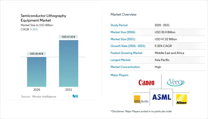
반도체 리소그래피 장비 시장은 2025년 278억 달러에서 2026년에는 304억 달러에 이르고, 2026-2031년 CAGR 9.35%로 성장을 지속하여 2031년까지 475억 2,000만 달러에 달할 것으로 예측됩니다.
이러한 성장 모멘텀은 극자외선(EUV) 및 향후 고NA EUV 플랫폼으로의 전환, 인공지능 서버의 급증, 그리고 더 높은 패터닝 정확도를 요구하는 수조 트랜지스터 규모의 그래픽 가속기에 기인합니다. 아시아태평양은 대만의 파운드리 우위와 한국의 4,710억 달러 규모의 메가 클러스터 계획에 힘입어 제조 역량 확대의 핵심 지역으로 자리매김하고 있습니다. 딥 자외선(DUV) 장비는 여전히 성숙한 노드의 기반으로서 중요하지만, 고나노 EUV 장비의 수주 파이프라인은 생태계가 1nm 이하 생산으로 빠르게 전환하고 있음을 보여줍니다. 설비 투자 집중도와 수출 규제 대응이 보급의 주요 장벽이 되고 있지만, 정부 보조금, 패키징 기술 혁신, 에너지 절약형 장비 설계가 결합되어 첨단 노광 시스템의 적용 범위를 확대하고 있습니다.
세계 반도체 리소그래피 장비 시장 동향과 인사이트
미세화 공정으로 EUV 도입 촉진
트랜지스터 밀도 증가로 EUV만이 달성할 수 있는 7nm 이하의 미세화가 요구되고 있습니다. TSMC는 2030년까지 1nm 공정 양산을 준비하는 가운데, 신주 공장에 고NA 노광장비의 첫 선을 보였습니다. ASML의 EXE 플랫폼은 아나모픽 광학을 통해 8nm 해상도를 달성하고, 기존 NXE 모델 대비 40% 향상된 이미징 콘트라스트를 구현합니다. 연구팀은 5nm 선간격 간섭 노광을 실현하여 로드맵을 크게 밑도는 능력을 확인했습니다. 서버급 프로세서는 2,000억 트랜지스터로 두 배로 증가할 것으로 예상되며, 리소그래피의 처리 능력에 대한 수요가 확대되고 있습니다. 이러한 이정표는 옹스트롬 단위의 미세화를 향한 빠른 속도를 강조하고, 고 NA 장비를 설비 투자의 최우선 순위로 삼고 있음을 보여줍니다.
최첨단 칩에 대한 AI 및 데이터센터 수요
인공지능 서버에는 2조 개 이상의 트랜지스터가 탑재된 멀티칩 GPU가 필요합니다. 반도체 매출은 2030년까지 1조 달러를 넘어설 것으로 예상되며, AI 가속기와 고대역폭 메모리가 주요 성장 동력이 될 것입니다. CoWoS와 같은 첨단 패키징 기술은 재배선층의 리소그래피 오버레이 정밀도를 더욱 엄격하게 요구합니다. 삼성의 이기종 통합 로드맵과 TSMC의 CoWoS 생산능력 확대에 따라 대형 패널 노광장비에 대한 긴급 주문이 잇따르고 있습니다. 수십만 개의 GPU를 보유한 아부다비의 1-5GW 규모의 AI 컴퓨팅 클러스터는 새로운 지역이 설비투자 사이클에 진입할 조짐을 보이고 있습니다.
EUV 노광 장비의 초고액 설비 투자
ASML의 고NA 장비는 대당 3.8억 달러로 초기 EUV 플랫폼의 2배에 달하는 가격입니다. 클린룸 재구축, 방진 대책, 메가와트급 전력 및 냉각 설비로 인해 총소유비용은 더욱 증가합니다. 2025년 말까지 전 세계에 설치될 고NA 장비는 20개 미만이 될 것으로 예상되며, 중견 팹은 옹스트롬 경쟁에서 밀려날 것으로 보입니다. 오키나와과학기술대학원대학교의 조사에서는 2장의 거울을 이용한 프로젝터와 20W의 광원을 제안하고 있으며, 이를 통해 전력 소비를 90% 절감할 수 있는 가능성을 시사하고 있어 향후 설비투자 부담의 경감이 기대됩니다.
부문 분석
2025년 DUV 플랫폼은 반도체 리소그래피 장비 시장 점유율의 56.10%를 유지하며, 성숙 노드 및 비용 중심 라인에서 그 중요성을 보여주었습니다. 고NA EUV는 현재 반도체 리소그래피 장비 시장 규모에서 차지하는 비중은 작지만, 단일 노광에 의한 1nm 이미징이 양산화되는 2031년까지 연평균 복합 성장률(CAGR) 10.54%를 나타낼 것으로 예측됩니다. ASML의 EXE 시리즈에 탑재된 0.55 NA 아나모픽 프로젝션 기술은 초점 깊이를 개선하고, 기존에는 4중 패터닝 없이는 달성할 수 없었던 결함 밀도 목표를 달성할 수 있게 합니다. Imec이 20nm 피치 금속 배선에서 90%의 전기적 수율을 달성한 것은 양산 준비가 완료되었음을 입증합니다.
기존 EUV는 5nm 로직, 낸드플래시, DRAM 리프레시에 여전히 필수적이며, 0.33 NA에서 멀티패터닝을 통해 허용 가능한 오버레이를 얻을 수 있습니다. 이미 많은 팹에서 상각이 완료된 심자외선 침지노광은 아날로그, RF, MEMS 공정에서 다이 단가의 우위를 유지하고 있습니다. 캐논의 나노임프린트 파일럿 라인과 니콘의 침지노광 기술 강화는 틈새 시장에서의 경쟁을 시사하고 있지만, ASML의 레티클 포맷을 중심으로 한 생태계에 대한 의존도가 플랫폼 우위를 뒷받침하고 있습니다.
지역별 분석
2025년 아시아태평양의 67.60%의 점유율은 대만, 한국, 일본, 일본, 중국 본토에 집적된 로직 메모리 메가팹을 반영하고 있습니다. 한국의 4,710억 달러 규모의 클러스터에 여러 EUV 장비가 추가되었고, 일본 정부의 지원책은 TSMC를 구마모토 2단계 공장 건설로 유인하고 있습니다. 중국은 수출 규제에도 불구하고 국내 리소그래피 프로젝트 확대에 따라 2024년 전체 팹 장비에 490억 달러를 지출했습니다.
북미는 2위, CHIPS법 공동 투자로 인텔, TSMC, 삼성의 미국 프로젝트 총액 2,000억 달러 돌파. 애리조나 트윈팹 캠퍼스에서만 예측 기간 동안 25대 이상의 EUV 노광기를 도입할 예정입니다. 오레곤, 오하이오, 텍사스의 팹 클러스터는 지리적 중복성을 확대하고 지역 장비 서비스 수요를 강화합니다.
중동 및 아프리카은 현재 규모가 작지만 12.48%의 연평균 복합 성장률(CAGR)을 보이고 있습니다. 사우디의 10억 사우디 리얄 규모의 벤처 펀드가 국가 반도체 허브를 지원하고, UAE의 데이터센터 프로젝트는 현지의 첨단 패키징 능력을 필요로 합니다. 정부 간 기술이전 협정은 타임라인 단축을 촉진하지만, 노동력과 공급망의 깊이는 여전히 개발의 병목현상이 되고 있습니다.
기타 특전:
- 엑셀 형식 시장 예측(ME) 시트
- 애널리스트의 3개월 지원
자주 묻는 질문
목차
제1장 서론
제2장 조사 방법
제3장 주요 요약
제4장 시장 구도
제5장 시장 규모와 성장 예측
제6장 경쟁 구도
제7장 시장 기회와 향후 전망
LSH 26.03.10The semiconductor lithography equipment market is expected to grow from USD 27.8 billion in 2025 to USD 30.4 billion in 2026 and is forecast to reach USD 47.52 billion by 2031 at 9.35% CAGR over 2026-2031.

Momentum stems from the shift toward extreme ultraviolet (EUV) and forthcoming High-NA EUV platforms, the surge in artificial-intelligence servers, and multi-trillion-transistor graphics accelerators that demand denser patterning precision. Asia-Pacific remains the fulcrum of manufacturing capacity expansions, led by Taiwan's foundry dominance and South Korea's USD 471 billion mega-cluster program. Deep-ultraviolet (DUV) tools still anchor mature nodes, but the pipeline of High-NA EUV orders shows how quickly the ecosystem is pivoting toward sub-1 nm production. Capital-expenditure intensity and export-control compliance are the main brakes on diffusion, yet government subsidies, packaging innovations, and energy-efficient tool designs together widen the addressable base for advanced exposure systems.
Global Semiconductor Lithography Equipment Market Trends and Insights
Shrinking Process Nodes Drive EUV Adoption
Growing transistor density forces sub-7 nm geometries that only EUV can achieve. TSMC recorded first light on a High-NA tool in Hsinchu as it prepares 1 nm mass output by 2030. ASML's EXE platform reaches 8 nm resolution with anamorphic optics, a 40% imaging-contrast jump over prior NXE models. Research teams demonstrated 5 nm line-space interference printing, confirming far-below-roadmap capability. Server-class processors are projected to double to 200 billion transistors, magnifying lithography throughput needs. These milestones underline a rapid cadence toward angstrom dimensions that places High-NA tools at the center of capex priorities.
AI and Data-Center Demand for Leading-Edge Chips
Artificial-intelligence servers require multi-chiplet GPUs pushing past 2 trillion transistors. Semiconductor revenue is modeled to top USD 1 trillion by 2030, with AI accelerators and high-bandwidth memory as primary growth engines. Advanced packaging formats such as CoWoS intensify lithography overlay accuracy for redistribution layers. Samsung's heterogeneous-integration roadmap and TSMC's CoWoS capacity ramp have driven rush orders for large-panel exposure tools. Abu Dhabi's 1-5 GW AI compute cluster, featuring hundreds of thousands of GPUs, signals new geographies entering the capex cycle.
Ultra-High Capex of EUV Scanners
ASML's High-NA units list at USD 380 million each, double the cost of early EUV platforms. Total cost of ownership multiplies after clean-room reconfiguration, vibration isolation, and megawatt-class power-and-cooling utilities. Fewer than 20 High-NA machines are likely installed worldwide by end-2025, leaving mid-tier fabs locked out of the angstrom race. Research at the Okinawa Institute proposes a two-mirror projector and a 20-W source that could shrink power draw by 90%, hinting at future capex relief.
Other drivers and restraints analyzed in the detailed report include:
- Government Fab Subsidies Drive Equipment Investment
- Advanced-Packaging Boom Accelerates Equipment Demand
- Export-Control Restrictions to China
For complete list of drivers and restraints, kindly check the Table Of Contents.
Segment Analysis
In 2025, DUV platforms maintained 56.10% semiconductor lithography equipment market share, underlining their role in mature-node and cost-sensitive lines. High-NA EUV, although a smaller slice of the semiconductor lithography equipment market size today, is forecast to grow 10.54% CAGR through 2031 as single-exposure 1 nm imaging becomes a production reality. The 0.55 NA anamorphic projection inside ASML's EXE series improves depth-of-focus, enabling defect-density targets previously unattainable without quadruple patterning. Imec's 90% electrical yield on 20 nm pitch metal lines corroborates readiness for volume runs.
Conventional EUV remains indispensable for 5 nm logic, NAND flash, and DRAM refreshes, where 0.33 NA offers acceptable overlay with multi-patterning. Deep-UV immersion, already fully depreciated at many fabs, keeps the cost-per-die edge for analog, RF, and MEMS flows. Canon's nano-imprint pilot lines and Nikon's immersion enhancements signal niche competitive threats, yet ecosystem lock-in around ASML reticle formats sustains its platform moat.
The Semiconductor Lithography Machine Manufacturers Market is Segmented by Type (Deep Ultraviolet Lithography and Extreme Ultraviolet Lithography), Application (Advanced Packaging, MEMS Devices, and LED Devices), and Geography (North America, Europe, and More). The Market Forecasts are Provided in Terms of Value (USD).
Geography Analysis
Asia-Pacific's 67.60% share in 2025 reflects the agglomeration of logic and memory megafabs across Taiwan, South Korea, Japan, and mainland China. South Korea's USD 471 billion cluster will add multiple EUV suites, while Japan's government incentives lure TSMC into second-phase Kumamoto construction. China, despite export curbs, still spent USD 49 billion on overall fab tools in 2024 as domestic lithography projects scale.
North America ranks second, fueled by CHIPS Act co-funding that pushes combined Intel, TSMC, and Samsung U.S. projects past USD 200 billion. Arizona's twin-fab campus alone will deploy more than 25 EUV scanners over the forecast horizon. Fab clusters in Oregon, Ohio, and Texas broaden geographic redundancy and strengthen regional tool-service demand.
The Middle East and Africa, though small today, show a 12.48% CAGR. Saudi Arabia's SAR 1 billion venture fund underpins the National Semiconductor Hub, while UAE data-center projects necessitate local advanced-packaging capacity. Government-to-government technology-transfer accords expedite timeline compression, but workforce and supply-chain depth remain developmental bottlenecks.
- ASML Holding N.V.
- Nikon Corporation
- Canon Inc.
- Shanghai Micro Electronics Equipment (Group) Co., Ltd.
- SUSS MicroTec SE
- EV Group
- Veeco Instruments Inc.
- Onto Innovation Inc.
- JEOL Ltd.
- Neutronix Quintel Inc.
- Mycronic AB
- NuFlare Technology Inc.
- Ushio Inc.
- Ultratech (Veeco)
- Mapper Lithography B.V.
- Visitech AS
- KLA Corporation
- MKS Instruments (Newport)
- Inpria Corp.
- Tamarack Scientific Co.
Additional Benefits:
- The market estimate (ME) sheet in Excel format
- 3 months of analyst support
TABLE OF CONTENTS
1 INTRODUCTION
- 1.1 Study Assumptions and Market Definition
- 1.2 Scope of the Study
2 RESEARCH METHODOLOGY
3 EXECUTIVE SUMMARY
4 MARKET LANDSCAPE
- 4.1 Market Overview
- 4.2 Market Drivers
- 4.2.1 Shrinking process nodes drive EUV adoption
- 4.2.2 AI and data-center demand for leading-edge chips
- 4.2.3 Government fab subsidies (e.g., CHIPS Act)
- 4.2.4 Advanced-packaging boom (2.5D/3D IC)
- 4.2.5 High-NA EUV refresh accelerates tool cycles
- 4.2.6 Compound-semiconductor lithography demand
- 4.3 Market Restraints
- 4.3.1 Ultra-high capex of EUV scanners
- 4.3.2 Sub-system supply-chain bottlenecks
- 4.3.3 Sustainability and energy-use pressures
- 4.3.4 Export-control restrictions to China
- 4.4 Value Chain Analysis
- 4.5 Regulatory Landscape
- 4.6 Technological Outlook
- 4.7 Porter's Five Forces Analysis
- 4.7.1 Threat of New Entrants
- 4.7.2 Bargaining Power of Suppliers
- 4.7.3 Bargaining Power of Buyers
- 4.7.4 Threat of Substitutes
- 4.7.5 Competitive Rivalry
- 4.8 Pricing Analysis
- 4.9 Impact of Macroeconomic Factors
5 MARKET SIZE AND GROWTH FORECASTS (VALUE)
- 5.1 By Lithography Type
- 5.1.1 Deep Ultraviolet (DUV)
- 5.1.2 Extreme Ultraviolet (EUV)
- 5.1.3 High-NA EUV
- 5.2 By Application
- 5.2.1 Advanced Packaging
- 5.2.2 MEMS Devices
- 5.2.3 LED Devices
- 5.2.4 Power and Compound Semiconductors
- 5.3 By End-User
- 5.3.1 Pure-play Foundries
- 5.3.2 Integrated Device Manufacturers (IDMs)
- 5.3.3 Outsourced Semiconductor Assembly and Test (OSAT)
- 5.4 By Geography
- 5.4.1 North America
- 5.4.1.1 United States
- 5.4.1.2 Canada
- 5.4.1.3 Mexico
- 5.4.2 South America
- 5.4.2.1 Brazil
- 5.4.2.2 Argentina
- 5.4.2.3 Rest of South America
- 5.4.3 Europe
- 5.4.3.1 Germany
- 5.4.3.2 United Kingdom
- 5.4.3.3 France
- 5.4.3.4 Italy
- 5.4.3.5 Spain
- 5.4.3.6 Russia
- 5.4.3.7 Rest of Europe
- 5.4.4 Asia Pacific
- 5.4.4.1 China
- 5.4.4.2 Japan
- 5.4.4.3 India
- 5.4.4.4 South Korea
- 5.4.4.5 South East Asia
- 5.4.4.6 Rest of Asia Pacific
- 5.4.5 Middle East and Africa
- 5.4.5.1 Middle East
- 5.4.5.1.1 Saudi Arabia
- 5.4.5.1.2 United Arab Emirates
- 5.4.5.1.3 Turkey
- 5.4.5.1.4 Rest of Middle East
- 5.4.5.2 Africa
- 5.4.5.2.1 South Africa
- 5.4.5.2.2 Nigeria
- 5.4.5.2.3 Rest of Africa
- 5.4.5.1 Middle East
- 5.4.1 North America
6 COMPETITIVE LANDSCAPE
- 6.1 Market Concentration
- 6.2 Strategic Moves
- 6.3 Market Share Analysis
- 6.4 Company Profiles (includes Global level Overview, Market level overview, Core Segments, Financials as available, Strategic Information, Market Rank/Share for key companies, Products and Services, and Recent Developments)
- 6.4.1 ASML Holding N.V.
- 6.4.2 Nikon Corporation
- 6.4.3 Canon Inc.
- 6.4.4 Shanghai Micro Electronics Equipment (Group) Co., Ltd.
- 6.4.5 SUSS MicroTec SE
- 6.4.6 EV Group
- 6.4.7 Veeco Instruments Inc.
- 6.4.8 Onto Innovation Inc.
- 6.4.9 JEOL Ltd.
- 6.4.10 Neutronix Quintel Inc.
- 6.4.11 Mycronic AB
- 6.4.12 NuFlare Technology Inc.
- 6.4.13 Ushio Inc.
- 6.4.14 Ultratech (Veeco)
- 6.4.15 Mapper Lithography B.V.
- 6.4.16 Visitech AS
- 6.4.17 KLA Corporation
- 6.4.18 MKS Instruments (Newport)
- 6.4.19 Inpria Corp.
- 6.4.20 Tamarack Scientific Co.
7 MARKET OPPORTUNITIES AND FUTURE OUTLOOK
- 7.1 White-space and Unmet-Need Assessment
