|
시장보고서
상품코드
1940700
다이싱 장비 : 시장 점유율 분석, 업계 동향과 통계, 성장 예측(2026-2031년)Dicing Equipment - Market Share Analysis, Industry Trends & Statistics, Growth Forecasts (2026 - 2031) |
||||||
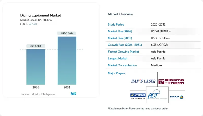
다이싱 장비 시장 규모는 2025년 8억 3,000만 달러에서2026년에는 8억 8,000만 달러에 이를 것으로 예측됩니다.
2031년에는 12억 달러에 달할 것으로 예상되며, 2026-2031년 연평균 복합 성장률(CAGR) 6.33%로 성장할 것으로 전망됩니다.

반도체 백엔드 제조 분야, 특히 박형 웨이퍼, 첨단 패키징 기술, 광대역 갭 전력 소자에 대한 견고한 투자가 이러한 꾸준한 성장을 뒷받침하고 있습니다. 전기자동차, 재생에너지, AI 워크로드에 대한 수요가 증가함에 따라 칩 제조업체들은 고수율 다이 분리, 서브마이크로미터 단위의 위치 결정 정확도, 오염 제어 가공 공정, 통합 검사 기능을 갖춘 시스템을 우선시하고 있습니다. 3D 및 이종 집적화로의 지속적인 전환으로 인해, 칩을 최소화하고 좁은 거리를 구현하는 플라즈마 및 레이저 다이싱 장비에 대한 수요가 증가하고 있습니다. 한편, 자동화의 고도화는 팹이 노동력 부족을 보완하고 공정 전환 시간을 단축하며 종합 설비 효율(OEE)을 향상시키는 데 기여하고 있습니다. 미국, 유럽, 동아시아공급망 지역화 프로그램은 새로운 지역 수요 거점을 창출하고 있지만, 희토류 레이저 소스를 둘러싼 지속적인 지정학적 마찰과 슬러리 폐기에 대한 엄격한 규제로 인해 자본 집약도는 여전히 높은 수준을 유지하고 있습니다.
세계 다이싱 장비 시장 동향 및 인사이트
고정밀 모션 시스템의 기술적 진보
최근 모션 제어 기술의 혁신으로 이기종 통합 라인에 필수적인 서브마이크로미터 단위의 스테이지 정밀도를 구현할 수 있게 되었습니다. 예를 들어, DISCO의 DFD6370 플랫폼은 330×330mm 기판을 처리하면서 절단 깊이를 ±1μm 이내로 유지하는 선택 가능한 높이 센서를 채택하여 패널 레벨 패키징에서 우위를 점하고 있습니다. 액티브 댐핑, 폐쇄 루프 로봇 기술, 비전 가이드를 통한 위치 결정으로 진동과 열 드리프트를 더욱 감소시켜 취성 실리콘 카바이드 웨이퍼 가공 시 높은 수율을 달성할 수 있습니다. 온보드 측정 기능을 갖춘 다축 스테이지를 통합하는 벤더는 절단, 세척, 검사를 단일 흐름으로 결합한 턴키 방식의 싱글레이션 셀을 제공하여 핸들링 결함과 사이클 타임을 줄입니다.
첨단 로직 메모리 공장에서 수요 급증
SEMI의 예측에 따르면, 2025년부터 2027년까지 300mm 팹에 대한 총 설비 투자액은 4,000억 달러에 달할 것으로 예상되며, 그 중 주조가 2,300억 달러를 차지할 것으로 예측됩니다. 새로운 극자외선(EUV) 공정 노드 및 3D 적층 DRAM 라인의 도입으로 인해, 후면 오염의 위험이 증가하고 있으며, 팹에서는 정전기 억제 기능 및 밀폐형 칩 회수 기능을 갖춘 다이싱 장비의 채택이 요구되고 있습니다. 특히 TSMC, 삼성, 중국 내 파운드리의 생산능력 확대가 가속화되고 있는 가운데, 장비 공급업체에게는 신속한 장비 납품 및 현장 서비스망 확충이 중요한 조달 판단 기준이 되고 있습니다.
슬러리 및 화학물질 폐기 규제 강화
ISO 14644 클린룸 표준의 개정과 새로운 PFAS 규정에 따라 팹은 폐수 루프의 개조, 불소 화합물 제거 시스템 설치, 폐쇄 루프 냉각수 채택을 요구하고 있습니다. 다이싱 셀에 재활용 모듈과 실시간 입자 모니터를 내장한 벤더는 고객이 규제 기준을 충족시키면서 광열비를 절감할 수 있도록 돕고 있습니다. 다만, 추가 설비 비용과 시설 개보수로 인해 구매 결정이 늦어지는 경우도 볼 수 있습니다.
부문 분석
2025년 기준 다이싱 장비 시장의 46.10%를 블레이드 시스템이 차지하고 있습니다. 웨이퍼 당 비용 우위와 성숙한 서비스 네트워크가 대량 생산 로직 메모리 라인에 적합하기 때문입니다. 그러나 50µ&m 미만의 웨이퍼가 보급되면서 레이저 부문은 6.53%의 연평균 복합 성장률(CAGR)로 성장하고 있습니다. 이는 기존의 블레이드가 보장할 수 없는 끊김 없는 싱글레이션(조각화)이 요구되기 때문입니다. 파나소닉의 APX300 플라즈마 플랫폼은 300mm 웨이퍼에서 20µm의 거리 폭을 실현하여 플라즈마 레이저 툴의 성능 향상을 입증했습니다. 블레이드에 의한 거친 절단과 레이저 마무리를 결합한 하이브리드 라인도 보급되어, 처리량과 다이 강도의 균형을 실현하고 있습니다.
레이저 광학, 희토류 정렬 부품, 수 kW급 전원장치의 추가 비용은 여전히 가격에 민감한 팹에서 도입을 제한하고 있습니다. 그러나 다이-투-패키지 수직 배선 및 취성 SiC 기판이 주류가 되는 분야에서는 초기 투자비용이 높지만, 폐기율 감소와 설계 규칙의 강화로 인해 상쇄됩니다. 예측 기간에는 초고속 펄스 성형 기술과 오토포커스 광학계의 지속적인 연구개발로 장비 가동률이 향상되고, 웨이퍼 단가의 원가 차이가 점차 축소될 것으로 예측됩니다.
반도체 업계는 더 큰 웨이퍼 포맷으로 전환하고 있으며, 450mm 이상의 웨이퍼는 2031년까지 연평균 복합 성장률(CAGR) 6.38%로 성장하여 2025년 37.55%의 시장 점유율을 차지한 300mm 웨이퍼에 근접할 것으로 예측됩니다. 첨단 패키징 응용 분야, 특히 패널 레벨 패키징 공정에서 더 큰 기판 처리 능력에 대한 수요가 증가하고 있습니다. 디스코의 DFD6370은 최대 330×330mm의 공작물을 처리할 수 있으며, 기존의 웨이퍼 처리와 새로운 대형화 요구 사이의 간극을 메울 수 있습니다.
200mm 이하의 소형 웨이퍼는 MEMS 디바이스, 파워 반도체 등 특수 용도에서 여전히 중요한 위치를 차지하고 있습니다. 기판 비용 및 공정 최적화 측면에서 확립된 포맷이 유리한 분야입니다. 200mm 부문은 성숙 노드 확대와 자동차용 반도체 수요의 수혜를 받고 있으며, 150mm 웨이퍼는 화합물 반도체 및 레거시 디바이스 생산의 틈새 용도에 활용되고 있습니다. 그러나 기판당 다이 수율 향상 및 단위 처리 비용 절감 등 대형 웨이퍼의 경제적 우위가 포맷 전환을 촉진하고 있습니다. SEMI의 'World Fab Forecast'는 2027년까지 가동될 가능성이 높은 79곳의 제조시설을 선정했으며, 이 중 상당수가 혼합 웨이퍼 사이즈 대응 능력을 갖추고 있습니다. 단일 플랫폼 내에서 여러 웨이퍼 포맷을 지원하는 확장 가능한 핸들링 시스템을 개발하는 장비 제조업체는 이러한 진화하는 환경에서 우위를 점할 수 있습니다.
지역별 분석
아시아태평양은 대만, 한국, 일본, 중국 본토에 뿌리내린 제조 클러스터에 힘입어 2025년에도 다이싱 장비 시장에서 42.55%의 점유율을 유지할 것으로 예측됩니다. 일본 정부의 총 3조 9,000억 엔(260억 달러)의 보조금 지원은 일본의 부활을 뒷받침하고 정밀 모션 벤더와 자동화 통합업체에 대한 수주를 촉진하고 있습니다. 중국의 OSAT(위탁 조립 서비스) 업체들은 자체 설계한 AI 가속기의 수율 향상을 위해 플라즈마 다이싱 라인 도입에 박차를 가하고 있습니다. 한편, 동남아시아 국가에서는 조립 업무의 파급 효과로 인해 중형 블레이드 다이서 수요가 발생하고 있습니다.
북미의 CHIPS 법은 500억 달러가 넘는 특혜를 허용하고 있으며, 애리조나, 텍사스, 뉴욕주 북부의 신규 공장을 2026년 이후 새로운 조달 거점으로 탈바꿈시키고 있습니다. 이들 거점에서는 숙련된 인력 부족을 보완하기 위해 예지보전 분석 기능을 갖춘 완전 자동화 블레이드/레이저 셀을 우선적으로 도입하고 있습니다.
유럽의 칩 법은 대륙의 생산 능력에 470억 달러를 투입하고, 독일과 프랑스의 프로젝트가 EV 공급망용 실리콘 카바이드 파워 일렉트로닉스를 주도하고 있습니다. 아시아 생산량에는 미치지 못하지만, EU 팹의 엄격한 환경 기준은 폐쇄형 슬러리 및 저수소비 플라즈마 다이싱 시스템의 도입을 가속화하여 이 지역의 평균 판매 가격(ASP)을 높이고 있습니다.
기타 특전:
- 엑셀 형식 시장 예측(ME) 시트
- 애널리스트의 3개월간 지원
자주 묻는 질문
목차
제1장 서론
제2장 조사 방법
제3장 주요 요약
제4장 시장 구도
제5장 시장 규모와 성장 예측
제6장 경쟁 구도
제7장 시장 기회와 향후 전망
LSH 26.03.10Dicing equipment market size in 2026 is estimated at USD 0.88 billion, growing from 2025 value of USD 0.83 billion with 2031 projections showing USD 1.2 billion, growing at 6.33% CAGR over 2026-2031.
Robust investment in semiconductor backend manufacturing, especially for thinner wafers, advanced packaging formats, and wide-bandgap power devices, underpins this steady expansion. As electric-vehicle, renewable-energy, and AI workloads intensify, chipmakers prioritize high-yield die singulation, favoring systems that combine sub-micrometer positioning accuracy, contamination-controlled processing, and integrated inspection. Continuous migration toward 3D and heterogeneous integration is elevating the demand for plasma and laser dicing tools that minimize chipping and enable narrower streets. Meanwhile, automation upgrades help fabs offset labor constraints, shorten changeover times, and boost overall equipment effectiveness. Supply-chain localization programs in the United States, Europe, and East Asia introduce new regional demand nodes; however, persistent geopolitical frictions surrounding rare-earth laser sources and stringent slurry-disposal rules continue to keep capital intensity high.
Global Dicing Equipment Market Trends and Insights
Technological Advancements in High-Precision Motion Systems
Recent motion-control breakthroughs deliver sub-micrometer stage accuracy essential for heterogeneous integration lines. DISCO's DFD6370 platform, for instance, handles 330 X 330 mm substrates while using selectable height sensors that keep cut depth within +-1 µm, an advantage for panel-level packaging. Active damping, closed-loop robotics, and vision-guided alignment further trim vibration and thermal drift, enabling higher yield when processing brittle silicon-carbide wafers. Vendors integrating multi-axis stages with on-board metrology now offer turnkey singulation cells that combine cutting, cleaning, and inspection in a single flow, reducing handling defects and cycle time.
Surge in Demand from Advanced Logic and Memory Fabs
SEMI projects cumulative 300 mm fab equipment outlays to reach USD 400 billion between 2025 and 2027, with foundries accounting for USD 230 billion of that total. New extreme-ultraviolet nodes and 3D-stacked DRAM lines magnify backside contamination risks, prompting fabs to specify dicing tools with electrostatic-charge suppression and hermetic chip-collection. As capacity ramps accelerate, particularly at TSMC, Samsung, and China's domestic foundries, rapid tool delivery and field-service reach become procurement gatekeepers for equipment suppliers.
Stricter Slurry/Chemical Disposal Regulations
ISO 14644 cleanroom revisions and emerging PFAS controls require fabs to retrofit wastewater loops, install fluorinated-compound abatement systems, and adopt closed-loop coolants.Vendors that embed recycling modules and real-time particulate monitors inside dicing cells help customers meet regulatory thresholds while reducing utility bills; however, the added equipment cost and facility retrofit delay some purchase decisions.
Other drivers and restraints analyzed in the detailed report include:
- Rapid Adoption of 3D Packaging and Heterogeneous Integration
- Growing Deployment of Power Devices for EV and Renewables
- Laser Source Supply Bottlenecks and Rare-Earth Dependency
For complete list of drivers and restraints, kindly check the Table Of Contents.
Segment Analysis
Blade systems controlled 46.10% of the dicing equipment market in 2025, their cost-per-wafer edge and mature service networks suiting high-volume logic and memory lines. However, the laser segment is expanding at a 6.53% CAGR as sub-50 µm wafers proliferate, requiring kerf-free singulation that conventional blades cannot guarantee. Panasonic's APX300 plasma platform enables 20 µm streets on 300 mm wafers, underscoring the performance leap plasma and laser tools deliver. Hybrid lines that combine blade rough-cutting with laser finishing are also gaining traction, striking a balance between throughput and die strength.
The incremental cost of laser optics, rare-earth alignment components, and multi-kW power supplies still limits adoption in price-sensitive fabs. Yet where die-to-package vertical interconnect or brittle SiC substrates prevail, the higher upfront spend is offset by lower scrap and tighter design rules. Over the forecast horizon, sustained research and development in ultrafast pulse shaping and auto-focus optics is expected to enhance tool duty cycle, gradually narrowing the per-wafer cost gap.
The semiconductor industry is transitioning to larger wafer formats, with wafers exceeding 450 mm projected to grow at a 6.38% CAGR through 2031, challenging the 300 mm wafers, which held a 37.55% market share in 2025. Advanced packaging applications, particularly in panel-level packaging workflows, are driving demand for larger substrate-handling capabilities. DISCO Corporation's DFD6370 supports workpieces up to 330 X 330 mm, addressing the gap between conventional wafer processing and emerging large-format requirements.
Smaller wafer sizes, including 200 mm and below, remain relevant in specialized applications such as MEMS devices and power semiconductors, where substrate costs and process optimization favor established formats. The 200 mm segment benefits from mature node expansion and automotive semiconductor demand, while 150 mm wafers serve niche applications in compound semiconductors and legacy device production. However, the economic advantages of larger wafers, including higher die yield per substrate and reduced per-unit processing costs, are driving format migration. SEMI's World Fab Forecast identifies 79 high-probability facilities beginning operations through 2027, many incorporating mixed wafer-size capabilities. Equipment suppliers developing scalable handling systems for multiple wafer formats within single platforms are well-positioned for this evolving landscape.
The Dicing Equipment Market Report is Segmented by Dicing Technology (Blade Dicing, Laser Ablation, Stealth Dicing, and More), Wafer Size (<= 150 Mm, 200 Mm, 300 Mm, and More) Application (Logic and Memory, MEMS Devices, Power Devices, CMOS Image Sensors, and More), End-User Industry (Foundries, Idms, and OSATs) and Geography (North America, Europe, Asia-Pacific, and More). The Market Forecasts are Provided in Terms of Value (USD).
Geography Analysis
The Asia-Pacific region retained a 42.55% share of the dicing equipment market in 2025, driven by its deep-seated manufacturing clusters across Taiwan, South Korea, Japan, and mainland China. Tokyo-backed subsidies totaling JPY 3.9 trillion (USD 0.026 trillion) underpin Japan's resurgence, channeling orders to precision-motion vendors and automation integrators. Chinese OSATs accelerate plasma-dicing line installs to raise yields on locally designed AI accelerators, while Southeast Asian nations attract assembly spillover, spawning mid-tier blade-dicer demand.
North America's CHIPS Act has unlocked more than USD 50 billion in incentives, transforming greenfield fabs in Arizona, Texas, and upstate New York into new procurement hubs starting in 2026. These sites prioritize fully automated blade and laser cells, equipped with predictive maintenance analytics, to offset skilled labor shortages.
Europe's Chips Act funnels USD 47 billion into continental capacity, led by German and French projects focused on silicon-carbide power electronics for EV supply chains. Although smaller than Asian volumes, the stringent environmental standards in EU fabs accelerate uptake of closed-loop slurry and low-water-consumption plasma dicing systems, nudging regional ASPs upward.
- DISCO Corporation
- Tokyo Seimitsu Co., Ltd. (ACCRETECH)
- Advanced Dicing Technologies Ltd.
- Panasonic Connect Co., Ltd.
- SPTS Technologies Ltd. (KLA Corporation)
- Plasma-Therm LLC
- Veeco Instruments Inc.
- Synova SA
- 3D-Micromac AG
- Han's Laser Technology Industry Group Co., Ltd.
- Suzhou Delphi Laser Co., Ltd.
- EO Technics Co., Ltd.
- Neon Tech Co., Ltd.
- ASM Laser Separation International B.V.
- Kulicke & Soffa Industries, Inc.
- Takatori Corporation
- Lumentum Holdings Inc. (dicing lasers)
- IPG Photonics Corporation
- Oxford Instruments Plasma Technology
- Plasma Etch Inc.
- Dynatex International
- Loadpoint Micro Machining Ltd.
- Disco Hi-Tec America, Inc.
- Shenzhen JLH Laser Co., Ltd.
- Wuhan HGLaser Engineering Co., Ltd.
Additional Benefits:
- The market estimate (ME) sheet in Excel format
- 3 months of analyst support
TABLE OF CONTENTS
1 INTRODUCTION
- 1.1 Study Assumptions and Market Definition
- 1.2 Scope of the Study
2 RESEARCH METHODOLOGY
3 EXECUTIVE SUMMARY
4 MARKET LANDSCAPE
- 4.1 Market Overview
- 4.2 Market Drivers
- 4.2.1 Technological advancements in high-precision motion systems
- 4.2.2 Surge in demand from advanced logic and memory fabs
- 4.2.3 Rapid adoption of 3D packaging and heterogeneous integration
- 4.2.4 Growing deployment of power devices for EV and renewables
- 4.2.5 Shift toward plasma dicing for ultra-thin wafers
- 4.2.6 Localization incentives for domestic equipment in China
- 4.3 Market Restraints
- 4.3.1 High capital expenditure and long pay-back period
- 4.3.2 Yield losses from chipping and micro-cracks
- 4.3.3 Stricter slurry/chemical disposal regulations
- 4.3.4 Laser source supply bottlenecks and rare-earth dependency
- 4.4 Impact of Macroeconomic Factors on the Market
- 4.5 Industry Supply Chain Analysis
- 4.6 Regulatory Landscape
- 4.7 Technological Outlook
- 4.8 Porter's Five Forces Analysis
- 4.8.1 Threat of New Entrants
- 4.8.2 Bargaining Power of Buyers/Consumers
- 4.8.3 Bargaining Power of Suppliers
- 4.8.4 Threat of Substitute Products
- 4.8.5 Intensity of Competitive Rivalry
5 MARKET SIZE AND GROWTH FORECASTS (VALUE)
- 5.1 By Dicing Technology
- 5.1.1 Blade Dicing
- 5.1.2 Laser Ablation
- 5.1.3 Stealth Dicing
- 5.1.4 Plasma Dicing
- 5.2 By Wafer Size
- 5.2.1 <= 150 mm
- 5.2.2 200 mm
- 5.2.3 300 mm
- 5.2.4 >= 450 mm
- 5.3 By Application
- 5.3.1 Logic and Memory
- 5.3.2 MEMS Devices
- 5.3.3 Power Devices
- 5.3.4 CMOS Image Sensors
- 5.3.5 RFID / Smart Cards
- 5.4 By End-User Industry
- 5.4.1 Foundries
- 5.4.2 IDMs
- 5.4.3 OSATs
- 5.5 By Geography
- 5.5.1 North America
- 5.5.1.1 United States
- 5.5.1.2 Canada
- 5.5.1.3 Mexico
- 5.5.2 South America
- 5.5.2.1 Brazil
- 5.5.2.2 Argentina
- 5.5.2.3 Rest of South America
- 5.5.3 Europe
- 5.5.3.1 Germany
- 5.5.3.2 United Kingdom
- 5.5.3.3 France
- 5.5.3.4 Italy
- 5.5.3.5 Spain
- 5.5.3.6 Russia
- 5.5.3.7 Rest of Europe
- 5.5.4 Asia-Pacific
- 5.5.4.1 China
- 5.5.4.2 Japan
- 5.5.4.3 India
- 5.5.4.4 South Korea
- 5.5.4.5 South-East Asia
- 5.5.4.6 Rest of Asia-Pacific
- 5.5.5 Middle East and Africa
- 5.5.5.1 Middle East
- 5.5.5.1.1 Saudi Arabia
- 5.5.5.1.2 United Arab Emirates
- 5.5.5.1.3 Rest of Middle East
- 5.5.5.2 Africa
- 5.5.5.2.1 South Africa
- 5.5.5.2.2 Egypt
- 5.5.5.2.3 Rest of Africa
- 5.5.5.1 Middle East
- 5.5.1 North America
6 COMPETITIVE LANDSCAPE
- 6.1 Market Concentration
- 6.2 Strategic Moves
- 6.3 Market Share Analysis
- 6.4 Company Profiles (includes Global level Overview, Market level overview, Core Segments, Financials as available, Strategic Information, Market Rank/Share for key companies, Products and Services, and Recent Developments)
- 6.4.1 DISCO Corporation
- 6.4.2 Tokyo Seimitsu Co., Ltd. (ACCRETECH)
- 6.4.3 Advanced Dicing Technologies Ltd.
- 6.4.4 Panasonic Connect Co., Ltd.
- 6.4.5 SPTS Technologies Ltd. (KLA Corporation)
- 6.4.6 Plasma-Therm LLC
- 6.4.7 Veeco Instruments Inc.
- 6.4.8 Synova SA
- 6.4.9 3D-Micromac AG
- 6.4.10 Han's Laser Technology Industry Group Co., Ltd.
- 6.4.11 Suzhou Delphi Laser Co., Ltd.
- 6.4.12 EO Technics Co., Ltd.
- 6.4.13 Neon Tech Co., Ltd.
- 6.4.14 ASM Laser Separation International B.V.
- 6.4.15 Kulicke & Soffa Industries, Inc.
- 6.4.16 Takatori Corporation
- 6.4.17 Lumentum Holdings Inc. (dicing lasers)
- 6.4.18 IPG Photonics Corporation
- 6.4.19 Oxford Instruments Plasma Technology
- 6.4.20 Plasma Etch Inc.
- 6.4.21 Dynatex International
- 6.4.22 Loadpoint Micro Machining Ltd.
- 6.4.23 Disco Hi-Tec America, Inc.
- 6.4.24 Shenzhen JLH Laser Co., Ltd.
- 6.4.25 Wuhan HGLaser Engineering Co., Ltd.
7 MARKET OPPORTUNITIES AND FUTURE OUTLOOK
- 7.1 White-space and Unmet-Need Assessment