
|
시장보고서
상품코드
2035027
포토마스크 시장 : 점유율 분석, 업계 동향 및 통계, 성장 예측(2026-2031년)Photomask - Market Share Analysis, Industry Trends & Statistics, Growth Forecasts (2026 - 2031) |
||||||
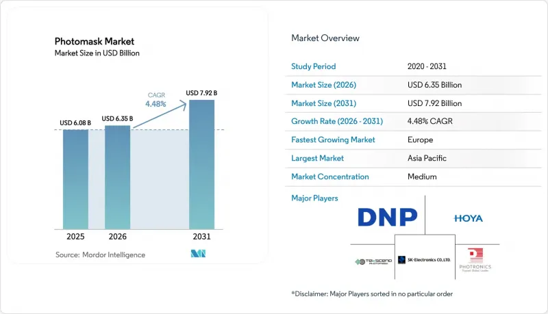
포토마스크 시장 규모는 2025년에 60억 8,000만 달러로 평가되었고 2026년 63억 5,000만 달러에서 2031년까지 79억 2,000만 달러에 이를 것으로 예측되며, 예측 기간(2026-2031년) CAGR은 4.48%를 나타낼 전망입니다.
고해상도 레티클, 보다 엄격한 CD(Critical Dimension) 관리, 결함 없는 마스크 블랭크에 대한 지속적인 수요가 이러한 꾸준한 성장을 뒷받침하고 있습니다. 대만과 한국의 고NA EUV 장비 도입이 가속화되면서 평균 판매가격이 상승하고 있습니다. 이는 리소그래피 노드가 진화할수록 더 진보된 위상변환 기술과 흡수재가 필요하기 때문입니다. 또한, 포토마스크 시장은 반도체 공급망 현지화를 위한 전 세계적인 움직임의 수혜를 받고 있습니다. 미국과 유럽연합(EU)의 신규 팹은 자본 효율성을 최적화하기 위해 자체 생산이 아닌 시판 마스크에 아웃소싱을 선택하고 있습니다. 한편, 칩렛 기반 설계는 재배선층(RDL) 및 인터포저용 마스크에 대한 수요를 점차 증가시키고 있으며, 포토마스크의 소비는 프론트엔드 웨이퍼 가공에서 첨단 패키징 분야로 확대되고 있습니다. 8세대 이상의 AMOLED 라인으로 전환을 추진하고 있는 디스플레이 패널 업체들도 성장의 요인으로 작용하고 있습니다. 새로운 라인마다 최대 30개의 고유한 디스플레이 마스크가 소비되기 때문에 레이어 수가 증가하여 팹당 수익이 증가하기 때문입니다.
세계 포토마스크 시장 동향과 인사이트
대만 및 한국에서의 고NA EUV 리소그래피 도입
고NA EUV 장비의 적극적인 도입은 업계가 옹스트롬 시대로 진입했음을 의미하며, 마스크 제조업체는 10nm 이하의 패턴 정확도와 인쇄 가능한 결함을 거의 제로에 가깝게 억제할 것을 요구하고 있습니다. TSMC와 삼성은 현재 기존 EUV 세트에 비해 고NA 마스크 1장당 3-4배의 가격을 지불하고 있으며, 생산량이 정체되어 있음에도 불구하고 공급업체의 수익이 확대되고 있습니다. 한국이 수립한 4,710억 달러 규모의 반도체 클러스터 계획에는 자체 포토마스크 인프라 구축이 포함되어 있으며, 이를 통해 수입 의존도를 낮추고 지역 내 물류 체계를 재구축할 수 있을 것으로 기대됩니다. 중국의 세컨드 티어 파운더리도 수출규제 장벽이 완화되면, 늦어지기는 하겠지만 필연적으로 이에 따라 도입을 추진할 것으로 예측됩니다. 이러한 추세는 종합적으로 첨단과 기존 포토마스크 생산의 기술 격차를 확대하여 기존 포토마스크 생산의 수익률을 낮추는 동시에 고급 제품의 수익성을 높일 수 있습니다.
미국-EU의 CHIPS법, 시판용 마스크의 아웃소싱 촉진
미국의 527억 달러 규모의 국내 인센티브 프로그램과 유럽에서도 이에 상응하는 조치가 시행되고 있으며, 규모가 너무 작은 신규 마스크 생산업체들이 자체 마스크 생산 시설을 건설하도록 장려하고 있습니다. 이에 대해 시판용 마스크 공급업체들은 애리조나, 오하이오, 드레스덴에 위치한 첨단 팹 옆에 클린룸을 설치하여 사이클 타임을 단축하고 지정학적 위험에 대한 내성을 높이고 있습니다. 이러한 지역 분산화 움직임은 아시아태평양에 대한 과도한 의존도를 줄이는 것으로, 긴장이 고조되고 있는 상황에서 전략적 필수 사항입니다. 초기 아웃소싱 계약에는 3nm 및 2nm 노드 전용 툴 세트가 규정되어 있어 장기적인 수익원을 확보할 수 있습니다. 시간이 지남에 따라 자본을 절약하기 위해 단일 거점의 자체 마스크 공장을 폐쇄하는 사례가 증가함에 따라 외부 공급업체는 협상력을 높이고 있습니다.
EUV 마스크 블랭크의 결함 밀도가 5 결함/cm2를 초과하면 스크랩이 증가합니다.
결함 밀도가 5 결함/cm2의 임계치를 초과하면 팹은 EUV 마스크 블랭크의 최대 25%를 폐기해야 하며, 이는 장당 5만-10만 달러의 비용 증가와 테이프 아웃 일정의 지연을 초래합니다. 인증된 공급업체는 한정되어 있으며(주로 AGC와 신에츠화학공업), 보다 엄격한 사양을 충족시키면서 생산량을 확대하는 데 어려움을 겪고 있습니다. 새로운 검사 광학 및 세척 레시피로 인해 입자 수가 감소하고 있지만, 2 결함/cm2 미만을 달성하는 길은 여전히 불투명합니다. 지속적인 폐기처분은 공급업체의 수익률을 압박하고, 2025-2026년으로 예정된 팹 양산에 부담을 주고 있습니다. 공급 부족이 장기화되면 고급 마스크의 납품이 정체되어 포토마스크 시장의 CAGR이 둔화될 수 있습니다.
부문 분석
2025년 매출의 대부분은 레티클이 차지해, 포토마스크 시장의 65.90%를 차지했습니다. 이는 10nm 이하의 모든 중요 레이어에서 라인 엣지의 거칠기를 사양 범위 내에서 유지하기 위해 완벽한 이미지 전사가 필요하기 때문입니다. 높은 가격 설정은 고도의 레지스트 상호 작용 및 위상 시프트 조정을 보완할 필요성에 기인합니다. 고NA EUV가 발전함에 따라 각 소자층마다 맞춤형 조명이 요구되는 경우가 많아 웨이퍼 한 장당 마스크 사용량이 증가하고 있습니다. 마스터 마스크는 4.99%의 연평균 복합 성장률(CAGR)로 가장 빠르게 성장하고 있습니다. 이는 멀티패터닝 공정에서 스텝 앤 리피트 방식의 도터 마스크 제조에 공급할 고충실도 템플릿이 필요하기 때문입니다. 카피 마스크와 도터 마스크는 여전히 레거시 노드에 대응하고 있지만, 고급 노드가 주류가 되면서 그 수량 성장이 둔화되고 있습니다. 전체적으로 레티클 및 마스터 마스크의 포토마스크 시장 규모는 2031년까지 웨이퍼 시작 수와 연동하여 확대될 것으로 예측됩니다.
DNP의 2nm 이하 공정용 EUV 마스크의 성공적인 시연은 제품 혁신이 어떻게 경쟁 우위를 확보할 수 있는지를 잘 보여줍니다. 현재 레티클 공급업체들은 AI 기반 결함 예측을 통합하여 리핀율을 낮추고 팹의 사이클 타임을 개선하고 있습니다. 대만이나 한국에 집중된 양산 거점에서는 팹 근처에 재고를 앞당겨 당일 배송이 가능한 벤더를 우대하기 때문에 지역 위성 거점에 대한 투자가 촉진되고 있습니다. 전환 비용이 높기 때문에 기술 인증을 획득하면 고객 충성도가 견고하게 유지되고, 공정 세대에 걸친 수익 전망을 확보할 수 있습니다.
바이너리 크롬 마스크는 65nm 및 그 이전 노드뿐만 아니라 대부분의 디스플레이 층을 지원하는 비용 효율적인 제조 공정 덕분에 2025년 포토마스크 시장에서 가장 큰 43.90%의 점유율을 차지했습니다. 그 지속적인 중요성은 시장 침체기에도 공급업체들의 현금 흐름을 지탱해주고 있습니다. 한편, EUV 마스크는 파운드리 및 IDM의 3nm 이하 공정 확대에 힘입어 5.29%의 가장 높은 CAGR을 기록했습니다. 각 EUV 마스크는 광학 크롬 마스크 가격의 배수로 판매되기 때문에 판매 수량은 적지만 매출은 확대됩니다. 감쇠형 및 교대 위상 시프트 마스크는 중요한 레이어에서 광학 흐름을 보완하고, 나노 임프린트 템플릿은 피처의 균일성이 임프린트 편차를 허용할 수 있는 경우 고처리량 및 저비용의 대안을 제공함으로써 메모리 패터닝에서 틈새 시장을 형성하고 있습니다.
메모리 제조업체들이 특정 레이어를 EUV로 전환하고 새로운 리소그래피 기술 도입 없이 고밀도화를 추구함에 따라 EUV 제품의 포토마스크 시장 규모는 확대될 것으로 예측됩니다. 캐논의 나노임프린트 로드맵은 특정 응용 분야에서 대안을 제시함으로써 EUV 가격 하락 압력을 계속 가하고 있지만, EUV는 다양한 패턴 형상에 대해 더 높은 유연성과 처리량을 유지하고 있습니다. 각 공급업체들은 크롬 마스크 생산능력을 유지하면서 EUV에 필요한 멀티빔 라이터와 페리클 라인에 설비투자를 집중함으로써 포트폴리오의 균형을 맞추고 있습니다.
지역별 분석
2025년에는 아시아태평양이 전 세계 매출의 71.10%를 차지했습니다. 이는 대만, 한국, 중국에 최첨단 팹이 가장 밀집되어 있고, 마스크 제조 생태계가 가장 잘 갖추어져 있기 때문입니다. TSMC는 전 세계 파운드리 매출의 60% 이상을 차지하고 있으며, 매 분기마다 막대한 레티클 수요를 창출하고 있습니다. 신에츠화학공업의 석영 기판, NuFlare의 멀티빔 라이터, Mycronic의 수리 도구 등 상호 보완적인 공급망을 통해 동일 지역 내 조달이 가능하여 사이클 타임의 리스크를 최소화하고 있습니다. 중국은 수출 규제에도 불구하고 두 자릿수 속도로 성숙한 노드의 생산 능력을 지속적으로 증가시켜 광학 크롬 마스크에 대한 지속적인 수요를 보장하고 있습니다. 한국의 4,710억 달러 규모의 클러스터 계획은 2047년까지 16개의 신규 팹이 건설되고, 각각 전용 포토마스크 인프라가 구축되어 아태지역에서의 우위를 더욱 강화할 것입니다.
유럽은 유럽 반도체법(European Chips Act)에 따라 정부가 반도체 자급자족 프로그램에 자금을 지원함에 따라 연평균 4.55%로 가장 빠르게 성장하고 있습니다. 드레스덴에 설치된 Tekscend Photomask의 멀티빔 장비는 복잡한 마스크의 노출 시간을 며칠에서 단 몇 시간으로 단축하여 유럽 대륙이 첨단 노드 생산에 대한 준비가 되어 있음을 보여줍니다. 독일은 ZEISS SMT가 예나, 오버코헨, 베츨러에서 마스크 솔루션 거점을 확장하고 광학, 블랭크, 노광 공정을 현지 팹의 니즈에 맞게 조정함으로써 이 지역의 중심적인 역할을 담당하고 있습니다. 전략적 초점은 자동차 및 산업용 칩에 있으며, 유럽은 이미 설계 및 시스템 전문 지식을 보유하고 있으며, 국내 포토마스크 채택을 확대되고 있습니다.
북미에서는 527억 달러 규모의 'CHIPS법'에 따른 인센티브가 활용되어 애리조나주, 오하이오주, 뉴욕주에서 팹 프로젝트가 추진되고 있습니다. 이로 인해 인근의 마스크 공급업체에 대한 새로운 수요가 발생하고 있습니다. TSMC가 애리조나주에 건설하는 1,650억 달러 규모의 단지만 해도 연간 수천 장의 EUV 마스크를 소비할 것으로 예상되며, 아시아 및 유럽 공급업체들이 현지에 위성 공장을 설립할 것을 촉구하고 있습니다. 인텔의 파운드리 사업에 대한 집중, 세계 파운드리의 확장, 그리고 여러 전문 팹이 결합되어 고객 기반이 다양화되고 있습니다. 그러나 비용 구조는 여전히 아시아태평양보다 높기 때문에 수익률은 단납기 시제품 제작 및 현장 결함 분석과 같은 부가가치 서비스에 의존하고 있습니다.
기타 특전:
- 엑셀 형식 시장 예측(ME) 시트
- 3개월간 애널리스트 지원
자주 묻는 질문
목차
제1장 서론
제2장 조사 방법
제3장 주요 요약
제4장 시장 구도
제5장 시장 규모와 성장 예측
제6장 경쟁 구도
제7장 시장 기회와 향후 전망
JHS 26.05.20The photomask market size was valued at USD 6.08 billion in 2025 and estimated to grow from USD 6.35 billion in 2026 to reach USD 7.92 billion by 2031, at a CAGR of 4.48% during the forecast period (2026-2031).

Sustained demand for higher-resolution reticles, tighter critical-dimension control and defect-free mask blanks underpins this steady growth. Accelerated deployment of High-NA EUV tools in Taiwan and Korea is lifting average selling prices because every successive lithography node requires more sophisticated phase-shift engineering and absorber materials. The photomask market also benefits from the global push to localize semiconductor supply chains; new fabs in the United States and the European Union are choosing merchant mask outsourcing over in-house shops to optimize capital efficiency. Meanwhile, chiplet-based designs spur incremental demand for redistribution-layer (RDL) and interposer masks, spreading photomask consumption beyond front-end wafer processing into advanced packaging. Display panel makers moving to Gen 8+ AMOLED lines add another vector of growth because each new line consumes up to 30 unique display masks, elevating layer counts and revenue per fab.
Global Photomask Market Trends and Insights
High-NA EUV lithography adoption in Taiwan and Korea
Aggressive rollout of High-NA EUV tools marks the industry's transition into the angstrom era, forcing mask makers to deliver sub-10 nm pattern fidelity with near-zero printable defects. TSMC and Samsung now pay three to four times more per High-NA mask than for conventional EUV sets, expanding supplier revenue even as unit volumes stay stable. Korea's USD 471 billion semiconductor cluster plan includes captive photomask infrastructure, lowering import reliance and reshaping regional logistics. Tier-two foundries in China are expected to follow with delayed but inevitable adoption once export-control barriers ease. These developments collectively widen the technology gap between leading-edge and legacy photomask production, pushing legacy margins downward while boosting high-end profitability.
U.S./EU CHIPS Acts fueling merchant mask outsourcing
Domestic incentive programs worth USD 52.7 billion in the United States and comparable measures in Europe encourage new fabs that lack scale to build proprietary mask shops. Merchant suppliers are responding by colocating cleanrooms next to advanced fabs in Arizona, Ohio, and Dresden, improving cycle-times and geopolitical resilience. The regionalization thrust reduces over-dependence on Asia-Pacific sources, a strategic imperative amid rising tensions. Early outsourcing contracts stipulate dedicated toolsets for 3 nm and 2 nm nodes, locking in long-term revenue streams. Over time, merchant providers gain bargaining power as more single-site captive shops shutter to conserve capital.
EUV mask-blank defectivity above 5 defects/cm2 escalating scrap
Defect densities beyond the 5 defects/cm2 threshold force fabs to scrap up to 25% of EUV mask blanks, inflating costs by USD 50,000-100,000 each and delaying tape-out schedules. Limited qualified suppliers-mainly AGC and Shin-Etsu-struggle to scale volumes while meeting tighter specifications. Although new inspection optics and cleaning recipes lower particle counts, the road to sub-2 defects/cm2 remains uncertain. Persistent scrap erodes supplier margins and strains fab ramp-ups slated for 2025-2026. Any prolonged shortage could stall high-end mask deliveries and temper the photomask market CAGR.
Other drivers and restraints analyzed in the detailed report include:
- AMOLED Gen 8+ fabs driving 30-layer display masks
- Chiplet RDL and interposer photomasks upsurge
- Japan quartz-substrate supply bottlenecks
For complete list of drivers and restraints, kindly check the Table Of Contents.
Segment Analysis
Reticles generated the bulk of 2025 revenue, holding 65.90% of the photomask market, because every critical layer at sub-10 nm requires flawless image transfer to maintain line-edge roughness within spec. Premium pricing stems from the need to offset sophisticated resist interactions and phase-shift tuning. As High-NA EUV progresses, each device layer often demands bespoke illumination, expanding mask counts per wafer start. Master masks are growing fastest at a 4.99% CAGR because multi-patterning flows require high-fidelity templates that feed step-and-repeat daughter mask production. Copy and daughter masks still address legacy nodes but show subdued volume growth as advanced nodes take center stage. Collectively, the photomask market size for reticles and masters is expected to rise in tandem with wafer starts through 2031.
DNP's successful demonstration of EUV masks for beyond-2 nm processes underscores how product innovation secures competitive advantage. Reticle suppliers now integrate AI-based defect prediction to lower re-spin rates, improving fab cycle time. Volume manufacturing clusters in Taiwan and Korea favor vendors that can preload inventory near fabs for same-day deliveries, prompting investment in regional satellite sites. Given the high switching costs, customer loyalty remains strong once technical qualification is achieved, preserving revenue visibility across process generations.
Binary chrome masks held the largest 43.90% slice of the photomask market in 2025 thanks to cost-efficient manufacturing that continues to serve 65 nm and older nodes plus most display layers. Their enduring relevance anchors supplier cash flows during market lulls. EUV masks, however, carry the fastest 5.29% CAGR, fueled by sub-3 nm process ramps at foundries and IDMs. Each EUV mask sells at a multiple of optical chrome pricing, magnifying revenue despite lower unit volume. Attenuated and alternating phase-shift masks complement optical flows for critical layers, while nano-imprint templates establish a niche in memory patterning by offering high-throughput, low-cost alternatives when feature uniformity tolerates imprint variability.
The photomask market size for EUV products should expand as memory makers migrate select layers to EUV, adding density without new lithography options. Canon's nano-imprint roadmap keeps downward pressure on EUV pricing by signaling a substitute for specific applications, but EUV retains higher flexibility and throughput for diverse pattern geometries. Suppliers balance portfolios by keeping chrome capacity viable while funneling capital expenditures toward multibeam writers and pellicle lines required for EUV.
The Photomask Market Report is Segmented by Product Type (Reticle, Master Mask, and Copy/Daughter Mask), Mask Type (Binary Chrome Mask, Attenuated Phase Shift Mask, Alternating Phase Shift Mask, and More), Application (Semiconductor and IC Manufacturing, Flat-Panel Displays, and More), End-Use Industry (Foundries and IDMs, Fabless Design Houses, and More), and Geography. The Market Forecasts are Provided in Terms of Value (USD).
Geography Analysis
Asia-Pacific secured 71.10% of global sales in 2025 because Taiwan, Korea and China host the densest concentration of cutting-edge fabs and the most complete mask-making ecosystem. TSMC alone represents more than 60% of global foundry revenue, commanding massive reticle volumes each quarter. Complementary supply chains-quartz substrates from Shin-Etsu Chemical, multibeam writers from NuFlare and repair tools from Mycronic-enable same-region procurement, minimizing cycle-time risk. China continues adding mature-node capacity at a double-digit clip despite export constraints, ensuring ongoing demand for optical chrome masks. Korea's USD 471 billion cluster plan adds 16 new fabs through 2047, each with dedicated photomask infrastructure, reinforcing Asia-Pacific pre-eminence.
Europe is growing fastest at 4.55% CAGR as governments fund semiconductor sovereignty programs under the European Chips Act. Tekscend Photomask's multibeam installation in Dresden cuts writing time for complex masks from days to mere hours, signaling continental readiness for advanced-node production. Germany anchors the region through ZEISS SMT's expansion of mask-solutions sites in Jena, Oberkochen and Wetzlar, aligning optics, blanks and writing to local fab needs. Strategic focus rests on automotive and industrial chips, where Europe already wields design and systems expertise, augmenting domestic photomask uptake.
North America benefits from USD 52.7 billion in CHIPS Act incentives that spur fab projects in Arizona, Ohio and New York, creating fresh demand for proximate mask suppliers. TSMC's USD 165 billion Arizona complex alone will consume thousands of EUV masks annually, inviting both Asian and European vendors to establish local satellite operations. Intel's foundry push, GlobalFoundries' expansions and multiple specialty fabs together diversify the customer base. However, cost structures remain higher than in Asia-Pacific, so profit margins depend on value-added services such as rapid-turn prototypes and on-site defect analysis.
- Tekscend Photomask Inc. (Toppan)
- Dai Nippon Printing Co., Ltd.
- Photronics, Inc.
- Hoya Corporation
- SK-Electronics Co., Ltd.
- Nippon Filcon Co., Ltd.
- Compugraphics International Ltd.
- Taiwan Mask Corporation
- Mycronic AB
- LG Innotek Co., Ltd.
- Advanced Mask Technology Center GmbH
- Shenzhen Qingyi Photomask Ltd.
- NuFlare Technology Inc.
- Canon Inc.
- IMS Nanofabrication GmbH
- Applied Materials, Inc.
- ASML Holding N.V.
- Fujifilm Holdings Corp.
- Advantest Corp.
- Vistec Electron Beam
- JENOPTIK AG
Additional Benefits:
- The market estimate (ME) sheet in Excel format
- 3 months of analyst support
TABLE OF CONTENTS
1 INTRODUCTION
- 1.1 Study Assumptions and Market Definition
- 1.2 Scope of the Study
2 RESEARCH METHODOLOGY
3 EXECUTIVE SUMMARY
4 MARKET LANDSCAPE
- 4.1 Market Overview
- 4.2 Market Drivers
- 4.2.1 High-NA EUV Lithography Adoption in Taiwan and Korea
- 4.2.2 U.S./EU CHIPS Acts Fueling Merchant Mask Outsourcing
- 4.2.3 AMOLED Gen 8+ Fabs Driving 30-Layer Display Masks
- 4.2.4 ADAS and Power-SemiLess than 28 nm Demand for Large-Area Reticles
- 4.2.5 Chiplet RDL and Interposer Photomasks Upsurge
- 4.2.6 AI-Enabled Defect Inspection Cutting TAT for Captive Shops
- 4.3 Market Restraints
- 4.3.1 EUV Mask-Blank Defectivity Above 5 defects/cm2 Escalating Scrap
- 4.3.2 Japan Quartz-Substrate Supply Bottlenecks
- 4.3.3 Export Controls on Multi-Beam Writers Limiting China
- 4.3.4 Rising Electricity Tariffs in Korea and Taiwan
- 4.4 Industry Ecosystem Analysis
- 4.5 Technological Outlook
- 4.6 Porter's Five Forces Analysis
- 4.6.1 Bargaining Power of Suppliers
- 4.6.2 Bargaining Power of Buyers
- 4.6.3 Threat of New Entrants
- 4.6.4 Threat of Substitutes
- 4.6.5 Competitive Rivalry
5 MARKET SIZE AND GROWTH FORECASTS (VALUES)
- 5.1 By Product Type
- 5.1.1 Reticle (4X/5X)
- 5.1.2 Master Mask
- 5.1.3 Copy/Daughter Mask
- 5.2 By Mask Type
- 5.2.1 Binary Chrome Mask (BCM)
- 5.2.2 Attenuated Phase Shift Mask (Att-PSM)
- 5.2.3 Alternating Phase Shift Mask (Alt-PSM)
- 5.2.4 Chromeless Phase Lithography Mask
- 5.2.5 EUV Photomask
- 5.2.6 Nano-imprint Template
- 5.3 By Application
- 5.3.1 Semiconductor and IC Manufacturing
- 5.3.1.1 More than 65 nm
- 5.3.1.2 45-28 nm
- 5.3.1.3 22-14 nm
- 5.3.1.4 10-7 nm
- 5.3.1.5 5 nm
- 5.3.1.6 Upto 3 nm
- 5.3.2 Flat-Panel Displays
- 5.3.2.1 LCD
- 5.3.2.2 AMOLED
- 5.3.2.3 OLED Micro-display
- 5.3.3 MEMS Sensors
- 5.3.4 Advanced Packaging (RDL/Interposer)
- 5.3.5 Photonics and Silicon Photonics
- 5.3.6 Others
- 5.3.1 Semiconductor and IC Manufacturing
- 5.4 By End-use Industry
- 5.4.1 Foundries and IDMs
- 5.4.2 Fabless Design Houses
- 5.4.3 Display Panel Manufacturers
- 5.4.4 OSAT/Advanced Packaging Providers
- 5.4.5 Research and Academia
- 5.4.6 Aerospace and Defense
- 5.4.7 Telecommunications OEMs
- 5.5 By Geography
- 5.5.1 North America
- 5.5.1.1 United States
- 5.5.1.2 Canada
- 5.5.1.3 Mexico
- 5.5.2 Europe
- 5.5.2.1 Germany
- 5.5.2.2 United Kingdom
- 5.5.2.3 France
- 5.5.2.4 Nordics
- 5.5.2.5 Rest of Europe
- 5.5.3 South America
- 5.5.3.1 Brazil
- 5.5.3.2 Rest of South America
- 5.5.4 Asia-Pacific
- 5.5.4.1 China
- 5.5.4.2 Japan
- 5.5.4.3 India
- 5.5.4.4 South-East Asia
- 5.5.4.5 Rest of Asia-Pacific
- 5.5.5 Middle East and Africa
- 5.5.5.1 Middle East
- 5.5.5.1.1 Gulf Cooperation Council Countries
- 5.5.5.1.2 Turkey
- 5.5.5.1.3 Rest of Middle East
- 5.5.5.2 Africa
- 5.5.5.2.1 South Africa
- 5.5.5.2.2 Rest of Africa
- 5.5.5.1 Middle East
- 5.5.1 North America
6 COMPETITIVE LANDSCAPE
- 6.1 Market Concentration
- 6.2 Strategic Moves
- 6.3 Market Share Analysis
- 6.4 Company Profiles {(includes Global level Overview, Market level overview, Core Segments, Financials as available, Strategic Information, Market Rank/Share for key companies, Products and Services, and Recent Developments)}
- 6.4.1 Tekscend Photomask Inc. (Toppan)
- 6.4.2 Dai Nippon Printing Co., Ltd.
- 6.4.3 Photronics, Inc.
- 6.4.4 Hoya Corporation
- 6.4.5 SK-Electronics Co., Ltd.
- 6.4.6 Nippon Filcon Co., Ltd.
- 6.4.7 Compugraphics International Ltd.
- 6.4.8 Taiwan Mask Corporation
- 6.4.9 Mycronic AB
- 6.4.10 LG Innotek Co., Ltd.
- 6.4.11 Advanced Mask Technology Center GmbH
- 6.4.12 Shenzhen Qingyi Photomask Ltd.
- 6.4.13 NuFlare Technology Inc.
- 6.4.14 Canon Inc.
- 6.4.15 IMS Nanofabrication GmbH
- 6.4.16 Applied Materials, Inc.
- 6.4.17 ASML Holding N.V.
- 6.4.18 Fujifilm Holdings Corp.
- 6.4.19 Advantest Corp.
- 6.4.20 Vistec Electron Beam
- 6.4.21 JENOPTIK AG
7 MARKET OPPORTUNITIES AND FUTURE OUTLOOK
- 7.1 White-space and Unmet-Need Assessment
