
|
시장보고서
상품코드
2035033
반도체 리드프레임 시장 : 점유율 분석, 업계 동향 및 통계, 성장 예측(2026-2031년)Semiconductor Lead Frame - Market Share Analysis, Industry Trends & Statistics, Growth Forecasts (2026 - 2031) |
||||||
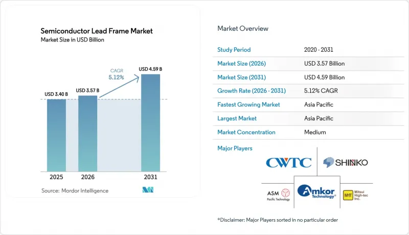
반도체 리드프레임 시장 규모는 2025년에 34억 달러로 평가되었고 2026년 35억 7,000만 달러에서 2031년까지 45억 9,000만 달러에 이를 것으로 예측되며, 예측 기간(2026-2031년) CAGR은 5.12%를 나타낼 전망입니다.
자동차 전장, 5G 인프라, AI 탑재 엣지 디바이스에서 고속 신호에 대응하면서도 효과적으로 열을 방출할 수 있는 컴팩트한 패키지가 요구되면서 수요가 가속화되고 있습니다. 소형화의 진전에 따라 생산량은 쿼드 플랫 노 리드(QFN) 및 듀얼 플랫 노 리드(DFN) 변형으로 전환되고, 전기자동차(EV)의 파워일렉트로닉스 채용 확대에 따라 더 높은 열 부하를 견딜 수 있는 구리 기반 프레임에 대한 사양이 높아졌습니다. CHIPS 법에 따라 북미와 유럽에 새로운 생산능력이 창출되었고, 아시아태평양의 기존 생산기지와 함께 공급망의 지역적 분산이 가속화되었습니다. 동시에 구리와 은의 가격 변동에 대응하고 실리콘 카바이드(SiC)와 질화갈륨(GaN) 기술을 지원하기 위한 재료 혁신으로 복합재료와 다층 구조가 대중화되었습니다.
세계 반도체 리드프레임 시장 동향과 인사이트
소비자 전자기기 수요 급증
2024년과 2025년 초에 스마트폰, 웨어러블, 게임기 출하량이 급증하면서 제품 개발 주기가 단축되고, 설계자들은 설치 면적을 늘리지 않고도 방열 경로를 개선할 수 있는 더 얇은 QFN 아웃라인을 채택하고 있습니다. 전 세계 생산량의 약 4분의 1은 이미 0.1mm 미만의 리드프레임 두께를 채택하고 있으며, 이를 통해 하이엔드 휴대폰 내부 부품의 고밀도화가 가능해졌습니다. 여러 OSAT 공급업체들이 자동차 인증 흐름을 민수용 라인으로 확대하여, 잦은 온도 변동에 노출되는 휴대용 제품에서 0등급 신뢰성을 촉진하고 있습니다. 디바이스 제조업체들이 배터리 수명, 무게, 성능 요구사항의 균형을 맞추면서 이러한 변화가 반도체 리드프레임 시장을 뒷받침했습니다.
EV 및 xEV용 파워 일렉트로닉스의 빠른 성장세
전기자동차(EV) 생산량이 급증하고, 트랙션 인버터는 400V에서 800V 아키텍처로 전환되었습니다. 따라서 리드프레임에는 열전도율과 피로 강도가 향상된 구리 합금이 요구되고 있습니다. ROHM의 TRCDRIVE pack(TM) SiC 모듈은 최대 300kW까지 낮은 스위칭 손실을 유지하기 위해 최적화된 열 확산이 필요하다는 것을 보여주었습니다. Tier 1 공급업체는 차량의 장기적인 서비스 수명 동안 부식을 억제하기 위해 프레스 가공된 구리와 니켈-팔라듐 도금 마감을 결합한 복합 프레임을 지정했습니다. 자동차 업계의 조달 수요 증가는 반도체 리드프레임 시장에서의 수익 전망을 넓히고 장기적인 수주를 확고히 했습니다.
설비투자 집중과 생산 병목현상
파인피치 대응 턴키 프레스 라인은 사이트당 3억 달러를 넘어섰고, 다이패드의 미세화에 따라 금형 비용도 상승했습니다. 중소 벤더들은 자금 압박에 직면해 일부 업체는 대형 OSAT와의 합병이나 생산 능력의 라이선싱에 나서기도 했습니다. 95%의 정확도를 자랑하는 AI 탑재 결함 검사 네트워크를 포함한 고도의 자동화는 인력 부족을 일부 보완했지만, 양산 시작까지의 기간을 연장시켰습니다. 생산 능력의 압박으로 인해 고객 인증이 지연될 수 있으며, 이는 반도체 리드프레임 시장의 역풍으로 작용하고 있습니다.
부문 분석
QFN 패키지는 2025년 출하량의 31.65%를 차지했으며, 기판 면적이 제한된 환경에서 열효율 측면에서 여전히 최적의 선택으로 자리매김하고 있습니다. 리드 피치 및 센터 패드의 미세화를 향한 이 부문의 진화는 자동차 센서 및 프리미엄 스마트폰의 신뢰성을 향상시켰습니다. 2031년까지 연평균 복합 성장률(CAGR) 8.45%로 예상되는 DFN 패키지는 웨어러블 기기 및 소형 IoT 엔드노드에 적합한 더 얇은 프로파일을 제공했습니다. QFN과 DFN이 결합하여 견고한 수익원을 유지하며 반도체 리드프레임 시장의 상승 추세를 뒷받침했습니다.
드롭인 히트 슬러그, 더블 다이 스태킹과 같은 기술의 발전으로 QFP의 이용 사례는 더욱 확대되었습니다. 반면, DIP 및 SOP 패키지는 소형화보다 비용이 중시되는 레거시 시장과 산업용 시장으로 점차 이동하고 있습니다. 플립칩의 윤곽은 고성능 컴퓨팅을 지원하지만, 노출된 리드 대신 도금된 구리 기둥이 필요했습니다. 이 카테고리 전체에서 QFN 및 DFN 반도체 리드프레임 시장 규모는 지속적인 스마트폰 모델 교체 주기와 차량용 모듈의 경량화를 요구하는 규제 추진으로 인해 전체 산업 성장률을 상회할 것으로 예측됐습니다.
스탬핑은 시간당 9만 스트로크 이상의 고속 프레스와 모듈식 다이세트 덕분에 2025년 생산량의 62.75%를 유지했습니다. 연속 스트립 도금은 귀금속 사용량을 제한하는 선택적 마감을 실현했습니다. 그러나 설계자들이 열 확산을 위해 구리 코어에 몰리브덴과 알루미늄을 내장하고 있기 때문에 다층 복합재는 2031년까지 연평균 복합 성장률(CAGR) 9.05%를 나타낼 것으로 예측됩니다. 이러한 프리미엄 구성은 EV 인버터의 가혹한 사용 조건에 대한 반도체 리드프레임 시장의 대응을 반영합니다.
에칭 기술은 5G 빔포머 및 광모듈용 소량, 고정밀 회로에서 점유율을 확보했습니다. 레이저 보조 포토레지스트 노광으로 엣지 선명도가 향상되어 ±5µm의 치수 제어가 가능해졌습니다. 반도체 리드프레임 업계는 복잡성이 증가함에 따라 미세구조는 에칭을, 기계적 견고성은 스탬핑을 채택하는 하이브리드 플로우로 연구개발을 할당하여 제품 출시 기간 단축이라는 어려운 상황에서 비용과 성능의 균형을 맞추기 위해 노력하고 있습니다.
반도체 리드프레임 시장은 패키지 유형(DIP(듀얼 인 라인 패키지, SOP(Small Outline Package) 등), 제조 공정(스탬핑 리드프레임, 에칭 리드프레임 등), 용도(집적회로, 개별 디바이스 등), 산업 분야(가전, 자동차 등), 지역(북미, 유럽, 아시아태평양, 중동 및 아프리카 등)으로 분류됩니다. 등), 산업 분야(가전, 자동차 등), 그리고 지역(북미, 남미, 유럽, 아시아태평양, 중동 및 아프리카)으로 구분됩니다.
지역별 분석
아시아태평양은 2025년 세계 매출의 41.10%를 차지했으며, 2031년까지 연평균 복합 성장률(CAGR) 8.75%를 나타낼 것으로 전망됩니다. 중국에서는 420억 개 이상의 스탬핑 리드프레임이 출하된 반면, 일본의 정밀 에칭 전문 기업은 운전 지원 시스템용 고주파 모듈을 공급했습니다. 베트남과 말레이시아에서는 3억 달러 이상의 투자로 SiC 파워 하이브리드에 대응하기 위해 도금 라인을 업데이트했습니다.
북미에서는 'CHIPS법'으로 인해 새로운 동력이 생겼습니다. 이 법은 제조기지 확장에 390억 달러, 연구개발(R&:D)에 132억 달러를 배정했습니다. 팹(제조공장)의 생산능력은 2032년까지 203% 증가할 것으로 예상되며, 이질적 통합 로드맵에 부합하는 국내 조달 프레임에 대한 수요를 창출했습니다. 인텔의 EMIB 및 Foveros 프로그램에서는 독자적인 구리 합금 구성이 필요했고, 공급업체를 차별화할 수 있는 부가가치 계층이 필요했습니다.
유럽은 2030년까지 세계 반도체 생산량의 20%를 목표로 하는 430억 유로(499억 달러) 규모의 '유럽 칩법'에 힘입어 고신뢰성 자동차 및 산업용도에 집중하고 있습니다. 현지의 IC 기판 생산 능력이 제한적이기 때문에 독일 자동차 제조업체 근처에 복합재 및 에칭 프레임 생산라인을 구축할 준비가 된 신규 진출기업에게 진입할 수 있는 여지가 남아있었습니다. 원자재 가격 상승(구리 9%, 알루미늄 8% 상승)으로 인해 유럽 기업들은 탄소 감축 의무에 따라 재활용 방안을 모색하고, 반도체 리드프레임 산업공급망 복원력을 강화했습니다.
기타 특전:
- 엑셀 형식 시장 예측(ME) 시트
- 3개월간 애널리스트 지원
자주 묻는 질문
목차
제1장 서론
제2장 조사 방법
제3장 주요 요약
제4장 시장 구도
제5장 시장 규모와 성장 예측
제6장 경쟁 구도
제7장 시장 기회와 향후 전망
JHS 26.05.20The semiconductor lead frame market size was valued at USD 3.40 billion in 2025 and estimated to grow from USD 3.57 billion in 2026 to reach USD 4.59 billion by 2031, at a CAGR of 5.12% during the forecast period (2026-2031).

Demand accelerated as automotive electronics, 5G infrastructure, and AI-enabled edge devices required compact packages that dissipate heat effectively while supporting high-speed signals. Miniaturization shifted unit volumes toward Quad Flat No-Lead (QFN) and Dual Flat No-Lead (DFN) variants, and power-electronics adoption in electric vehicles (EVs) lifted specifications for copper-based frames able to endure higher thermal loads. Regionalization of supply chains gathered momentum as the CHIPS Act prompted fresh capacity in North America and Europe, complementing entrenched production hubs in Asia-Pacific. At the same time, composite and multi-layer structures gained traction as material innovations aimed to counter copper and silver price volatility and support silicon carbide (SiC) and gallium nitride (GaN) technologies.
Global Semiconductor Lead Frame Market Trends and Insights
Consumer-electronics demand spike
Surging smartphone, wearable, and gaming-device shipments in 2024 and early 2025 tightened product-development cycles and pushed designers toward slimmer QFN outlines that improved thermal paths without enlarging footprints. Roughly one quarter of global output already uses lead-frame thicknesses below 0.1 mm, enabling higher component density inside premium mobiles. Several OSAT providers extended automotive-qualified flows to consumer lines, promoting Grade-0 reliability in handheld products that faced frequent temperature swings. These shifts sustained the semiconductor lead frame market as device makers balanced battery life, weight, and performance requirements.
EV and xEV power-electronics boom
Electric-vehicle production climbed sharply, and traction inverters shifted from 400 V to 800 V architectures. Lead frames, therefore, require copper alloys with improved thermal conductivity and fatigue strength. ROHM's TRCDRIVE pack(TM) SiC module illustrated the need for optimized heat spreading to maintain low switching losses up to 300 kW. Tier-1 suppliers specified composite frames that paired stamped copper with plated nickel-palladium finishes to control corrosion over extended vehicle lifetimes. The automotive procurement wave broadened revenue visibility and anchored long-term orders within the semiconductor lead frame market.
CAPEX intensity and production bottlenecks
Turnkey stamping lines with fine-pitch capability exceeded USD 300 million per site, and tooling costs rose as die pads shrank. Smaller vendors faced liquidity strains, pushing some to merge or license capacity from larger OSATs. High automation levels, including AI-enabled defect-inspection networks with 95% accuracy, partially offset labour shortages but lengthened ramp timelines. Capacity tightness occasionally delays customer qualifications, creating a headwind for the semiconductor lead frame market.
Other drivers and restraints analyzed in the detailed report include:
- 5G/AI edge devices needing QFN/QFP
- Asia-Pacific capacity additions
- Copper and Ag price volatility
For complete list of drivers and restraints, kindly check the Table Of Contents.
Segment Analysis
QFN packages captured 31.65% of 2025 volumes, confirming their role as the preferred choice for thermal efficiency in limited board area. The segment's evolution toward smaller lead pitches and center pads bolstered reliability in automotive sensors and premium smartphones. DFN units, projected to deliver an 8.45% CAGR to 2031, offered even thinner profiles suited to wearables and compact IoT end-nodes. Together, QFN and DFN sustained healthy revenue streams that kept the semiconductor lead frame market on its upward trajectory.
Advances such as drop-in heat slugs and double-die stacking expanded QFP use cases, while DIP and SOP packages gradually migrated to legacy or industrial markets where cost outweighed miniaturization. Flip-chip outlines served high-performance computing but required plated copper pillars rather than exposed leads. Across the category, the semiconductor lead frame market size for QFN and DFN was forecast to outpace wider industry growth, driven by continuous smartphone refresh cycles and regulatory pushes for lighter in-car modules.
Stamping maintained 62.75% of 2025 production thanks to high-speed presses exceeding 90,000 strokes per hour and modular die sets that reduced changeover time. Continuous strip plating added selective finishes that limited precious-metal usage. Multi-layer composites, however, are expected to register a 9.05% CAGR through 2031 as designers combine copper cores with inlaid molybdenum or aluminium for thermal spreading. These premium configurations reflect the semiconductor lead frame market's response to EV inverter stress conditions.
Etching found a share in small-lot, high-precision circuits for 5G beamformers and optical modules. Laser-assisted photoresist exposure improved edge acuity, allowing +-5 µm dimensional control. As complexity rose, the semiconductor lead frame industry allocated research and development toward hybrid flows that used etching for fine features and stamping for mechanical robustness, balancing cost and performance under tightened product-launch windows.
Semiconductor Lead Frame Market is Segmented by Packaging Type (DIP (Dual In-Line Package), SOP (Small Outline Package), and More), Manufacturing Process (Stamping Lead Frame, Etching Lead Frame, and More), Application (Integrated Circuits, Discrete Devices, and More), Industry Vertical (Consumer Electronics, Automotive, and More), and Geography (North America, South America, Europe, Asia-Pacific, and Middle East and Africa).
Geography Analysis
Asia-Pacific held 41.10% of global revenue in 2025 and was expected to log a 8.75% CAGR through 2031. China shipped more than 42 billion stamped frames, while Japan's precision-etch specialists supplied high-frequency modules for driver-assistance systems. Investments exceeding USD 300 million in Vietnam and Malaysia upgraded plating lines to support SiC power hybrids.
North America saw renewed impetus from the CHIPS Act, which earmarked USD 39 billion for fabrication expansion and USD 13.2 billion for R&D. Fab capacity was projected to rise 203% by 2032, creating demand for domestically sourced frames that matched heterogeneous-integration roadmaps. Intel's EMIB and Foveros programs required custom copper-alloy compositions, adding value layers that differentiated suppliers.
Europe concentrated on high-reliability automotive and industrial uses, supported by the Euro 43 billion (USD 49.90 billion) European Chips Act, aiming for 20% global semiconductor output by 2030. Limited local IC-substrate capability left white-space for new entrants ready to establish composite or etched-frame lines near Germany's car manufacturers. Raw-material price escalation-copper up 9% and aluminium up 8%-drove European firms to explore recycling initiatives that aligned with carbon-reduction mandates, reinforcing supply-chain resilience in the semiconductor lead frame industry.
- Mitsubishi Materials Corporation
- Amkor Technology Inc.
- SHINKO ELECTRIC INDUSTRIES CO., LTD.
- Precision Micro Ltd.
- Maxell, Ltd.
- ROHM MECHATECH
- Technic Inc.
- SDI Group, Inc.
- Dai Nippon Printing Co., Ltd.
- Sun Industry Co., Ltd.
- ECE
- Mitsui High-tec, Inc.
- ASM Pacific Technology Ltd.
- Chang Wah Technology Co., Ltd.
- Resonac Corporation
- Jentech Precision Industrial
- Nippon Micro Metal Corp.
- Hitek Fine Metal Co., Ltd.
- SDI Malaysia
- Possehl Electronics
- Jiangsu Hengxin Technology
- Haesung DS Co., Ltd.
- Carsem (M) Sdn Bhd
- Ningbo Kangqiang
Additional Benefits:
- The market estimate (ME) sheet in Excel format
- 3 months of analyst support
TABLE OF CONTENTS
1 INTRODUCTION
- 1.1 Study Assumptions and Market Definition
- 1.2 Scope of the Study
2 RESEARCH METHODOLOGY
3 EXECUTIVE SUMMARY
4 MARKET LANDSCAPE
- 4.1 Market Overview
- 4.2 Market Drivers
- 4.2.1 Consumer-electronics demand spike
- 4.2.2 EV and xEV power-electronics boom
- 4.2.3 5G/AI edge devices needing QFN/QFP
- 4.2.4 Asia-Pacific capacity additions
- 4.2.5 SiC/GaN modules favour Cu lead frames
- 4.2.6 CHIPS-Act-driven on-shore packaging CAPEX
- 4.3 Market Restraints
- 4.3.1 CAPEX intensity and production bottlenecks
- 4.3.2 Copper and Ag price volatility
- 4.3.3 Shift to glass/organic interposers
- 4.3.4 Stricter plating-chemical regulations
- 4.4 Value Chain Analysis
- 4.5 Regulatory Landscape
- 4.6 Technological Outlook
- 4.7 Porter's Five Forces Analysis
- 4.7.1 Threat of New Entrants
- 4.7.2 Bargaining Power of Buyers
- 4.7.3 Bargaining Power of Suppliers
- 4.7.4 Threat of Substitutes
- 4.7.5 Intensity of Competitive Rivalry
- 4.8 Investment Landscape (CAPEX and M&A)
- 4.9 Impact on Macroeconomic factors
5 MARKET SIZE AND GROWTH FORECASTS (VALUE)
- 5.1 By Packaging Type
- 5.1.1 DIP (Dual In-Line Package)
- 5.1.2 SOP (Small Outline Package)
- 5.1.3 SOT (Small Outline Transistor)
- 5.1.4 QFP (Quad Flat Pack)
- 5.1.5 DFN (Dual Flat No-Lead)
- 5.1.6 QFN (Quad Flat No-Lead)
- 5.1.7 FC and TO Packages
- 5.2 By Manufacturing Process
- 5.2.1 Stamping Lead Frame
- 5.2.2 Etching Lead Frame
- 5.2.3 Multi-layer / Composite
- 5.3 By Application
- 5.3.1 Integrated Circuits
- 5.3.2 Discrete Devices
- 5.3.3 Power Modules
- 5.3.4 MEMS and Sensors
- 5.4 By Industry Vertical
- 5.4.1 Consumer Electronics
- 5.4.2 Automotive
- 5.4.3 Industrial and Commercial Electronics
- 5.4.4 Telecommunications
- 5.4.5 Aerospace and Defence
- 5.4.6 Medical Devices
- 5.5 By Geography
- 5.5.1 North America
- 5.5.1.1 United States
- 5.5.1.2 Canada
- 5.5.2 South America
- 5.5.2.1 Brazil
- 5.5.2.2 Argentina
- 5.5.2.3 Rest of South America
- 5.5.3 Europe
- 5.5.3.1 Germany
- 5.5.3.2 United Kingdom
- 5.5.3.3 France
- 5.5.3.4 Italy
- 5.5.3.5 Russia
- 5.5.3.6 Rest of Europe
- 5.5.4 Asia-Pacific
- 5.5.4.1 China
- 5.5.4.2 Japan
- 5.5.4.3 South Korea
- 5.5.4.4 India
- 5.5.4.5 ASEAN
- 5.5.4.6 Rest of Asia-Pacific
- 5.5.5 Middle East and Africa
- 5.5.5.1 Middle East
- 5.5.5.1.1 GCC
- 5.5.5.1.2 Rest of Middle East
- 5.5.5.2 Africa
- 5.5.5.2.1 South Africa
- 5.5.5.2.2 Rest of Africa
- 5.5.5.1 Middle East
- 5.5.1 North America
6 COMPETITIVE LANDSCAPE
- 6.1 Market Concentration
- 6.2 Strategic Moves
- 6.3 Market Share Analysis
- 6.4 Company Profiles (includes Global level Overview, Market level overview, Core Segments, Financials as available, Strategic Information, Market Rank/Share, Products and Services, Recent Developments)
- 6.4.1 Mitsubishi Materials Corporation
- 6.4.2 Amkor Technology Inc.
- 6.4.3 SHINKO ELECTRIC INDUSTRIES CO., LTD.
- 6.4.4 Precision Micro Ltd.
- 6.4.5 Maxell, Ltd.
- 6.4.6 ROHM MECHATECH
- 6.4.7 Technic Inc.
- 6.4.8 SDI Group, Inc.
- 6.4.9 Dai Nippon Printing Co., Ltd.
- 6.4.10 Sun Industry Co., Ltd.
- 6.4.11 ECE
- 6.4.12 Mitsui High-tec, Inc.
- 6.4.13 ASM Pacific Technology Ltd.
- 6.4.14 Chang Wah Technology Co., Ltd.
- 6.4.15 Resonac Corporation
- 6.4.16 Jentech Precision Industrial
- 6.4.17 Nippon Micro Metal Corp.
- 6.4.18 Hitek Fine Metal Co., Ltd.
- 6.4.19 SDI Malaysia
- 6.4.20 Possehl Electronics
- 6.4.21 Jiangsu Hengxin Technology
- 6.4.22 Haesung DS Co., Ltd.
- 6.4.23 Carsem (M) Sdn Bhd
- 6.4.24 Ningbo Kangqiang
7 MARKET OPPORTUNITIES AND FUTURE OUTLOOK
- 7.1 White-space and Unmet-need Assessment
(주말 및 공휴일 제외)
