
|
시장보고서
상품코드
2043992
통신용 반도체 실리콘 웨이퍼 : 시장 점유율 분석, 업계 동향 및 통계, 성장 예측(2026-2031년)Telecommunication Semiconductor Silicon Wafer - Market Share Analysis, Industry Trends & Statistics, Growth Forecasts (2026 - 2031) |
||||||
통신용 반도체 실리콘 웨이퍼 시장 출하량 기반 시장 규모는 2025년 18억 평방인치(MSI)에서 2026년에는 18억 9,000만 평방인치(MSI)로 확대될 것으로 예상됩니다. 2026-2031년에 걸쳐 CAGR 5.45%를 나타내, 2031년에는 24억 7,000만 평방인치(MSI)에 이를 것으로 예측됩니다.

5G 대규모 MIMO 기지국, 초기 단계의 6G 연구 플랫폼, 실리콘 광트랜시버로의 산업 전환으로 인해 기판의 순도, 직경 및 결함 밀도에 대한 요구 사항이 재정의되고 있습니다. 특히 미국, 유럽연합(EU), 일본, 한국 등 각국 정부의 CHIPS형 인센티브는 국내 웨이퍼 제조 공장 건설을 촉진하여 기존 동아시아에 집중되어 있던 공급망을 단축시키고 있습니다. 세계 6대 공급업체들의 통합이 진행되어 과점적 가격 구조가 강화되고 있는 반면, 중국의 신규 진입 업체들은 14nm 이하 제조 장비에 대한 수출 규제로 인해 여전히 생산 능력의 제약을 받고 있습니다. 동시에 슬러리 폐기물에 대한 환경 규제 강화와 자본 집약도 확대가 비용 구조에 압박을 가하고 있으며, 통신용 반도체 실리콘 웨이퍼 시장은 고부가가치 특수 기판으로 전환되고 있습니다.
세계의 통신용 반도체 실리콘 웨이퍼 시장 동향 및 인사이트
급증하는 5G/6G 기지국 구축으로 고순도 300mm 웨이퍼가 필요합니다.
Massive-MIMO 기지국에는 3.5GHz 이상의 주파수 대역에서의 기판 손실을 줄이기 위해 1,000 옴 센티미터 이상의 비저항을 가진 300mm 기판에 제조된 질화갈륨(GaN) 전력 증폭기와 실리콘 RF 프론트엔드가 필요합니다. 2025년 세계 실리콘 웨이퍼 출하량은 주로 통신 수요에 힘입어 129억 7,300만 평방인치에 달했습니다. Imec은 6G용으로 지정된 7-24GHz 대역에서 동작하는 GaN-on-silicon RF 트랜지스터의 검증에 성공하여 웨이퍼 소비량을 현재의 5G 수요 이상으로 확대했습니다. 차이나모바일과 차이나텔레콤은 2025년까지 총 120만 개의 5G 기지국을 구축할 계획이며, 각 기지국마다 약 200-300평방인치의 실리콘을 사용하게 됩니다. 밀리파 용도에 필요한 금속 오염 임계값인 1조분의 1(pptr)을 지속적으로 충족하는 공급업체는 단 두 곳뿐입니다.
정부의 'CHIPS법'식 인센티브, 통신용 웨이퍼 제조 공장 증설 가속화
미국의 'CHIPS and Science Act'는 2025년까지 40개 프로젝트에 총 364억 달러가 배정되었으며, GlobalWafers는 텍사스와 미주리 주에 건설할 300mm 웨이퍼 제조 공장 2곳에 4억 달러의 자금을 확보했습니다. Texas Instruments는 기지국 백홀 및 전원용 IC를 공급하는 4개의 300mm 팹을 위해 16억 달러의 자금을 확보했습니다. 유럽은 '칩스법'에 따라 430억 유로(460억 달러)를 투자하여 인피니언과 ST마이크로일렉트로닉스의 RF 및 전력용 웨이퍼 생산 능력을 지원하고 있습니다. 일본의 9,200억 엔(62억 달러)의 보조금 패키징은 지정학적 마찰에도 불구하고 5G용 300mm 기판 공급을 보장하고 있습니다. 이러한 보조금을 통해 실질적인 자본 비용을 25-35% 절감하고, 투자 회수 기간을 10년 이내로 단축할 수 있습니다.
300mm 웨이퍼 생산 라인의 자본 집약도 및 긴 회수 기간
신규 300mm 공장 1곳의 건설비용은 30억-50억 달러에 달하며, 이 중 설비투자가 최대 70%를 차지합니다. 실트로닉의 싱가포르 확장 계획은 이러한 과제를 잘 보여주고 있으며, 연간 100만 장의 웨이퍼 생산 능력을 확보하기 위해 20억 유로(21억 4,000만 달러)를 투자했습니다. SUMCO나 SK실트론과 같은 전통 있는 기업들도 36억 달러의 건설비용을 분담하기 위해 합작회사를 설립했습니다. 보조금이 원가의 15% 이하만 커버하는 경우, 투자자는 10-15년의 회수기간에 직면하게 되고, 이는 신규 진입을 막고 독과점 상태를 공고히 하고 있습니다.
부문 분석
2025년에는 300mm 부문이 생산량의 64.48%를 차지했으며, 다이당 30-40%의 비용 절감률과 자동화의 이점을 반영했습니다. GlobalWafers의 샤먼 공장은 2025년 첫 120만 장의 웨이퍼를 출하하며 국내 시장의 모멘텀을 뒷받침했습니다. Texas Instruments는 아날로그 및 임베디드 통신용 IC 공급을 위해월4만장 규모의 모듈 4기를 도입했습니다. 장비 공급 부족으로 인해 200mm의 생산 능력은 계속 부족하여 300mm 라인으로의 설계 변경이 요구되고 있습니다. 150mm 이하 웨이퍼는 GaN 전력 RF 증폭기 및 MEMS 안테나 튜너를 위한 틈새 시장으로 남아 있지만, 시장 점유율은 계속 줄어들고 있습니다. 규제 당국은 웨이퍼 직경 선택에 거의 영향을 미치지 않지만, 중국으로의 300mm 제조 장비 수출 규제로 인해 중국에서의 채택이 늦어지고 있습니다.
칩렛 아키텍처의 등장으로 각 무선 프론트엔드에는 이제 전력, RF, 디지털 영역에 걸쳐 여러 개의 다이가 필요하게 되면서 더 큰 웨이퍼에 대한 수요가 증가하고 있습니다. 통신용 반도체 실리콘 웨이퍼 시장에서는 공급업체들이 프라임 연마재와 에피택셜 제품을 세트로 판매하여 판매량을 확보하려고 노력하고 있습니다. SEMI와 같은 산업 단체가 노치 위치 및 두께 공차를 표준화하고 있기 때문에 팹은 여러 공급원을 신속하게 인증할 수 있어 공급업체의 영향력이 약간 약화되었지만, 신규 시장 진출기업에 대한 진입 장벽은 여전히 높습니다.
"통신용 반도체 실리콘 웨이퍼 시장 보고서'는 웨이퍼 직경(150mm 이하, 200mm, 300mm), 반도체 디바이스 유형(로직, 메모리, 아날로그, 기타), 웨이퍼 유형(프라임 폴리쉬, 에피택셜, 실리콘 온 인슐레이터(SOI), 기타), 지역별로 분류되어 있습니다.), 지역별로 분류되어 있습니다. 시장 예측은 수량(평방인치) 기준으로 제공됩니다.
지역별 분석
2025년에는 아시아태평양이 웨이퍼 공급량의 80.11%를 차지했으며, 2031년까지 연평균 복합 성장률(CAGR) 6.78%를 나타낼 것으로 전망됩니다. 중국 내 120만 개의 5G 기지국은 국내 공급업체들이 앞다퉈 대응하려는 독점적 수요를 창출하고 있지만, 장비 수출 규제로 인해 수율은 일본 수준을 밑돌고 있습니다. 일본의 Shin-Etsu Chemical과 SUMCO는 독보적인 초크랄스키 공법에 대한 전문성을 바탕으로 전 세계 300mm 웨이퍼 생산능력의 약 55%를 공급하고 있습니다. 한국의 SUMCO와 SK실트론의 합작회사는 2027년까지 연간 100만장의 웨이퍼 생산능력을 추가하고, 통신과 자동차 부문을 주력 부문으로 삼고 있습니다. 대만은 파운드리 업계의 선두주자인 TSMC를 통해 여전히 왕성한 수요를 유지하고 있으며, 이 회사의 쿠마모토 공장은 9,200억 엔(62억 달러)의 정부 지원을 확보했습니다.
북미는 3,364억 달러 규모의 'CHIPS법'에 의한 자금 지원을 원동력으로 삼아 추진력을 얻고 있습니다. GlobalWafers와 Texas Instruments는 2027년까지 총 200만장의 300mm 웨이퍼를 공급하여 아시아 수입 의존도를 낮출 것으로 예측됩니다. 유럽에서는 430억 유로(460억 달러)의 CHIPS법 자금이 Infineon과 STMicroelectronics의 확장을 지원하고 있지만, 에너지 비용과 인건비 상승으로 인해 그 점유율은 10% 미만에 머물러 있습니다. 남미, 중동 및 아프리카는 여전히 규모가 작고, 제한적인 5G 구축을 위해 웨이퍼를 수입하고 있습니다.
미국, 일본, 네덜란드의 14nm 이하 제조 장비에 대한 수출 규제로 인해 아시아태평양공급망은 분열되었고, 중국 팹은 28nm 공정으로 전환하여 기능당 웨이퍼 면적을 최대 60%까지 확대해야 했습니다. 중국의 갈륨과 게르마늄에 대한 보복성 수출 규제로 인해 화합물 반도체의 원가가 상승하고, 원재료의 다양화가 진행되고 있는 일본과 한국 공급업체로 수요가 이동하고 있습니다. 신규 팹의 투자회수 주기가 10-15년이 걸리기 때문에 공급망 다변화를 통한 노력이 실질적인 효과를 발휘하는 시기는 2030년 이후가 될 것으로 보입니다.
기타 혜택
- 엑셀 형태 시장 예측(ME) 시트
- 3개월간 애널리스트 지원
자주 묻는 질문
목차
제1장 서론
제2장 조사 방법
제3장 주요 요약
제4장 시장 구도
제5장 시장 규모와 성장 예측
제6장 경쟁 구도
제7장 시장 기회와 향후 전망
KTH 26.05.29The Telecommunication Semiconductor Silicon Wafer Market size in terms of shipment volume is expected to grow from 1.8 Billion Square Inches (MSI) in 2025 to 1.89 Billion Square Inches (MSI) in 2026 and is forecast to reach 2.47 Billion Square Inches (MSI) by 2031 at 5.45% CAGR over 2026-2031.
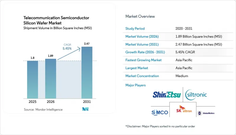
An industry pivot toward 5G massive-MIMO base stations, early 6G research platforms, and silicon photonics transceivers is redefining substrate purity, diameter, and defect-density requirements. Government CHIPS-style incentives, particularly in the United States, the European Union, Japan, and South Korea, are encouraging domestic wafer-fab construction, shortening supply chains that were historically concentrated in East Asia. Consolidation among six global suppliers is reinforcing an oligopolistic pricing structure, while new Chinese entrants remain capacity-constrained by export controls on sub-14-nanometer equipment. At the same time, stricter environmental regulations on slurry waste and escalating capital intensity are putting pressure on cost structures, nudging the telecommunication semiconductor silicon wafer market toward higher value specialty substrates.
Global Telecommunication Semiconductor Silicon Wafer Market Trends and Insights
Surging 5G/6G Base-Station Deployments Demanding High-Purity 300 mm Wafers
Massive-MIMO base stations require gallium-nitride power amplifiers and silicon RF front-ends fabricated on 300 mm substrates that must exceed 1,000 ohm-centimeter resistivity to limit substrate losses at frequencies above 3.5 GHz. Global silicon wafer shipments climbed to 12.973 billion square inches in 2025, largely driven by telecom demand. Imec validated GaN-on-silicon RF transistors operating in the 7-24 GHz band, designated for 6G, extending wafer consumption beyond current 5G needs. China Mobile and China Telecom deployed a combined 1.2 million 5G sites by 2025, each using roughly 200-300 square inches of silicon. Only two suppliers consistently meet the parts-per-trillion metallic contamination threshold required for millimeter-wave applications.
Government CHIPS-Style Incentives Accelerating Telecom-Centric Wafer Fabs
The US CHIPS and Science Act reserved USD 36.4 billion across 40 projects by 2025, with GlobalWafers obtaining USD 400 million for twin 300 mm plants in Texas and Missouri. Texas Instruments secured USD 1.6 billion in funding, earmarked for four 300 mm fabs that feed base-station backhaul and power-supply ICs. Europe committed EUR 43 billion (USD 46 billion) under its Chips Act, underwriting Infineon and STMicroelectronics' capacity for RF and power wafers. Japan's JPY 920 billion (USD 6.2 billion) subsidy package is ensuring 300 mm substrate availability for 5G despite geopolitical frictions. These grants lower effective capital costs 25-35%, compressing payback times to under 10 years.
Capital Intensity and Long Payback Periods for 300 mm Wafer Lines
A single greenfield 300 mm plant costs USD 3-5 billion, with equipment absorbing up to 70% of outlay. Siltronic's Singapore expansion illustrates the challenge, spending EUR 2 billion (USD 2.14 billion) for 1 million wafers per year. Even entrenched firms like SUMCO and SK Siltron formed a joint venture to share a USD 3.6 billion build-out. Where subsidies cover less than 15% of costs, investors face 10-15 year payback horizons, deterring new entrants and reinforcing the oligopoly.
Other drivers and restraints analyzed in the detailed report include:
- Rapid Adoption of Silicon Photonics Transceivers Boosting SOI Wafer Demand
- Expansion of 300 mm Capacity for Cloud and Edge Data-Traffic Processors
- Defect-Density Challenges with High-Resistivity RF-Grade Wafers
For complete list of drivers and restraints, kindly check the Table Of Contents.
Segment Analysis
The 300 mm segment controlled 64.48% of volume in 2025, reflecting per-die savings of 30-40% and automation advantages. GlobalWafers' Sherman site shipped its first 1.2 million wafers in 2025, underscoring domestic momentum. Texas Instruments joined with four 40,000-wspm modules to feed analog and embedded telecom ICs. Equipment shortages keep 200 mm capacity tight, nudging redesigns onto 300 mm lines. Sub-150-mm wafers remain a niche for GaN power RF amplifiers and MEMS antenna tuners, yet continue to cede market share. Regulatory bodies have little sway over diameter choice, though export controls on 300 mm tools to China slow adoption there.
As chiplet architectures rise, each radio front-end now requires multiple dies across power, RF, and digital domains, inflating demand for larger substrates. The telecommunication semiconductor silicon wafer market sees suppliers bundling prime-polished and epitaxial variants to lock in volume. Industry consortia like SEMI standardize notch positions and thickness tolerances, allowing fabs to quickly qualify multiple sources, which tempers supplier power marginally but keeps barriers high for new entrants.
The Telecommunication Semiconductor Silicon Wafer Market Report is Segmented by Wafer Diameter (Up To 150 Mm, 200 Mm, and 300 Mm), Semiconductor Device Type (Logic, Memory, Analog, and More), Wafer Type (Prime Polished, Epitaxial, Silicon-On-Insulator (SOI), and More), and Geography. The Market Forecasts are Provided in Terms of Volume (Square Inches).
Geography Analysis
Asia-Pacific supplied 80.11% of wafers in 2025 and posts a 6.78% CAGR to 2031. China's 1.2 million 5G base stations create captive demand that domestic suppliers rush to serve, though tool embargoes keep yields below Japanese levels. Japan's Shin-Etsu and SUMCO together furnish about 55% of global 300 mm capacity, leveraging unmatched Czochralski expertise. South Korea's SUMCO-SK Siltron venture adds 1 million wafers annually by 2027, with telecom and automotive as anchor segments. Taiwan remains a voracious consumer through foundry leader TSMC, whose Kumamoto site secures JPY 920 billion (USD 6.2 billion) state backing.
North America gains momentum from USD 36.4 billion CHIPS Act funding. GlobalWafers and Texas Instruments collectively deliver 2 million 300 mm wafers by 2027, trimming reliance on Asian imports. Europe's EUR 43 billion (USD 46 billion) Chips Act bankrolls Infineon and STMicroelectronics expansions, yet its share lingers below 10% because of elevated energy and labor costs. South America and the Middle East and Africa remain small, importing wafers for limited 5G rollouts.
Export controls by the United States, Japan, and the Netherlands on sub-14 nm equipment fragment the Asia-Pacific chain, forcing Chinese fabs onto 28 nm and enlarging wafer area per function by up to 60%. China's retaliatory curbs on gallium and germanium raise compound-semiconductor costs, shifting demand to Japanese and Korean suppliers that enjoy diversified feedstock. Supply-chain diversification efforts will show material impact only after 2030 due to 10-15 year payback cycles for new fabs.
- Shin-Etsu Chemical Co., Ltd.
- SUMCO Corporation
- GlobalWafers Co., Ltd.
- Siltronic AG
- SK Siltron Co., Ltd.
- Soitec SA
- National Silicon Industry Group Co., Ltd.
- Wafer Works Corp.
- Hangzhou Semiconductor Wafer Co., Ltd.
- Ferrotec Holdings Corp.
- Okmetic Oyj
- MEMC Electronic Materials, Inc.
- Zhonghuan Semiconductor Co., Ltd.
- GRINM Semiconductor Materials Co., Ltd.
- Shanghai Advanced Silicon Technology Co., Ltd.
- MCL Electronic Materials Ltd.
- Simgui (Shanghai) Technology Co., Ltd.
- AST Photoelectricity Co., Ltd.
- LG Siltron Advanced Materials, Inc.
- NSIG (Shanghai) Silicon Technologies Co., Ltd.
Additional Benefits:
- The market estimate (ME) sheet in Excel format
- 3 months of analyst support
TABLE OF CONTENTS
1 INTRODUCTION
- 1.1 Study Assumptions and Market Definition
- 1.2 Scope of the Study
2 RESEARCH METHODOLOGY
3 EXECUTIVE SUMMARY
4 MARKET LANDSCAPE
- 4.1 Market Overview
- 4.2 Industry Value-Chain Analysis
- 4.3 Regulatory Landscape
- 4.4 Technology Analysis
- 4.5 Impact of Macroeconomic Factors on the Market
- 4.6 Porter's Five Forces Analysis
- 4.6.1 Bargaining Power of Suppliers
- 4.6.2 Bargaining Power of Buyers
- 4.6.3 Threat of New Entrants
- 4.6.4 Threat of Substitutes
- 4.6.5 Intensity of Competitive Rivalry
- 4.7 Market Drivers
- 4.7.1 Surging 5G/6G Base-Station Deployments Demanding High-Purity 300 mm Wafers
- 4.7.2 Government CHIPS-Style Incentives Accelerating Telecom-Centric Wafer Fabs
- 4.7.3 Rapid Adoption of Silicon Photonics Transceivers Boosting SOI Wafer Demand
- 4.7.4 Expansion of 300 mm Capacity for Cloud and Edge Data-Traffic Processors
- 4.7.5 Ultra-Thin Wafer Demand for Co-Packaged Optics Driving New Grinding Chemistries
- 4.7.6 Back-Side Power-Delivery Ready Wafers for AI-Powered Base-Station SoCs
- 4.8 Market Restraints
- 4.8.1 Capital Intensity and Long Payback Periods for 300 mm Wafer Lines
- 4.8.2 Defect-Density Challenges with High-Resistivity RF-Grade Wafers
- 4.8.3 Export-Control Restrictions on Advanced Wafer-Equipment Shipments
- 4.8.4 Stricter Slurry-Waste Regulations Impacting Photonics-Grade CMP Costs
5 MARKET SIZE AND GROWTH FORECASTS (VOLUME)
- 5.1 By Wafer Diameter
- 5.1.1 Up to 150 mm
- 5.1.2 200 mm
- 5.1.3 300 mm
- 5.2 By Semiconductor Device Type
- 5.2.1 Logic
- 5.2.2 Memory
- 5.2.3 Analog
- 5.2.4 Discrete
- 5.2.5 Other Semiconductor Device Types (Optoelectronics, Sensors, Micro)
- 5.3 By Wafer Type
- 5.3.1 Prime Polished
- 5.3.2 Epitaxial
- 5.3.3 Silicon-on-Insulator (SOI)
- 5.3.4 Specialty Silicon (High-Resistivity, Power, Sensor-Grade)
- 5.4 By Geography
- 5.4.1 North America
- 5.4.1.1 United States
- 5.4.1.2 Canada
- 5.4.1.3 Mexico
- 5.4.2 Europe
- 5.4.2.1 Germany
- 5.4.2.2 United Kingdom
- 5.4.2.3 France
- 5.4.2.4 Rest of Europe
- 5.4.3 Asia-Pacific
- 5.4.3.1 China
- 5.4.3.2 Japan
- 5.4.3.3 India
- 5.4.3.4 South Korea
- 5.4.3.5 Taiwan
- 5.4.3.6 Rest of Asia-Pacific
- 5.4.4 South America
- 5.4.5 Middle East
- 5.4.6 Africa
- 5.4.1 North America
6 COMPETITIVE LANDSCAPE
- 6.1 Market Concentration
- 6.2 Strategic Moves
- 6.3 Market Share Analysis
- 6.4 Company Profiles (includes Global Level Overview, Market Level Overview, Core Segments, Financials as available, Strategic Information, Market Rank/Share, Products and Services, Recent Developments)
- 6.4.1 Shin-Etsu Chemical Co., Ltd.
- 6.4.2 SUMCO Corporation
- 6.4.3 GlobalWafers Co., Ltd.
- 6.4.4 Siltronic AG
- 6.4.5 SK Siltron Co., Ltd.
- 6.4.6 Soitec SA
- 6.4.7 National Silicon Industry Group Co., Ltd.
- 6.4.8 Wafer Works Corp.
- 6.4.9 Hangzhou Semiconductor Wafer Co., Ltd.
- 6.4.10 Ferrotec Holdings Corp.
- 6.4.11 Okmetic Oyj
- 6.4.12 MEMC Electronic Materials, Inc.
- 6.4.13 Zhonghuan Semiconductor Co., Ltd.
- 6.4.14 GRINM Semiconductor Materials Co., Ltd.
- 6.4.15 Shanghai Advanced Silicon Technology Co., Ltd.
- 6.4.16 MCL Electronic Materials Ltd.
- 6.4.17 Simgui (Shanghai) Technology Co., Ltd.
- 6.4.18 AST Photoelectricity Co., Ltd.
- 6.4.19 LG Siltron Advanced Materials, Inc.
- 6.4.20 NSIG (Shanghai) Silicon Technologies Co., Ltd.
7 MARKET OPPORTUNITIES AND FUTURE OUTLOOK
- 7.1 White-Space and Unmet-Need Assessment
