|
시장보고서
상품코드
2044002
IoT 반도체 실리콘 웨이퍼 : 시장 점유율 분석, 업계 동향 및 통계, 성장 예측(2026-2031년)IoT Semiconductor Silicon Wafer - Market Share Analysis, Industry Trends & Statistics, Growth Forecasts (2026 - 2031) |
||||||
 Mordor Intelligence
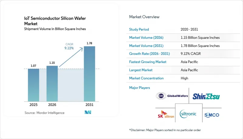
IoT 반도체 실리콘 웨이퍼 시장 규모는 2025년 10억 7,000만 평방인치로 평가되었습니다. 2026년에는 11억 5,000만 평방인치로 확대되어 2031년까지 17억 8,000만 평방인치에 이를 것으로 예상되며 2026-2031년에 걸쳐 CAGR 9.12%를 나타낼 전망입니다.
엣지 AI 추론으로의 구조적 변화로 인해 설계는 기존 지오메트리에서 고급 노드 처리로 이동하고 있으며, 웨이퍼 수요와 컴퓨팅 밀도의 연관성이 강화되고 있습니다. 미국과 유럽의 정책적 인센티브로 인해 국내 300mm 제조 시설에 새로운 자본이 유입되고 있으며, 아시아태평양공급망에 대한 의존도가 점차 감소하고 있습니다. 자동차 및 산업용 OEM 업체들이 체결한 장기 공급 계약에 따라 성숙 노드와 최첨단 노드 모두에서 공급이 확보되어 전체 직경 등급에서 높은 가동률을 지원하는 이중 구조 수요 프로파일을 형성하고 있습니다. 동시에, 폴리실리콘 가격 변동과 재생 200mm 장비의 부족으로 인해 비용 압박이 계속되고 있으며, IoT 반도체 실리콘 웨이퍼 시장 전체에서 전략적 재고 버퍼의 필요성이 더욱 커지고 있습니다.
세계의 IoT 반도체 실리콘 웨이퍼 시장 동향과 인사이트
파운드리의 300mm 생산능력 대폭 확대
파운드리 업체들은 2024-2026년 초까지 300mm 팹에 1,500억 달러 이상을 투자하고, 미국, 대만, 한국, 독일에 대규모 클린룸을 증설할 예정입니다. 이러한 메가팹은 다이 수율 향상과 자동화 수준 향상을 통해 웨이퍼당 비용을 크게 절감하고, 수익성을 훼손하지 않고 공정 미세화 로드맵을 추진할 수 있게 해줍니다. 300mm로의 전환에 따른 장비 전환으로 사용 가능한 200mm용 장비공급도 감소하고 있으며, 이로 인해 장비 브로커의 가격 결정력이 강화되고 있습니다. 첨단 자동차용 및 산업용 로직에 대한 고객 수요는 이미 양산 전 단계에 이르렀으며, 생산 능력과 복잡성이 동시에 증가함에 따라 IoT 반도체 실리콘 웨이퍼 시장이 어떻게 혜택을 받을 수 있는지를 잘 보여주고 있습니다.
엣지 AI 지원 IoT 디바이스로 인한 고급 노드에 대한 수요 증가
스마트 카메라, 예지보전 모듈, 의료용 웨어러블 기기에는 현재 추론을 로컬에서 실행하는 뉴럴 코어가 내장되어 있어 지연 시간을 단축하고 프라이버시 우려를 피할 수 있습니다. 주력인 4nm 프로세서는 48 TOPS의 성능을 발휘하면서도 소비전력이 5W 이하로, 28nm 이상의 노드에서는 달성할 수 없는 전력 대 성능 비율입니다. 유럽과 북미의 데이터 보호법이 강화되는 가운데, OEM 업체들은 단가가 상승하더라도 첨단 공정 웨이퍼로의 전환을 가속화하고 있습니다. 파운드리 측도 엣지 AI 고객을 위해 7nm 이하의 생산 능력을 우선적으로 고려하고 있습니다. 이는 다이 수율의 학습 곡선이 가파르고 평방인치당 수익이 높아지기 때문입니다. 이러한 선순환이 IoT 반도체 실리콘 웨이퍼 시장의 CAGR을 크게 끌어올리고 있습니다.
재생 200mm 팹 장비 부족
OEM 업체들은 10년 전 200mm용 장비의 신규 생산을 중단했기 때문에 성숙 노드 생산을 지속하는 팹은 폐기된 라인에서 장비를 회수하고 있습니다. 에칭 장비와 CVD 장비의 브로커 가격은 2023년 이후 두 배로 뛰었고, 자동차 안전 표준에 따른 재인증 프로토콜로 인해 리드 타임은 2년까지 늘어났습니다. 이 설비의 병목현상으로 인해 최종 시장의 주문이 견조함에도 불구하고, 전력관리 IC와 MEMS 센서의 성장 상한선이 제한되어 IoT 반도체 실리콘 웨이퍼 시장의 모멘텀이 둔화되고 있습니다.
부문 분석
2025년 기준, 200mm 부문은 IoT 반도체 실리콘 웨이퍼 시장 점유율의 57.33%를 차지하며, 감가상각이 완료된 장비 세트에서 작동하는 파워 디바이스 및 MEMS 센서에 대한 지속적인 수요를 나타냈습니다. 그럼에도 불구하고,300mm의 출하량은 2031년까지 연평균 복합 성장률(CAGR) 10.43%를 나타낼 것으로 예측됩니다. 이는 웨이퍼 한 장당 2배 이상의 다이를 생산할 수 있고, 마스크와 장비의 비용을 더 많은 생산량에 분산시킬 수 있다는 경제적 계산을 반영한 것입니다. 따라서 300mm 노드 관련 IoT 반도체 실리콘 웨이퍼 시장 규모는 산업 전체 생산량 성장률보다 빠른 속도로 확대되고 있습니다.
재무구조가 탄탄한 아시아 파운드리 업체들은 200mm 모듈을 300mm로 일제히 전환하고 있으며, 이로 인해 구식 설비가 재판매용으로 풀려나면서, 유사한 자본적 인센티브가 없는 지역에서는 공급 부족이 심화되고 있습니다. 유럽 팹은 자동차 산업 고객이 최첨단 집적도보다 공급망 친숙도를 더 중요시하기 때문에 200mm 자산을 계속 활용하고 있습니다. 그러나 시간이 지남에 따라 파워 디바이스 라인도 더 긴 다이 채널과 더 높은 정격 전류를 실현하기 위해 300mm 기판을 채택하고 있으며, 이러한 변화로 인해 IoT 반도체 실리콘 웨이퍼 시장은 지속적으로 진화하고 있습니다.
"IoT 반도체 실리콘 웨이퍼 시장 보고서는 웨이퍼 직경(300mm 및 200mm), 기술 노드(첨단 노드, 메인스트림 노드, 성숙 노드), 최종 용도(소비자 IoT, 산업용 IoT, 헬스케어 IoT, 인프라/스마트시티 IoT), 지역(북미, 유럽, 아시아태평양, 기타)별로 분류하여 분석하였습니다. 아시아태평양, 기타) 별로 분류되어 있습니다. 시장 예측은 출하량(평방인치)으로 제공됩니다.
지역별 분석
아시아태평양은 2025년 69.84%의 시장 점유율로 1위를 차지했고, 2031년까지 연평균 10.91%의 성장률을 나타낼 것으로 예측되며, 세계 첨단 노드 생산 능력의 핵심인 대만과 한국의 메가팹에 힘입어 2031년까지 연평균 복합 성장률(CAGR) 10.91%로 성장할 것으로 전망됩니다. 중국의 보조금 확대에 따라 28nm 이상 공정에서는 공급량이 증가하고 있지만, 최첨단 미세화 공정의 수율 문제로 인해 수입 의존도는 여전히 높은 수준입니다. 일본 웨이퍼 공급업체들은 지리적 근접성과 장기 계약을 통해 협상력을 유지하고 있으며, 인도 백엔드에 대한 투자는 새로운 다운스트림 수요를 창출하고 있습니다.
북미는 공급량에서 차지하는 비중은 작지만, 정책적 측면에서 큰 호재로 작용하고 있습니다. CHIPS 법은 애리조나 주와 오하이오 주에 새로운 공장 건설에 자금을 지원하고 있으며, 3nm 로직과 성숙한 노드 아날로그 모두를 대상으로 2031년까지 IoT 반도체 실리콘 웨이퍼 시장을 아시아와 기타 지역의 비율을 60 대 40으로 점차 재조정하고 있습니다. 국내 고객, 특히 항공우주 및 방산 부문 OEM은 현지 조달 조항을 충족하기 위해 이러한 팹을 우선시하고 있으며, 이는 향후 가동률을 뒷받침하고 있습니다.
유럽은 자동차 OEM이 기능 안전상의 이유로 현지 웨이퍼 공급을 확보했기 때문에 여전히 큰 점유율을 유지하고 있습니다. 정부의 보조금 지원으로 EV 및 산업용 제어 수요에 대응하기 위해 40nm에서 90nm의 파워 디바이스에 초점을 맞춘 드레스덴과 그르노블의 확장이 가속화되고 있습니다. 유럽 거점 중 5nm 이하 생산을 확정한 곳은 없지만, 공동 사업을 통해 마스크 및 포토레지스트 노하우를 도입하여 동 지역이 세계 IoT 반도체 실리콘 웨이퍼 시장에서 존재감을 유지할 수 있도록 노력하고 있습니다.
기타 혜택
- 엑셀 형태 시장 예측(ME) 시트
- 3개월간 애널리스트 지원
자주 묻는 질문
목차
제1장 서론
제2장 조사 방법
제3장 주요 요약
제4장 시장 구도
제5장 시장 규모와 성장 예측(지역별 출하량)
제6장 경쟁 구도
제7장 시장 기회와 향후 전망
KTHThe IoT semiconductor silicon wafer market size is expected to increase from 1.07 billion square inches in 2025 to 1.15 billion square inches in 2026 and reach 1.78 billion square inches by 2031, growing at a CAGR of 9.12% over 2026-2031.
A structural shift toward edge-AI inference is steering designs from legacy geometries to advanced-node processing, tightening the link between wafer demand and compute density. Policy incentives in the United States and Europe are channeling fresh capital into domestic 300 mm facilities, gradually diluting the region's dependence on Asia-Pacific supply chains. Long-term supply pacts signed by automotive and industrial OEMs are locking in allocations at both mature and leading-edge nodes, creating a two-tier demand profile that supports high utilization across diameter classes. At the same time, polysilicon price swings and a scarcity of refurbished 200 mm tools keep cost pressure elevated, reinforcing the need for strategic inventory buffers throughout the IoT semiconductor silicon wafer market.
Global IoT Semiconductor Silicon Wafer Market Trends and Insights
Surging 300 mm Capacity Expansion Among Foundries
Foundries committed more than USD 150 billion to 300 mm fabs from 2024 to early 2026, adding high-volume clean-rooms in the United States, Taiwan, South Korea, and Germany. These mega-fabs slash cost per wafer by leveraging larger die yields and higher automation levels, allowing process shrink roadmaps to proceed without eroding margins. Equipment cascades from 300 mm conversions also shrink the pool of usable 200 mm tools, fortifying pricing power for machinery brokers. Customer demand for advanced automotive and industrial logic has already filled pre-production slots, underscoring how the IoT semiconductor silicon wafer market benefits when capacity and complexity rise in tandem.
Advanced-Node Demand From Edge-AI Enabled IoT Devices
Smart cameras, predictive-maintenance modules, and medical wearables now embed neural cores that deliver inference locally, cutting latency and sidestepping privacy concerns. A flagship 4 nm processor draws under 5 W while pushing 48 TOPS, a power-performance point unattainable on 28 nm or larger nodes. As data-protection laws tighten in Europe and North America, OEMs accelerate the pivot to advanced wafers even when unit costs rise. Foundries, for their part, prioritize sub-7 nm capacity for edge-AI customers because die-yield learning curves are steeper, boosting revenue per square inch. This virtuous loop adds meaningful lift to the IoT semiconductor silicon wafer market CAGR.
Scarcity of Refurbished 200 mm Fab Tools
OEMs halted new 200 mm tool production a decade ago, so fabs extending mature nodes scavenge decommissioned lines. Broker prices for etchers and CVD gear have doubled since 2023, while requalification protocols mandated by automotive safety standards stretch lead times to two years. This equipment bottleneck caps the growth ceiling for power-management ICs and MEMS sensors despite robust end-market orders, trimming momentum in the IoT semiconductor silicon wafer market.
Other drivers and restraints analyzed in the detailed report include:
- Government Chip Incentives (CHIPS and EU Chips Acts)
- Rising Adoption of 200 mm Wafers for Power and MEMS IoT Chips
- Geopolitical Export Controls on Advanced Nodes
For complete list of drivers and restraints, kindly check the Table Of Contents.
Segment Analysis
The 200 mm segment controlled 57.33% of IoT semiconductor silicon wafer market share in 2025, illustrating the endurance of power devices and MEMS sensors that thrive on depreciated toolsets. Nevertheless, 300 mm shipments are projected to climb at a 10.43% CAGR to 2031, reflecting an economic calculus in which each larger wafer yields more than twice the dies, spreading mask and equipment costs across greater output. The IoT semiconductor silicon wafer market size tied to 300 mm nodes is therefore expanding faster than overall industry volume growth.
Asian foundries with deep balance sheets are converting 200 mm modules en masse, freeing legacy gear for resale yet amplifying scarcity in regions without similar capital incentives. European fabs continue to sweat 200 mm assets because automotive clients prize supply-chain familiarity over leading-edge density. Over time, however, power-device lines are also adopting 300 mm substrates to access longer die channels and higher current ratings, a shift that keeps the IoT semiconductor silicon wafer market in continuous evolution.
The IoT Semiconductor Silicon Wafer Market Report is Segmented by Wafer Diameter (300 Mm and 200 Mm), Technology Node (Advanced Node, Mainstream Node, and Mature Node), End Application (Consumer IoT, Industrial IoT, Healthcare IoT, and Infrastructure/Smart City IoT), and Geography (North America, Europe, Asia-Pacific, and More). The Market Forecasts are Provided in Terms of Shipment Volume (Square Inches).
Geography Analysis
Asia-Pacific dominated with 69.84% of the market share in 2025 and is projected to grow at 10.91% CAGR through 2031, underpinned by Taiwanese and South Korean mega-fabs that anchor global advanced-node capacity. China's subsidized expansions add bulk at 28 nm and above, but yield hurdles at cutting-edge geometries keep import dependence high. Japanese wafer suppliers leverage proximity and long-term contracts to maintain bargaining leverage, while India's back-end investments create fresh downstream demand.
North America is contributing a smaller share of the volume but is receiving significant policy momentum. The CHIPS Act funds greenfield sites in Arizona and Ohio, targeting both 3 nm logic and mature-node analog, gradually rebalancing the IoT semiconductor silicon wafer market toward a 60-40 Asia-rest-of-world split by 2031. Domestic customers, especially aerospace and defense OEMs, prioritize these fabs to satisfy local-content clauses, anchoring future utilization.
Europe maintained a significant share as automotive OEMs secured local wafer supply for functional-safety reasons. Government grants accelerate Dresden and Grenoble expansions focused on 40-nm to 90-nm power devices to address EV and industrial control demand. While no European site has committed to sub-5 nm production, collaborative ventures aim to import masks and photoresist know-how, ensuring the region retains relevance within the global IoT semiconductor silicon wafer market.
- Shin-Etsu Chemical Co. Ltd.
- SUMCO Corporation
- GlobalWafers Co. Ltd.
- Siltronic AG
- SK Siltron Co. Ltd.
- Soitec SA
- National Silicon Industry Group Co. Ltd.
- Zhonghuan Advanced Semiconductor Materials Co. Ltd.
- Wafer Works Corp.
- Hangzhou Silicon Wafer Co. Ltd.
- Okmetic Oy j
- Taiwan Semiconductor Manufacturing Co. Ltd.
- Samsung Electronics Co. Ltd. Foundry Division
- United Microelectronics Corporation
- GlobalFoundries Inc.
- Tower Semiconductor Ltd.
- Nexchip Semiconductor Corporation
- X-FAB Silicon Foundries SE
Additional Benefits:
- The market estimate (ME) sheet in Excel format
- 3 months of analyst support
TABLE OF CONTENTS
1 INTRODUCTION
- 1.1 Study Assumptions and Market Definition
- 1.2 Scope of the Study
2 RESEARCH METHODOLOGY
3 EXECUTIVE SUMMARY
4 MARKET LANDSCAPE
- 4.1 Market Overview
- 4.2 Market Drivers
- 4.2.1 Surging 300 mm Capacity Expansion Among Foundries
- 4.2.2 Advanced-Node Demand From Edge-AI Enabled IoT Devices
- 4.2.3 Government Chip Incentives CHIPS and EU Chips Acts
- 4.2.4 Rising Adoption of 200 mm Wafers for Power and MEMS IoT Chips
- 4.2.5 Strategic Long-Term Supply Agreements With Automotive IoT OEMs
- 4.2.6 Sustainability Requirements Driving Low-Defect Wafer Processes
- 4.3 Market Restraints
- 4.3.1 Scarcity of Refurbished 200 mm Fab Tools
- 4.3.2 Geopolitical Export Controls on Advanced Nodes
- 4.3.3 High Capital Outlay for Below 7 nm Wafer Production
- 4.3.4 Volatile Polysilicon and Specialty Gas Pricing
- 4.4 Industry Supply-Chain Analysis
- 4.5 Regulatory Landscape
- 4.6 Technological Outlook
- 4.7 Impact of Macroeconomic Factors on the Market
- 4.8 Porter's Five Forces Analysis
- 4.8.1 Threat of New Entrants
- 4.8.2 Bargaining Power of Suppliers
- 4.8.3 Bargaining Power of Buyers
- 4.8.4 Threat of Substitutes
- 4.8.5 Intensity of Competitive Rivalry
5 MARKET SIZE AND GROWTH FORECASTS (SHIPMENT BY AREA)
- 5.1 By Wafer Diameter
- 5.1.1 300 mm
- 5.1.2 200 mm
- 5.2 By Technology Node
- 5.2.1 Advanced Node (Below 7nm)
- 5.2.2 Mainstream Node (10nm-28nm)
- 5.2.3 Mature Node (Above 28nm)
- 5.3 By End Application
- 5.3.1 Consumer IoT
- 5.3.2 Industrial IoT
- 5.3.3 Healthcare IoT
- 5.3.4 Infrastructure / Smart City IoT
- 5.4 By Geography
- 5.4.1 North America
- 5.4.1.1 United States
- 5.4.1.2 Canada
- 5.4.1.3 Mexico
- 5.4.2 Europe
- 5.4.2.1 Germany
- 5.4.2.2 United Kingdom
- 5.4.2.3 France
- 5.4.2.4 Rest of Europe
- 5.4.3 Asia-Pacific
- 5.4.3.1 China
- 5.4.3.2 Japan
- 5.4.3.3 India
- 5.4.3.4 South Korea
- 5.4.3.5 Taiwan
- 5.4.3.6 Rest of Asia-Pacific
- 5.4.4 South America
- 5.4.5 Middle East and Africa
- 5.4.1 North America
6 COMPETITIVE LANDSCAPE
- 6.1 Market Concentration
- 6.2 Strategic Moves
- 6.3 Market Share Analysis
- 6.4 Company Profiles (includes Global level Overview, Market Level Overview, Core Segments, Financials as Available, Strategic Information, Market Rank/Share for Key Companies, Products and Services, and Recent Developments)
- 6.4.1 Shin-Etsu Chemical Co. Ltd.
- 6.4.2 SUMCO Corporation
- 6.4.3 GlobalWafers Co. Ltd.
- 6.4.4 Siltronic AG
- 6.4.5 SK Siltron Co. Ltd.
- 6.4.6 Soitec SA
- 6.4.7 National Silicon Industry Group Co. Ltd.
- 6.4.8 Zhonghuan Advanced Semiconductor Materials Co. Ltd.
- 6.4.9 Wafer Works Corp.
- 6.4.10 Hangzhou Silicon Wafer Co. Ltd.
- 6.4.11 Okmetic Oy j
- 6.4.12 Taiwan Semiconductor Manufacturing Co. Ltd.
- 6.4.13 Samsung Electronics Co. Ltd. Foundry Division
- 6.4.14 United Microelectronics Corporation
- 6.4.15 GlobalFoundries Inc.
- 6.4.16 Tower Semiconductor Ltd.
- 6.4.17 Nexchip Semiconductor Corporation
- 6.4.18 X-FAB Silicon Foundries SE
7 MARKET OPPORTUNITIES AND FUTURE OUTLOOK
- 7.1 White-Space and Unmet-Need Assessment