
|
시장보고서
상품코드
2044008
가전제품용 반도체 실리콘 웨이퍼 : 시장 점유율 분석, 업계 동향 및 통계, 성장 예측(2026-2031년)Consumer Electronics Semiconductor Silicon Wafer - Market Share Analysis, Industry Trends & Statistics, Growth Forecasts (2026 - 2031) |
||||||
가전제품용 반도체 실리콘 웨이퍼 시장 규모는 2025년 52억 3,000만 평방인치로 평가되었습니다. 2026년 54억 5,000만 평방인치로부터, 2031년까지 68억 3,000만 평방인치로 확대되며 2026년부터 2031년까지 연평균 복합 성장률(CAGR)은 4.61%를 나타낼 전망입니다.

로직 집적도가 높은 디바이스에 대한 수요 증가, 첨단 노드로의 전환, 정부 주도의 팹 지원 정책 등이 이러한 성장의 원동력이 되고 있습니다. 주요 파운드리 업체들의 설비투자는 여전히 다이 수를 최대화할 수 있는 300mm 기판에 집중되고 있지만, 실리콘 온 인슐레이터(SOI) 등 특수 웨이퍼는 5G 스마트폰에서 더 높은 무선 주파수 효율을 구현할 수 있어 점유율을 확대되고 있습니다. 한편, 아날로그 및 개별 장치가 성숙한 공정 노드에 머물러 있기 때문에 구세대 200mm 생산 능력은 지속적인 수익률 압박에 직면하고 있습니다. 미국과 유럽에서 지역 분산화가 진행되고 있지만, 아태지역은 비용, 기존 공급망 및 설치된 웨이퍼 생산 능력에서 구조적 우위를 유지하고 있습니다.
세계의 가전제품용 반도체 실리콘 웨이퍼 시장 동향과 인사이트
5G 지원 스마트폰 보급
휴대폰 업체는 여러 개의 6GHz 이하 및 mm파 프론트엔드 모듈을 탑재하고 있으며, 각 모듈에는 저잡음 증폭기 및 전력 증폭기용 개별 다이가 포함되어 있습니다. 퀄컴의 Snapdragon 8 Elite는 첨단 4nm 공정으로 제조되며, 기존 LTE 플랫폼에 비해 디바이스 당 약 30% 더 많은 웨이퍼 면적을 할당하고 있습니다. 중국과 인도에서는 독립형 5G 네트워크가 구축되어 전 세계 출하량 증가에도 불구하고 웨이퍼 수요를 뒷받침하고 있습니다. 고주파용 SOI 기판은 신호 손실을 감소시켜 SOI 웨이퍼의 CAGR 5.31%를 뒷받침하는 프리미엄 가격 책정을 가능하게 합니다. 질화갈륨이나 인듐 인화물 증폭기로 부분적인 대체가 진행되고 있지만, 실리콘 수요 증가를 둔화시킬 수는 있지만, 그 흐름을 방해하지는 않습니다.
대용량 모바일 스토리지(3D NAND)의 성장
512GB 및 1TB급 용량을 탑재한 스마트폰의 등장으로 232단 NAND 스택으로의 전환이 가속화되어 웨이퍼의 시작 횟수와 재작업 주기가 증가했습니다. 2025년 하반기에 보고된 공급 부족으로 인해 1Tb 다이 방식의 조기 채택이 진행되어 출하되는 테라바이트당 실리콘 소비량이 증가했습니다. 동시에 삼성과 SK하이닉스는 300mm 라인을 대용량 메모리로 전환하면서 민수용 낸드 공급을 압박하고 웨이퍼의 평균 판매 가격을 끌어올렸습니다. 이로 인한 수요 급증은 수율 학습 곡선이 성숙하고 새로운 생산 능력이 가동되기 시작하면서 2년 이내에 정점에 도달할 것입니다.
자본 집약적인 대구경 결정 성장
풀링기, 슬라이싱 톱, 계측장비 등을 포함하면 300mm 초크랄스키법 라인 1대의 비용은 4억 달러가 넘을 수 있습니다. 설비 리드타임이 2년을 초과하는 경우가 많아 경기 상승 국면에서 신규 생산능력의 가동이 늦어지고 있습니다. 실트로닉이 2026년에 예상하는 한 자릿수 중반의 매출 감소는 재고 소화의 장기화와 설비투자 지연이 고정비 부담을 얼마나 가중시키고 있는지를 잘 보여줍니다. SUMCO가 2026년 말까지 미야자키의 200mm 공장을 폐쇄할 계획은 기존의 과잉 생산 능력과 설비 갱신에 따른 자본 부담을 반영하고 있습니다. 북미와 유럽의 인건비와 에너지 비용의 상승은 손익분기점을 더욱 높여 이러한 제약을 더욱 강화시키고 있습니다.
부문 분석
2025년, 300mm급은 가전제품용 반도체 실리콘 웨이퍼 시장 점유율의 71.29%를 차지했습니다. 이는 높은 설비 비용보다 웨이퍼 당 다이 수에서 우수한 경제성을 반영하고 있습니다. 파운드리 업체들이 3nm 및 게이트 올 어라운드(GaAA) 노드를 위해 사상 최대 규모의 설비 투자를 진행하면서, 이 부문은 전체 시장에서 4.61%의 연평균 복합 성장률(CAGR)을 나타내고, 성장 곡선을 그리며 성장세를 이어가고 있습니다. TSMC만 해도 2026년 확장 계획에 520억-560억 달러를 책정했는데, 이 중 거의 전액이 300mm 팹에 투입됩니다. 300mm 플랫폼용 가전제품용 반도체 실리콘 웨이퍼 시장 규모는 2031년까지 49억 평방인치에 달할 것으로 예측됩니다.
새로운 박형화 및 본딩 기술로 인해 50µ&m 미만의 300mm 기판이 가능해져 과거에는 더 작은 직경의 기판에 국한되어 있던 응용 분야가 확대되고 있습니다. 반면, 공정 전환의 이점이 제한적인 아날로그, MEMS, 파워디스크리트 분야에서는 200mm 라인이 여전히 존재하고 있습니다. 150mm 미만의 웨이퍼는 주로 고저항 RF 스위치나 특수 센서와 같은 틈새 시장으로 이동하고 있습니다. SUMCO의 미야자키 공장 폐쇄를 포함한 공급 합리화로 프리미엄급 300mm 생산량 증가에도 불구하고 레거시 노드의 가격 안정화에 기여하고 있습니다.
"가전제품용 반도체 실리콘 웨이퍼 시장 보고서는 웨이퍼 직경(150mm 이하, 200mm, 300mm), 반도체 디바이스 유형(로직, 메모리 등), 웨이퍼 유형(프라임 폴리싱, 에피택셜, 특수 실리콘 등), 지역(북미, 유럽, 아시아, 아시아태평양, 남미, 중동 및 아프리카) 별로 분류하여 분석하였습니다. 태평양, 남미, 중동 및 아프리카)로 분류됩니다. 시장 예측은 출하량(평방인치)으로 표시됩니다.
지역별 분석
아시아태평양은 2025년 출하량의 84.78%를 차지하며 가전제품용 반도체 실리콘 웨이퍼 시장에서 선두를 유지했으며, 2031년까지 연평균 복합 성장률(CAGR) 5.78%로 확대될 것으로 예측됩니다. 이 지역은 대만, 한국, 한국, 일본, 중국의 탄탄한 공급망의 혜택을 받고 있으며, 각 지역에서는 첨단 로직 팹을 위해 수십억 달러 규모의 인센티브를 제공합니다. TSMC의 2026년 대규모 설비 투자 계획과 세계 12인치 생산능력의 4분의 1을 확보하겠다는 중국의 목표가 수요를 더욱 뒷받침하고 있습니다. 한국 기업들은 300mm 라인을 대용량 메모리로 전환하고 있으며, 범용 NAND의 현지 공급이 부족한 상황입니다. 인도의 100억 달러 규모의 반도체 미션이 새로운 제안을 하고 있지만, 인도의 웨이퍼 생산은 여전히 수입에 의존하고 있습니다.
북미에서는 'CHIPS and Science Act'에 의해 364억 달러가 팹 건설에 투입되어 낮은 수준에서 성장하고 있습니다. TSMC의 애리조나 단지와 인텔의 오하이오주 프로젝트는 2027년 양산이 시작되면 현지 웨이퍼 수요를 자극할 것으로 보입니다. GlobalWafers는 20년 만에 미국 최초의 300mm 웨이퍼 공장을 계획하고 있지만, 인건비와 전력비 상승으로 원가 경쟁력이 약화되고 있습니다. 유럽에서는 EU 칩스법에 따라 800억 유로가 동원되었으며, 독일과 프랑스의 아날로그 및 전력 디바이스에 중점을 두고 있습니다. 실트로닉의 매출 전망은 재고 소화가 지속될 것으로 보이지만, 지역적 자금 투입으로 아시아로의 인력 유출은 둔화될 것으로 보입니다.
남미, 중동, 아프리카 3개 지역을 합해도 가전제품용 반도체 실리콘 웨이퍼 시장 규모에서 차지하는 비중은 극히 미미합니다. 이는 이 지역에 대규모 결정 성장 시설이 부족하기 때문입니다. 이들 지역은 아시아에서 수입에 의존하고 있으며, 그 다음으로 유럽과 미국으로부터의 수입도 일부 이용하고 있습니다. ISO 9001 및 ISO 14001 국제 표준을 통해 제품 품질의 일관성을 유지하고 있지만, 지리적 집중으로 인해 공급망은 여전히 자연 재해와 지정학적 긴장에 영향을 받기 쉬운 상황에 처해 있습니다.
기타 혜택 :
- 엑셀 형식 시장 예측(ME) 시트
- 3개월간 애널리스트 지원
자주 묻는 질문
목차
제1장 서론
제2장 조사 방법
제3장 주요 요약
제4장 시장 구도
제5장 시장 규모와 성장 예측
제6장 경쟁 구도
제7장 시장 기회와 향후 전망
KTH 26.05.29The Consumer Electronics Semiconductor Silicon Wafer Market size in terms of shipment volume is projected to expand from 5.23 Billion Square Inches in 2025 and 5.45 Billion Square Inches in 2026 to 6.83 Billion Square Inches by 2031, registering a CAGR of 4.61% between 2026 to 2031.
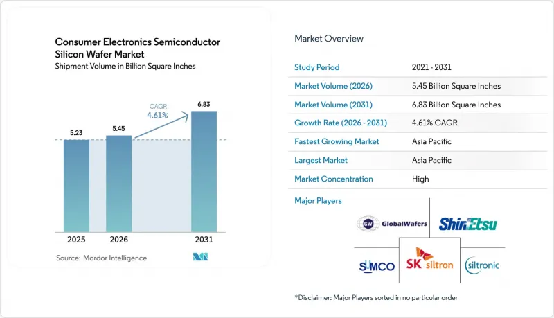
Strengthening demand for logic-intensive devices, migration to advanced node geometries, and government-backed fab incentives anchor this growth. Capital outlays by leading foundries continue to favor 300 mm substrates that maximize die counts, while specialty wafers such as silicon-on-insulator (SOI) gain share because they enable higher radio-frequency efficiency in 5G smartphones. Conversely, trailing-edge 200 mm capacity faces enduring margin pressure as analog and discrete devices remain on mature nodes. Regional diversification efforts in the United States and Europe are underway, yet Asia-Pacific retains its structural advantage in cost, existing supply chains, and installed wafer capacity.
Global Consumer Electronics Semiconductor Silicon Wafer Market Trends and Insights
Proliferation of 5G-Enabled Smartphones
Handset vendors embed multiple sub-6 GHz and millimeter-wave front-end modules, each containing discrete dies for low-noise and power amplifiers. Qualcomm's Snapdragon 8 Elite, fabricated on an advanced 4 nm process, allocates roughly 30% more wafer area per device than previous LTE platforms. Stand-alone 5G networks are rolling out in China and India, sustaining wafer pull-through even as global unit shipments plateau. Radio-frequency SOI substrates mitigate signal loss, enabling premium pricing that supports the 5.31% CAGR for SOI wafers. Partial substitution by gallium-nitride and indium-phosphide amplifiers tempers, but does not derail, incremental silicon demand.
Growth in High-Capacity Mobile Storage (3D NAND)
Smartphones equipped with 512 GB and 1 TB tiers accelerated a shift to 232-layer NAND stacks, increasing wafer starts and rework cycles. Reported shortages in late 2025 drove an earlier adoption of 1 Tb die schemes, raising silicon consumption per terabyte shipped. Concurrently, Samsung and SK hynix redirected 300 mm lines toward high-bandwidth memory, constricting consumer-grade NAND supply and lifting wafer average selling prices. The resulting demand spike peaks within two years as yield learning curves mature and new capacity comes online.
Capital-Intensive Large-Diameter Crystal Growth
A single 300 mm Czochralski line can exceed USD 400 million when factoring in pullers, slicing saws, and metrology. Equipment lead times often surpass two years, delaying new capacity during cyclical upswings. Siltronic's mid-single-digit revenue decline outlook for 2026 underscores how prolonged inventory digestion and deferred capex amplify fixed-cost exposure. SUMCO's planned closure of its Miyazaki 200 mm plant by the end of 2026 reflects legacy overcapacity and the capital burden of retooling. Higher labor and energy costs in North America and Europe further elevate breakeven thresholds, tightening this restraint.
Other drivers and restraints analyzed in the detailed report include:
- Expansion of Consumer IoT and Wearables
- Government Incentives for Domestic Logic Fabs
- Carbon-Footprint Caps from Consumer OEMs
For complete list of drivers and restraints, kindly check the Table Of Contents.
Segment Analysis
The 300 mm class captured 71.29% of the consumer electronics semiconductor silicon wafer market share in 2025, reflecting superior die-per-wafer economics that outweigh higher tool costs. This segment follows a growth curve aligned with the overall 4.61% CAGR as foundries channel record capex toward 3 nm and gate-all-around nodes. TSMC alone earmarked USD 52-56 billion for 2026 expansions, nearly all of which were devoted to 300 mm fabs. The consumer electronics semiconductor silicon wafer market size for 300 mm platforms is poised to reach 4,900 million square inches by 2031.
Emerging thinning and bonding techniques enable 300 mm substrates below 50 µm, unlocking applications once restricted to smaller diameters. Meanwhile, 200 mm lines persist for analog, MEMS, and power discretes, where process migration delivers limited benefit. Sub-150-mm wafers are receding to niche roles, chiefly high-resistivity RF switches and specialty sensors. Supply rationalization, including SUMCO's Miyazaki shutdown, helps stabilize pricing for legacy nodes even as premium 300 mm output scales.
The Consumer Electronics Semiconductor Silicon Wafer Market Report is Segmented by Wafer Diameter (Up To 150 Mm, 200 Mm, 300 Mm), Semiconductor Device Type (Logic, Memory, and More), Wafer Type (Prime Polished, Epitaxial, Specialty Silicon, and More), and Geography (North America, Europe, Asia-Pacific, South America, Middle East, Africa). The Market Forecasts are Provided in Terms of Shipment Volume (Square Inches).
Geography Analysis
Asia-Pacific led the consumer electronics semiconductor silicon wafer market share with 84.78% of 2025 volume and is advancing at a 5.78% CAGR through 2031. The region benefits from deep supply chains in Taiwan, South Korea, Japan, and China, each supported by multi-billion-dollar incentives for advanced logic fabs. TSMC's heavy 2026 capital program and China's goal of holding one-quarter of global 12-inch capacity further anchor demand. South Korean firms are pivoting 300 mm lines to high-bandwidth memory, tightening local supply for commodity NAND. India's USD 10 billion semiconductor mission brings new proposals, yet wafer production there still relies on imports.
North America is growing from a low base as the CHIPS and Science Act channels USD 36.4 billion into fab construction. TSMC's Arizona complex and Intel's Ohio project will stimulate local substrate pull once high-volume manufacturing begins in 2027. GlobalWafers plans the first U.S. 300 mm wafer plant in two decades, but higher labor and power costs temper its cost position. Europe mobilized EUR 80 billion under the EU Chips Act, focusing on analog and power devices in Germany and France. Siltronic's revenue outlook points to continued inventory digestion, yet regional funding should slow the talent drain to Asia.
South America, the Middle East, and Africa together account for only a sliver of the consumer electronics semiconductor silicon wafer market size because they lack large crystal-growth facilities. These regions depend on imports from Asia and, to a lesser extent, Europe and the United States. Global ISO 9001 and ISO 14001 standards maintain product quality consistency, but geographic concentration still exposes the supply chain to natural disasters and geopolitical tensions.
- Shin-Etsu Chemical Co., Ltd.
- SUMCO Corporation
- GlobalWafers Co., Ltd.
- Siltronic AG
- SK siltron Co., Ltd.
- Soitec S.A.
- National Silicon Industry Group Co., Ltd.
- Wafer Works Corp.
- Okmetic Oy
- Ferrotec Holdings Corporation
- Hebei Puxing Electronic Technology Co., Ltd.
- Zhonghuan Semiconductor Co., Ltd.
- Hangzhou Semiconductor Wafer Co., Ltd.
- GRINM Semiconductor Materials Co., Ltd.
- MCL Electronic Materials Co., Ltd.
- Shanghai Simgui Technology Co., Ltd.
- Virginia Semiconductor, Inc.
- Silicon Valley Microelectronics, Inc.
- Topsil Semiconductor Materials A/S
- Silicon Materials, Inc.
Additional Benefits:
- The market estimate (ME) sheet in Excel format
- 3 months of analyst support
TABLE OF CONTENTS
1 INTRODUCTION
- 1.1 Study Assumptions and Market Definition
- 1.2 Scope of the Study
2 RESEARCH METHODOLOGY
3 EXECUTIVE SUMMARY
4 MARKET LANDSCAPE
- 4.1 Market Overview
- 4.2 Market Drivers
- 4.2.1 Proliferation of 5G-Enabled Smartphones
- 4.2.2 Growth in High-Capacity Mobile Storage (3D NAND)
- 4.2.3 Expansion of Consumer IoT and Wearables
- 4.2.4 Government Incentives for Domestic Logic Fabs
- 4.2.5 Adoption of TSV Interposers in AR/VR Headsets
- 4.2.6 Silicon Photonics Uptake in XR Devices
- 4.3 Market Restraints
- 4.3.1 Capital-Intensive Large-Diameter Crystal Growth
- 4.3.2 Supply Constraints of High-Purity Polysilicon
- 4.3.3 Shift of RF Modules to Compound Substrates
- 4.3.4 Carbon-Footprint Caps from Consumer OEMs
- 4.4 Industry Value Chain Analysis
- 4.5 Regulatory Landscape
- 4.6 Technology Analysis
- 4.7 Impact of Macroeconomic Factors on the Market
- 4.8 Porter's Five Forces Analysis
- 4.8.1 Bargaining Power of Suppliers
- 4.8.2 Bargaining Power of Buyers
- 4.8.3 Threat of New Entrants
- 4.8.4 Threat of Substitutes
- 4.8.5 Intensity of Competitive Rivalry
5 MARKET SIZE AND GROWTH FORECASTS (VOLUME)
- 5.1 By Wafer Diameter
- 5.1.1 Up to 150 mm
- 5.1.2 200 mm
- 5.1.3 300 mm
- 5.2 By Semiconductor Device Type
- 5.2.1 Logic
- 5.2.2 Memory
- 5.2.3 Analog
- 5.2.4 Discrete
- 5.2.5 Other Semiconductor Device Types (Optoelectronics, Sensors, Micro)
- 5.3 By Wafer Type
- 5.3.1 Prime Polished
- 5.3.2 Epitaxial
- 5.3.3 Silicon-on-Insulator (SOI)
- 5.3.4 Specialty Silicon (High-Resistivity, Power, Sensor-Grade)
- 5.4 By Geography
- 5.4.1 North America
- 5.4.1.1 United States
- 5.4.1.2 Canada
- 5.4.1.3 Mexico
- 5.4.2 Europe
- 5.4.2.1 Germany
- 5.4.2.2 United Kingdom
- 5.4.2.3 France
- 5.4.2.4 Rest of Europe
- 5.4.3 Asia-Pacific
- 5.4.3.1 China
- 5.4.3.2 Japan
- 5.4.3.3 India
- 5.4.3.4 South Korea
- 5.4.3.5 Taiwan
- 5.4.3.6 Rest of Asia-Pacific
- 5.4.4 South America
- 5.4.5 Middle East
- 5.4.6 Africa
- 5.4.1 North America
6 COMPETITIVE LANDSCAPE
- 6.1 Market Concentration
- 6.2 Strategic Moves
- 6.3 Market Share Analysis
- 6.4 Company Profiles (includes Global Level Overview, Market Level Overview, Core Segments, Financials as available, Strategic Information, Market Rank/Share, Products and Services, Recent Developments)
- 6.4.1 Shin-Etsu Chemical Co., Ltd.
- 6.4.2 SUMCO Corporation
- 6.4.3 GlobalWafers Co., Ltd.
- 6.4.4 Siltronic AG
- 6.4.5 SK siltron Co., Ltd.
- 6.4.6 Soitec S.A.
- 6.4.7 National Silicon Industry Group Co., Ltd.
- 6.4.8 Wafer Works Corp.
- 6.4.9 Okmetic Oy
- 6.4.10 Ferrotec Holdings Corporation
- 6.4.11 Hebei Puxing Electronic Technology Co., Ltd.
- 6.4.12 Zhonghuan Semiconductor Co., Ltd.
- 6.4.13 Hangzhou Semiconductor Wafer Co., Ltd.
- 6.4.14 GRINM Semiconductor Materials Co., Ltd.
- 6.4.15 MCL Electronic Materials Co., Ltd.
- 6.4.16 Shanghai Simgui Technology Co., Ltd.
- 6.4.17 Virginia Semiconductor, Inc.
- 6.4.18 Silicon Valley Microelectronics, Inc.
- 6.4.19 Topsil Semiconductor Materials A/S
- 6.4.20 Silicon Materials, Inc.
7 MARKET OPPORTUNITIES AND FUTURE OUTLOOK
- 7.1 White-Space and Unmet-Need Assessment
