
|
시장보고서
상품코드
2062307
프로필러미터 시장 : 시장 점유율 분석, 업계 동향 및 통계, 성장 예측(2026-2031년)Profilometer - Market Share Analysis, Industry Trends & Statistics, Growth Forecasts (2026 - 2031) |
||||||
 Mordor Intelligence
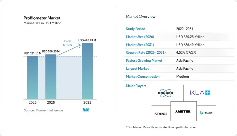
프로필러미터 시장 규모는 2025년 5억 2,515만 달러로 평가되었고, 2026년에는 5억 5,025만 달러로 추정되고, 2031년까지 6억 8,649만 달러에 이를 것으로 예측되며, 2026-2031년 CAGR 4.52%로 성장할 전망입니다.
본 보고서는 기술별(접촉식 스타일러스 프로파일 측정기, 백색광 간섭법 프로파일 측정기 등), 측정 차원별(2차원 프로파일 측정 등), 폼 팩터별(벤치탑 및 실험실 시스템, 인라인 및 온머신 시스템, 휴대용 및 핸드헬드 시스템), 최종 이용 산업별(반도체 및 전자, 자동차, 기타), 지역별로 분류되어 있습니다. 시장 전망은 금액(달러) 기준으로 제시되어 있습니다.
세계의 프로필러미터 시장 동향 및 인사이트
반도체 제조 분야에서 정밀 표면 특성 평가에 대한 수요 증가
2nm 이하의 로직 노드 및 하이브리드 본딩 상호 연결에서는 보이드 및 임계 전압의 변동을 억제하기 위해 팹은 웨이퍼의 표면 거칠기를 0.3nm Rq 이하로 제어해야 합니다. 2025년 생산 능력 확대에 따라 대만과 한국에 도입된 인라인 백색광 간섭계를 통해 스크랩이 15% 감소했으며, 폐루프 CMP 제어 분야에서 프로필러미터의 가치 제안이 입증되었습니다. 위상 변이 알고리즘, 격리 테이블 및 추적 가능한 ISO 25178-604 교정용 기준편을 통해 300mm 웨이퍼 전체에 걸쳐 옹스트롬 수준의 재현성을 실현함으로써, 파운드리 감사 요건을 충족하고 벤더 종속성을 강화하고 있습니다.
비접촉 및 3D 프로파일 측정 기술로의 전환
광학식 프로파일 측정은 연질 코팅이나 취약한 나노 구조에서 스타일러스로 인한 변형을 배제합니다. Sensofar사의 멀티 센서 ‘S Neox Five Axis’ 플랫폼을 통해 사용자는 스캔 중에 공초점, 초점 변동, 간섭계 모드를 전환할 수 있으며, 이를 통해 항공우주용 터빈 블레이드의 검사 시간을 40% 단축하고 있습니다(2). NIST의 적층 가공에 관한 연구에 따르면, 챔버 내 공초점 센서를 통해 제조 과정을 중단하지 않고도 각 파우더 베드 층을 10µm의 해상도로 매핑할 수 있으며, 이를 통해 레이저 출력을 실시간으로 보정할 수 있음이 입증되었습니다.
첨단 3D 광학 시스템에 대한 고액의 설비 투자
자동 스티칭 기능을 갖춘 조사용 간섭계는 30만 달러 이상이나 하기 때문에 특히 중소기업(SME)의 경우 도입에 큰 장벽이 되고 있습니다. 이러한 막대한 비용 때문에 명확하고 측정 가능한 수익이 없는 한 중소기업이 투자를 정당화하기 어려운 경우가 많습니다. 폴리테크사의 Pro.Surf+는 이 문제의 전형적인 예입니다. 이러한 조직의 조달 위원회는 막대한 지출을 승인하기 전에, 특히 정량화 가능한 불량품 감축으로 이어지는 상세한 투자 수익률(ROI) 분석을 자주 요구합니다. 이러한 재무적 면에 대한 면밀한 검토는 잠재적인 이점이 있음에도 불구하고, 중소기업이 첨단 측정 솔루션을 도입할 때 직면하는 어려움을 여실히 드러내고 있습니다.
부문별 분석
2025년 매출액 중 백색광 간섭법이 41.75%를 차지했으며, TSV의 깊이와 MEMS의 단차에서 서브나노미터급 정밀도를 실현함으로써 프로필러미터 시장에 기여했습니다. 제조업체들이 생산 라인 환경에서 경사가 많은 다층 구조에 대응하는 검사를 요구하는 가운데, 색 분산형 공초점 및 프린지 투영 솔루션은 2031년까지 연평균 5.23%의 성장률을 기록하며 시장 평균을 상회할 것으로 전망됩니다. 간섭법 측정기인 프로필러미터 시장 규모는 2031년까지 2억 7,000만 달러로 확대될 것으로 예상되는 반면, 공초점 하위 부문은 1억 8,500만 달러에 달하며, 기존 장비를 교체하지 않고도 그 격차를 좁혀갈 전망입니다.
Zygo사와 키엔스사의 2세대 멀티 센서 헤드는 간섭법, 공초점 현미경, 초점 변동 등의 첨단 기술을 하나의 소형 패키지에 통합하고 있습니다. 이번 통합을 통해 대규모 교육의 필요성이 대폭 줄어들게 되며, 다품종 생산을 수행하는 제조 시설이 통합된 플랫폼에서 운영을 도입하고 표준화할 수 있게 됩니다. 또한, 이러한 표준화로 인해 고객의 전환 비용이 증가하게 되며, 이는 프로필러미터 시장에서 공급업체의 이익률을 유지 및 향상시키는 데 중요한 요인이 됩니다.
3차원 표면 측정 시스템은 2025년에 58.31%의 시장 점유율을 차지하며, 연평균 5.11%의 성장률을 보이고 있습니다. 이는 ISO 25178에 따른 세계 표준화와 Sa, Svk, 피크 재료 부피와 같은 측정 지표의 통계적 견고성을 반영한 것입니다. 자동차용 호닝, 정형외과용 임플란트의 텍스처링, 전기차용 배터리 전극 등 각 분야에서는 모두 표면 측정 규격이 채택되고 있으며, 이에 따라 프로필러미터 시장 점유율이 2차원 스타일러스 트레이싱에서 전환되는 추세가 가속화되고 있습니다. 2차원 프로필러미터는 고처리량의 합격·불합격 판정 분야에서 여전히 확고한 입지를 유지하고 있지만, 2026-2028년 신규 설비 투자의 대부분은 면 측정 지원 플랫폼에 집중되고 있습니다.
클라우드 기반 GPU 분석을 통해 1,000만 개의 고도 지도가 불과 몇 초 만에 처리되게 되어, 실시간 의사결정 루프가 가능해졌으며, 원활한 원격 협업이 촉진되고 있습니다. 이러한 기술적 진보에 힘입어, 시장 수요는 하드웨어 솔루션에만 초점을 맞추는 벤더에서 견고한 소프트웨어 생태계를 제공하는 벤더로 이동하고 있습니다. 이러한 변화로 인해 프로파일 미터 시장 진입 장벽은 더욱 높아졌으며, 신규 진출기업이 입지를 다지기란 점점 더 어려워지고 있습니다.
지역별 분석
아시아태평양은 2025년 매출의 37.53%를 차지했으며, CMP 및 하이브리드 본딩 제어용 프로필러미터를 도입하는 대만과 한국의 주조 시설 확장에 따른 500억 달러 규모의 투자에 힘입어 2031년까지 연평균 성장률(CAGR) 4.38%를 나타낼 것으로 예측됩니다. 중국 본토에서는 국가 IC 기금이 지원하는 150억 달러 규모의 계측 기술 지원 정책이 국내 간섭계 도입을 촉진하고 있지만, 최고 해상도 측면에서는 여전히 기존 제조업체들에 미치지 못하는 상황입니다. 인도의 PLI(생산 연계형 인센티브) 전자기기 제도에서는 ISO 17025 인증 실험실의 설치를 의무화하고 있어, 벵갈루루와 푸네 전역에서 프로파일 미터에 대한 수요를 끌어올리고 있습니다.
북미는 2025년 수요의 약 28%를 차지했으며, 520억 달러 규모의 미국 CHIPS 법안과 보잉·에어버스 양사의 항공우주 공급망에 힘입고 있습니다. 인텔, 마이크론, 전 세계 파운드리 업체들은 2027년까지 팹을 개설할 계획이며, 수율을 확보하고 중기적인 성장의 기반을 마련하기 위해 인라인 프로파일러 제품군을 도입할 예정입니다. 캐나다 퀘벡주에 위치한 항공우주 허브에서는 기체 상에서 검사를 수행하기 위해 휴대용 프로파일 측정기가 널리 사용되고 있습니다. 한편, 멕시코에서는 전기차 구동계 열풍에 힘입어 1차 공급업체들의 구매가 활성화되고 있습니다.
유럽은 2025년 매출의 약 25%를 차지했으며, 독일은 배터리 전극의 표면 질감을 규정하는 전기차 생산 라인에 100억 유로(113억 달러)를 투자하고, 프랑스의 항공우주 클러스터는 NADCAP 표면 감사를 실시하고 있으며, EU 칩 법은 계측 장비를 많이 사용하는 반도체 팹에 430억 유로(486억 달러)를 투입하고 있습니다. DIN EN ISO 21920, AMS2700, SEMI M59와 같은 표준 규격의 파편화로 인해 유럽 전역에서의 조달은 복잡해지고 있지만, 2024년에 최종 확정된 ISO 10360 광학 수락 시험이 공통된 검증 기준을 제공함으로써 유럽 대륙 전체에서의 채택을 뒷받침하고 있습니다.
기타 혜택 :
- 엑셀 형식 시장 예측(ME) 시트
- 3개월간의 애널리스트 지원
자주 묻는 질문
목차
제1장 서론
제2장 조사 방법
제3장 주요 요약
제4장 시장 구도
제5장 시장 규모 및 성장 예측
제6장 경쟁 구도
제7장 시장 기회 및 향후 전망
AJY 26.06.26According to Mordor Intelligence, the profilometer market size is expected to increase from USD 525.15 million in 2025 to USD 550.25 million in 2026 and reach USD 686.49 million by 2031, growing at a CAGR of 4.52% over 2026-2031.
This report is Segmented by Technology (Contact-Stylus Profilometers, White-Light Interferometry Profilometers, and More), Measurement Dimension (2-D Profilometry, and More), Form Factor (Benchtop/Lab Systems, In-Line/On-Machine Systems, and Portable/Hand-Held Systems), End-Use Industry (Semiconductor and Electronics, Automotive, and More), and Geography. The Market Forecasts are Provided in Terms of Value (USD).
Global Profilometer Market Trends and Insights
Rising Demand for Precision Surface Characterization in Semiconductor Manufacturing
Sub-2 nm logic nodes and hybrid-bonding interconnects require fabs to control wafer roughness to below 0.3 nm Rq to suppress voids and threshold-voltage shifts. Inline white-light interferometers installed in Taiwan and South Korea during 2025 capacity expansions have cut scrap by 15%, validating the profilometer market's value proposition for closed-loop CMP control. Phase-shifting algorithms, isolation tables, and traceable ISO 25178-604 calibration artifacts allow angstrom-level repeatability across 300 mm wafers, satisfying foundry audit requirements and reinforcing vendor lock-in.
Shift Toward Non-Contact and 3D Profilometry Technologies
Optical profilometry eliminates stylus-induced deformation on soft coatings and fragile nanostructures. Sensofar's multi-sensor S Neox Five Axis platform lets users toggle among confocal, focus-variation, and interferometry modes mid-scan, reducing inspection time 40% for aerospace turbine blades[2].NIST's additive-manufacturing study proved in-chamber confocal sensors can map each powder-bed layer at 10 µm resolution without pausing the build, enabling real-time laser-power corrections.
High Capital Expenditure of Advanced 3D Optical Systems
Research-grade interferometers with automated stitching cost over USD 300,000, creating a significant barrier to adoption, particularly for small and medium-sized enterprises (SMEs). This high cost often makes it difficult for SMEs to justify the investment without clear, measurable returns. Polytec's Pro.Surf+ serves as a prime example of this issue. Procurement committees within these organizations frequently require a detailed return on investment (ROI) analysis, specifically tied to quantifiable scrap savings, before approving such substantial expenditures. This financial scrutiny highlights the difficulty SMEs face in adopting advanced metrology solutions despite their potential benefits.
Other drivers and restraints analyzed in the detailed report include:
- Quality Control and Surface Inspection Needs Across Diverse End-Use Industries
- Integration With Automation and Smart Manufacturing
- Competing Surface-Metrology Technologies Cannibalizing Share
For complete list of drivers and restraints, kindly check the Table Of Contents.
Segment Analysis
White-light interferometry accounted for 41.75% of 2025 revenue, benefiting the profilometer market through its sub-nm accuracy across TSV depths and MEMS steps. Chromatic confocal and fringe-projection solutions will outpace the market at 5.23% annually through 2031 as manufacturers seek slope-rich, multilayer-friendly inspection in line environments. The profilometer market size for interferometry instruments is projected to expand to USD 270 million by 2031, whereas confocal sub-segments will climb to USD 185 million, narrowing the gap without displacing legacy installs.
Second-generation multi-sensor heads from Zygo and Keyence integrate advanced technologies such as interferometry, confocal microscopy, and focus variation into a single, compact package. This integration significantly reduces the need for extensive training, enabling high-mix manufacturing facilities to adopt and standardize operations on a unified platform. Additionally, this standardization increases switching costs for customers, a critical factor in maintaining and enhancing vendor profit margins in the profilometer market.
Three-dimensional areal systems held a 58.31% share in 2025 and are growing at 5.11% annually, reflecting ISO 25178's global harmonization and the statistical robustness of Sa, Svk, and peak-material-volume metrics. Automotive honing, orthopedic implant texturing, and EV battery electrodes all cite areal standards, accelerating the migration of profilometer market share away from two-dimensional stylus traces. Two-dimensional profilometers retain a foothold in high-throughput go/no-go checks, yet most new capex in 2026-2028 is directed toward areal-capable platforms.
Cloud-based GPU analytics now process 10-million-point height maps in mere seconds, enabling real-time decision-making loops and facilitating seamless remote collaboration. This technological advancement has shifted market demand toward vendors offering robust software ecosystems rather than those focusing solely on hardware solutions. This shift has further strengthened the barriers to entry in the profilometer market, making it increasingly challenging for new competitors to establish a foothold.
Geography Analysis
Asia-Pacific accounted for 37.53% of 2025 revenue and will log a 4.38% CAGR to 2031, buoyed by USD 50 billion in Taiwanese and South Korean foundry expansions that embed profilometers for CMP and hybrid-bond bonding control. Mainland China's USD 15 billion metrology stimulus under its National IC Fund catalyzes domestic interferometer builds, though top-tier resolution still trails incumbents. India's PLI electronics scheme mandates ISO 17025 labs, boosting demand for profilometers across Bengaluru and Pune.
North America accounted for ~28% of 2025 demand, backed by the USD 52 billion U.S. CHIPS Act and the Boeing-Airbus aerospace supply chains. Intel, Micron, and GlobalFoundries plan to open fabs through 2027, with inline profilometer suites to ensure yield and anchor mid-term growth. Canada's Quebec aerospace hub prefers portable profilometers for on-wing inspection, while Mexico's EV drivetrain boom drives purchases among Tier 1 suppliers.
Europe held roughly 25% of 2025 sales, with Germany investing EUR 10 billion (USD 11.3 billion) in EV lines that specify battery-electrode areal texture, France's aerospace cluster enforcing NADCAP surface audits, and the EU Chips Act channeling EUR 43 billion (USD 48.6 billion) into metrology-rich semiconductor fabs. Fragmented standards, DIN EN ISO 21920, AMS2700, SEMI M59, complicate pan-European procurement, but ISO 10360 optical acceptance tests finalized in 2024 now provide common verification tracks, aiding continental adoption.
- Bruker Corporation
- KLA Corporation
- Keyence Corporation
- GBS Metrology GmbH
- AMETEK Inc.
- Mahr GmbH
- Mitutoyo Corporation
- Hexagon AB
- Jenoptik AG
- Park Systems Corporation
- Sensofar Tech SL
- Nanovea Inc.
- HORIBA Group
- Polytec GmbH
- Milexia Group
- Paragon Instruments
- Intertek Group plc
- Zygo Corporation
- Trimos SA
- Veeco Instruments Inc.
Additional Benefits:
- The market estimate (ME) sheet in Excel format
- 3 months of analyst support
TABLE OF CONTENTS
1 INTRODUCTION
- 1.1 Study Assumptions and Market Definition
- 1.2 Scope of the Study
2 RESEARCH METHODOLOGY
3 EXECUTIVE SUMMARY
4 MARKET LANDSCAPE
- 4.1 Market Overview
- 4.2 Market Drivers
- 4.2.1 Rising Demand for Precision Surface Characterization in Semiconductor Manufacturing
- 4.2.2 Quality Control and Surface Inspection Needs Across Diverse End-Use Industries
- 4.2.3 Shift Toward Non-Contact and 3D Profilometry Technologies
- 4.2.4 Integration With Automation and Smart Manufacturing
- 4.2.5 Adoption of Profilometers for In-Situ Monitoring in Additive Manufacturing Processes
- 4.2.6 Emerging Demand for Surface Metrology in Quantum Computing Hardware Fabrication
- 4.3 Market Restraints
- 4.3.1 High Capital Expenditure of Advanced 3D Optical Systems
- 4.3.2 Competing Surface-Metrology Technologies Cannibalizing Share
- 4.3.3 Limited Standardization of Areal Texture Parameters Across Industries
- 4.3.4 Dependency on Rare-Earth Optical Components With Volatile Supply Chains
- 4.4 Industry Supply-Chain Analysis
- 4.5 Impact of Macroeconomic Factors on the Market
- 4.6 Regulatory Landscape
- 4.7 Technological Outlook
- 4.8 Porter's Five Forces Analysis
- 4.8.1 Threat of New Entrants
- 4.8.2 Bargaining Power of Suppliers
- 4.8.3 Bargaining Power of Buyers
- 4.8.4 Threat of Substitutes
- 4.8.5 Competitive Rivalry
5 MARKET SIZE AND GROWTH FORECASTS (VALUE)
- 5.1 By Technology
- 5.1.1 Contact-Stylus Profilometers
- 5.1.2 White-Light Interferometry Profilometers
- 5.1.3 Confocal Laser-Scanning Profilometers
- 5.1.4 Chromatic Confocal and Fringe-Projection Profilometers
- 5.2 By Measurement Dimension
- 5.2.1 2-D Profilometry
- 5.2.2 3-D Areal Profilometry
- 5.3 By Form Factor
- 5.3.1 Benchtop/Lab Systems
- 5.3.2 In-Line/On-Machine Systems
- 5.3.3 Portable/Hand-Held Systems
- 5.4 By End-Use Industry
- 5.4.1 Semiconductor and Electronics
- 5.4.2 Automotive
- 5.4.3 Aerospace and Defence
- 5.4.4 Healthcare
- 5.4.5 Manufacturing
- 5.4.6 Energy and Power
- 5.5 By Geography
- 5.5.1 North America
- 5.5.1.1 United States
- 5.5.1.2 Canada
- 5.5.1.3 Mexico
- 5.5.2 Europe
- 5.5.2.1 United Kingdom
- 5.5.2.2 Germany
- 5.5.2.3 France
- 5.5.2.4 Italy
- 5.5.2.5 Rest of Europe
- 5.5.3 Asia-Pacific
- 5.5.3.1 China
- 5.5.3.2 Japan
- 5.5.3.3 India
- 5.5.3.4 Rest of Asia-Pacific
- 5.5.4 South America
- 5.5.4.1 Brazil
- 5.5.4.2 Rest of South America
- 5.5.5 Middle East
- 5.5.5.1 Saudi Arabia
- 5.5.5.2 United Arab Emirates
- 5.5.5.3 Rest of Middle East
- 5.5.6 Africa
- 5.5.6.1 South Africa
- 5.5.6.2 Nigeria
- 5.5.6.3 Rest of Africa
- 5.5.1 North America
6 COMPETITIVE LANDSCAPE
- 6.1 Market-Share Analysis
- 6.2 Company Profiles (includes Global Level Overview, Market Level Overview, Core Segments, Financials as available, Strategic Information, Market Rank/Share, Products and Services, Recent Developments)
- 6.2.1 Bruker Corporation
- 6.2.2 KLA Corporation
- 6.2.3 Keyence Corporation
- 6.2.4 GBS Metrology GmbH
- 6.2.5 AMETEK Inc.
- 6.2.6 Mahr GmbH
- 6.2.7 Mitutoyo Corporation
- 6.2.8 Hexagon AB
- 6.2.9 Jenoptik AG
- 6.2.10 Park Systems Corporation
- 6.2.11 Sensofar Tech SL
- 6.2.12 Nanovea Inc.
- 6.2.13 HORIBA Group
- 6.2.14 Polytec GmbH
- 6.2.15 Milexia Group
- 6.2.16 Paragon Instruments
- 6.2.17 Intertek Group plc
- 6.2.18 Zygo Corporation
- 6.2.19 Trimos SA
- 6.2.20 Veeco Instruments Inc.
7 MARKET OPPORTUNITIES AND FUTURE OUTLOOK
- 7.1 White-Space and Unmet-Need Assessment