
|
시장보고서
상품코드
2063294
질화갈륨(GaN) 기판 : 시장 점유율 분석, 업계 동향 및 통계, 성장 예측(2026-2031년)GaN Substrate - Market Share Analysis, Industry Trends & Statistics, Growth Forecasts (2026 - 2031) |
||||||
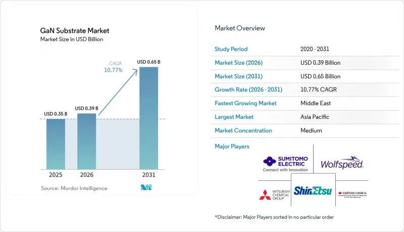
Mordor Intelligence에 의하면, 질화갈륨(GaN) 기판 시장 규모는 2025년 3억 5,000만 달러로 평가되었습니다. 2026년 3억 9,000만 달러로 확대되어 2031년까지 6억 5,000만 달러에 이를 것으로 예상되며 2026년부터 2031년에 걸쳐 CAGR은 10.77%를 나타낼 전망입니다.
본 보고서는 기판 유형(GaN-On-Sapphire, GaN-On-Silicon, GaN-On-Silicon Carbide, Native GaN(GaN-On-GaN), GaN-On-Diamond), 웨이퍼 크기(2인치, 4인치, 6인치, 기타), 용도(레이저 다이오드, 고주파 소자 등), 최종 이용 산업(소비자용 전자기기, 자동차 및 운송기기 등), 지역별로 분류되어 있습니다. 시장 전망은 금액(달러) 기준으로 제시되어 있습니다.
세계의 질화갈륨(GaN) 기판 시장 동향 및 분석
전기차 급속 충전 시스템에서의 도입 확대
전기차 제조업체들은 현재 96%의 효율과 6 kW/L의 전력 밀도를 달성하는 GaN 기반 차량용 충전기를 사양으로 채택하고 있으며, 이 결과는 2025년 창안자동차가 Navitas사의 GaNSafe 장치를 도입했을 때 입증되었습니다. 그 후, Inovance Automotive사가 제공한 6.6 kW 유닛은 실리콘 IGBT에 비해 30% 더 높은 전력 밀도를 실현했으며, 충전기의 무게를 20% 줄였습니다. 인피니언의 자동차용 인증 완료된 100V GaN 트랜지스터는 2025년 하반기에 AEC-Q101 규격 인증을 획득함으로써, 인증 장벽을 극복했음이 확인되었습니다. 수요 곡선에 따르면, 2028년까지 연간 100만 대 이상의 GaN 충전기가 시장에 출시될 것으로 예상되며, 이러한 규모 수요는 기판 공급업체들이 6인치에서 8인치 플랫폼으로 전환하도록 촉진하는 요인이 될 것입니다. 따라서, 순수 GaN 및 GaN-on-SiC 공급업체들에게는 1차 자동차 시스템 통합사업자와 장기 공급 계약을 체결할 절호의 기회가 찾아왔습니다.
급증하는 Micro-LED 디스플레이 생산에 필요한, 결함이 적은 네이티브 GaN 웨이퍼
마이크로 LED 제조 공장에서는 불순물 밀도의 상한을 10⁴ cm-²로 정하고 있지만, 이 수준은 GaN-on-sapphire로는 달성할 수 없습니다. 현재, 암모니아 열법과 HVPE법을 결합한 성장 기술을 통해 이 임계값을 충족하는 자립형 GaN 웨이퍼를 제조할 수 있게 되었으며, 마이크로 LED 어레이를 CMOS 백플레인에 웨이퍼 단위로 일괄 전사하는 것이 가능해졌습니다. 미쓰비시 화학은 2025년, NEDO 프로그램의 일환으로 4인치 결정의 실증에 성공하여 월 1,000장의 생산을 목표로 하고 있습니다. 이를 통해 실외용 증강현실(AR) 헤드셋을 위해 10만 닛을 넘는 패널 밝기를 구현합니다. 각 디스플레이 제조업체들은 동시에 비방출 재결합을 억제하기 위한 측벽 패시베이션 기술을 개선하고 있으며, 기판의 품질이 최종적인 휘도 성능에 확실히 반영되도록 노력하고 있습니다.
Si나 SiC에 비해 높은 웨이퍼 가격 프리미엄이, 비용을 중시하는 부문에서의 채택을 제한하고 있습니다.
네이티브 GaN 및 GaN-on-SiC 웨이퍼는 여전히 6인치당 3,000-8,000달러 수준의 가격대를 유지하고 있으며, 이는 동급의 실리콘카바이드(SiC) 웨이퍼 가격의 5배에서 10배에 달할 전망입니다. 따라서民生용 및 산업용 설계자들은 비록 효율이 약간 떨어지더라도 고가의 부품 비용을 피하기 위해 실리콘 IGBT나 SiC MOSFET을 계속 사용하고 있습니다. 아모노열법(Amono-thermal)을 이용한 성장은 우수한 결정 품질을 제공하지만, 3,000바르의 오토클레이브를 수 주간 가동해야 하기 때문에 자본을 묶어두고 처리량을 제한하게 됩니다. 나고야 대학의 레이저를 이용한 웨이퍼 재사용 프로젝트에서는 소자의 성능을 저하시키지 않고 최대 10회까지 재활용이 가능함이 입증되었으나, 상업적인 사이클 타임은 아직 기존 파운드리 공정의 속도를 따라잡지 못하고 있습니다.
부문별 분석
GaN-on-silicon은 200mm 팹과의 원활한 호환성과 웨이퍼당 200달러 미만의 비용 덕분에 2025년 질화갈륨(GaN) 기판 시장 점유율의 31.19%를 차지했습니다. 인노사이언스(Innoscience)는 8인치 라인의 생산 능력을월13,000개 웨이퍼에서 2만 개 웨이퍼로 확대하고, 2030년까지 7만 개 웨이퍼를 목표로 하고 있으며, 중국의 생산 능력 면에서의 우위를 강조하고 있습니다. 다이아몬드 통합형 질화갈륨(GaN) 기판 시장 규모는 본딩 기술을 통해 열저항이 10 mm²K W-¹ 미만으로 감소하고, 위상 배열 레이더용으로 30 W mm-²를 초과하는 전력 밀도가 가능해짐에 따라, 2031년까지 연평균 성장률(CAGR) 11.24%로 확대될 것으로 전망됩니다.
기존의 GaN-on-sapphire는 일반 조명 분야에서 일정한 입지를 유지하고 있지만, 마이크로 LED 및 RF 부문이 결함 제어를 위해 네이티브 GaN으로 전환함에 따라 그 시장 점유율은 줄어들고 있습니다. GaN-on-SiC는 발열량이 많은 통신 및 방위 시스템에서 여전히 필수적인 요소로 자리 잡고 있으며, Qorvo와 Wolfspeed가 주요 공급업체로 활동하고 있습니다. 네이티브 GaN은 가격이 비싸지만, 수직형 파워 트랜지스터 및 파인 피치 디스플레이 백플레인용으로 극히 낮은 전위 수를 확보하고 있으며, 신에츠 화학공업의 300mm QST 복합 공정은 예측 기간 동안 비용과 품질 간의 격차를 해소할 가능성이 있습니다.
2025년에는 HVPE 리액터와 CMP 장비의 감가상각이 6인치 규격에서 완료됨에 따라, 6인치 기판 재고가 질화갈륨(GaN) 기판 시장 규모의 42.82%를 차지했습니다. 이러한 우위는 비용 효율성과 확장성을 실현한 6인치 제조 공정의 성숙도 덕분입니다. 스미토모 화학의 NEDO 지원 라인에서는 100-300µm/h의 성막 속도를 채택하여 사이클 타임의 경쟁력을 유지하는 한편, 결함 밀도를 105cm-² 미만으로 억제함으로써 다양한 용도에 적합한 고품질 기판을 확보하고 있습니다. 8인치 이상 부문은 인피니온의 300mm GaN 생산 라인 발표와 중국 내 IDM 기업들이 2030년까지월7만 장의 웨이퍼 생산을 계획하고 있는 점을 감안할 때, 2031년까지 연평균 성장률(CAGR) 11.51%를 나타낼 것으로 전망됩니다.
이러한 성장은 고출력·고주파 응용 분야에 대응하기 위한 대형 기판에 대한 수요 증가와 더불어, 제조 기술의 발전에 힘입어 이루어지고 있습니다. 2026년 초에는 8인치 독립형 GaN에 대한 개념 검증(PoC)이 이루어졌으나, 크래킹 및 CMP 시간 문제는 여전히 걸림돌로 남아 있어 양산 과정에서 해결해야 할 과제가 부각되고 있습니다. 2인치 및 4인치 웨이퍼는 여전히 연구 개발 및 틈새 RF 용도로 사용되고 있으며, 이러한 분야에서는 특수한 이용 사례에 소형 기판으로도 충분합니다. 한편, 300mm 복합 기판은 경제성이 향상되면 GaN을 주류 실리콘 팹에 도입하는 기반이 되어, 반도체 업계에서 더욱 광범위한 채택의 길을 열게 될 것입니다.
지역별 분석
2025년, 아시아·태평양 지역은 질화갈륨(GaN) 기판 시장 점유율의 41.33%를 차지했습니다. 중국의 IDM 기업들은 국내 설비 투자와 풍부한 갈륨 원료에 힘입어, 수요 증가에 대응하기 위해 8인치 GaN-on-silicon 생산 라인 확장을 계속하고 있습니다. 한편, 일본은 첨단 결정 성장 기술을 활용하여 프리 스탠딩형 네이티브 질화갈륨(GaN) 기판을 제조하고, 새로운 다이아몬드 본딩 기술 연구를 진행하고 있습니다. 한국의 디스플레이 제조업체들은 마이크로 LED 기술 로드맵을 추진하기 위해 네이티브 질화갈륨(GaN) 기판에 대한 의존도를 높이고 있으며, 인도의 AGNIT Semiconductors는 유리한 세제 혜택과 정부 지원 프로그램 하에서 생산을 확대되고 있습니다.
북미는 강력한 설계 리더십과 GaN-on-SiC 기판에 대한 방위 산업 분야 수요 증가를 결합하고 있습니다. 그러나 해당 지역은 국내 기판 생산 능력에 제약이 있어, 현재는 Kyma Technologies와 소규모 대학의 제조 시설로만 한정되어 있습니다. 유럽의 경쟁 우위는 벨기에의 Soitec EpiGaN 부문에 있으며, 이 회사는 해당 지역 전체의 질화갈륨(GaN) 기판 생산에서 매우 중요한 역할을 담당하고 있습니다. 또한, 유럽연합(EU)의 ‘칩법’은 광대역 갭 반도체 기술 분야의 자급자족 달성을 목표로 막대한 자금을 지원하고 있습니다.
중동은 가장 빠르게 성장하는 지역으로 부상하고 있으며, 2031년까지의 연평균 성장률(CAGR)은 11.33%로 예측됩니다. 이 지역의 정부계 펀드는 갈륨 비축을 적극적으로 추진하는 한편, 새로운 기판 제조 시설 설립에 자금을 지원하고 있습니다. 이러한 노력은 AI 데이터센터 및 국방 현대화 프로그램을 지원하는 광범위한 이니셔티브와 맥을 같이하고 있습니다. 남미와 아프리카는 아직 발전의 초기 단계에 있지만, 금세기 말까지 재생에너지 관련 GaN 수요를 창출할 잠재력을 지니고 있습니다. 이러한 성장은 현지 시장을 뒷받침하기 위한 지역적 생산 능력의 구축에 달려 있습니다.
기타 혜택 :
- 엑셀 형식 시장 예측(ME) 시트
- 3개월간의 애널리스트 지원
자주 묻는 질문
목차
제1장 서론
제2장 조사 방법
제3장 주요 요약
제4장 시장 구도
제5장 시장 규모 및 성장 예측
제6장 경쟁 구도
제7장 시장 기회 및 향후 전망
KTH 26.06.22According to Mordor Intelligence, the gaN substrate market size is expected to increase from USD 0.35 billion in 2025 to USD 0.39 billion in 2026 and reach USD 0.65 billion by 2031, growing at a CAGR of 10.77% over 2026-2031.

This report is Segmented by Substrate Type (GaN-On-Sapphire, GaN-On-Silicon, GaN-On-Silicon Carbide, Native GaN (GaN-On-GaN), and GaN-On-Diamond), Wafer Size (2 Inch, 4 Inch, 6 Inch, and More), Application (Laser Diodes, Radio-Frequency Devices, and More ), End-Use Industry (Consumer Electronics, Automotive and Transportation, and More), and Geography. Market Forecasts are Provided in Terms of Value (USD).
Global GaN Substrate Market Trends and Insights
Rising Adoption in EV On-Board Fast-Charging Systems
Electric-vehicle makers now specify GaN-based on-board chargers that hit 96% efficiency and 6 kW L-1 power density, results validated when Changan deployed Navitas GaNSafe devices in 2025. Subsequent 6.6 kW units from Inovance Automotive delivered 30% higher power density than silicon IGBTs and trimmed charger weight by 20%. Infineon's automotive-qualified 100 V GaN transistors cleared AEC-Q101 later in 2025, confirming that qualification hurdles have been overcome. Demand curves point to more than 1 million GaN chargers per year by 2028, a volume that motivates substrate suppliers to transition from 6-inch to 8-inch platforms. Native GaN and GaN-on-SiC suppliers, therefore, face a window to lock in long-term supply contracts with Tier-1 automotive integrators.
Surging Micro-LED Display Production Requiring Low-Defect Native GaN Wafers
Micro-LED fabs impose dislocation density ceilings of 104 cm-2, a level unreachable on GaN-on-sapphire. Hybrid ammonothermal and HVPE growth schemes now deliver free-standing GaN wafers that meet that threshold, enabling wafer-scale mass transfer of micro-LED arrays onto CMOS backplanes. Mitsubishi Chemical demonstrated 4-inch crystals under a NEDO program in 2025, aiming at 1 000 wafers per month and enabling panel luminance beyond 100 000 nits for outdoor augmented-reality headsets. Display houses are simultaneously refining sidewall passivation chemistries to keep non-radiative recombination in check, ensuring that substrate quality propagates to final brightness performance.
High Wafer Price Premium Versus Si and SiC Limiting Adoption in Cost-Sensitive Segments
Native GaN and GaN-on-SiC wafers still command USD 3 000-8 000 per 6-inch unit, five to ten times the tag on comparable silicon carbide wafers. Consumer and industrial designers therefore stick with silicon IGBTs or SiC MOSFETs, sacrificing modest efficiency gains to avoid heavy bill-of-materials penalties. Ammonothermal growth produces superb crystal quality but requires 3 000-bar autoclaves running for weeks, tying up capital and capping throughput. Laser-based wafer-reuse projects at Nagoya University demonstrate up to 10 recycles without degrading device metrics, yet commercial cycle times have not yet matched the cadence of conventional foundry flows.
Other drivers and restraints analyzed in the detailed report include:
- Telecom 5G/6G PA Build-Out Accelerating Demand for High-Thermal-Conductivity GaN-on-SiC Substrates
- Rapid Scale-Up of 6-Inch HVPE Free-Standing GaN Production Lowering Cost per cm2
- Device-Yield Losses from Threading-Dislocation Clusters on 6-Inch Wafers
For complete list of drivers and restraints, kindly check the Table Of Contents.
Segment Analysis
GaN-on-silicon held 31.19% of the GaN substrate market share in 2025, thanks to a seamless fit with 200 mm fabs and a sub-USD 200 cost per wafer. Innoscience ramped 8-inch lines from 13 000 to 20 000 wafers per month and targets 70 000 by 2030, underlining China's capacity lead. The GaN substrate market size for diamond-integrated variants is projected to grow at 11.24% CAGR through 2031 as bonding lowers thermal resistance below 10 mm2 K W-1 and enables power densities above 30 W mm-2 for phased-array radar.
Legacy GaN-on-sapphire maintains a foothold in general lighting, but share erodes as micro-LED and RF segments pivot to native GaN for defect control. GaN-on-SiC stays indispensable for high-heat telecom and defense systems, with Qorvo and Wolfspeed the default suppliers. Native GaN, though pricier, secures ultra-low dislocation counts for vertical power transistors and fine-pitch display backplanes, and Shin-Etsu's 300 mm QST composite route may bridge cost and quality gaps over the forecast horizon.
Six-inch inventory represented 42.82% of the GaN substrate market size in 2025 as HVPE reactors and CMP tools are fully depreciated at that diameter. This dominance is attributed to the maturity of six-inch manufacturing processes, which have achieved cost efficiency and scalability. Sumitomo Chemical's NEDO-backed line uses 100-300 µm h-1 deposition rates to keep cycle times competitive and pull defect density below 105 cm-2, ensuring high-quality substrates suitable for various applications. The 8-inch-and-above cohort is on track for 11.51% CAGR to 2031, catalyzed by Infineon's announcement of 300 mm GaN lines and Chinese IDMs mapping 70 000 wafers per month by 2030.
This growth is driven by increasing demand for larger substrates to support high-power, high-frequency applications, as well as advancements in manufacturing technologies. A proof-of-concept 8-inch free-standing GaN was demonstrated in early 2026, yet cracking and CMP time remain stumbling blocks, highlighting the challenges in scaling up production. Two- and four-inch wafers persist in R&D and niche RF applications, where smaller substrates are sufficient for specialized use cases. Meanwhile, 300 mm composite substrates position GaN for mainstream silicon fabs once economics tighten, paving the way for broader adoption in the semiconductor industry.
Geography Analysis
Asia-Pacific accounted for 41.33% of the GaN substrate market share in 2025. Chinese IDMs, supported by domestic capital investments and abundant gallium feedstock, continue to expand their 8-inch GaN-on-silicon production lines to meet growing demand. Japan, on the other hand, capitalizes on its advanced crystal growth expertise to produce free-standing native GaN substrates and to explore emerging diamond-bonded technologies. South Korea's display manufacturers are increasingly relying on native GaN substrates to advance their micro-LED technology roadmaps, while India's AGNIT Semiconductors is scaling up production under favorable tax incentives and government support programs.
North America combines its strong design leadership with increasing defense-related demand for GaN-on-SiC substrates. However, the region faces limitations in domestic substrate production capacity, currently limited to Kyma Technologies and small-scale university fabrication facilities. Europe's competitive edge lies in Belgium's Soitec EpiGaN unit, which plays a pivotal role in GaN substrate production across the region. Additionally, the European Union Chips Act provides significant funding aimed at achieving self-sufficiency in wide-bandgap semiconductor technologies.
The Middle East is emerging as the fastest-growing region, with a projected CAGR of 11.33% through 2031. Sovereign wealth funds in the region are actively stockpiling gallium and financing the establishment of greenfield substrate fabrication facilities. These efforts align with broader initiatives to support AI data centers and defense modernization programs. South America and Africa, while still in the early stages of development, hold potential for unlocking renewable energy-related GaN demand by the end of the decade. This growth is contingent on the establishment of regional fabrication capabilities to support local markets.
- Sumitomo Electric Industries, Ltd.
- Mitsubishi Chemical Corporation
- Wolfspeed, Inc.
- Shin-Etsu Chemical Co., Ltd.
- SCIOCS Company, Ltd.
- Kyma Technologies, Inc.
- Suzhou Nanowin Science and Technology Co., Ltd.
- PAM-Xiamen Powerway Advanced Material Co., Ltd.
- Advanced Engineering Materials Limited
- Dowa Electronics Materials Co., Ltd.
- Nitride Semiconductors Co., Ltd.
- EpiGaN N.V. (Soitec Belgium)
- Suzhou GLC Semiconductor Co., Ltd.
- CorEnergy Semiconductor Co., Ltd.
- Dongguan Sino Crystal Semiconductor Co., Ltd.
- Powdec K.K.
- Homray Material Technology (Shenzhen) Co., Ltd.
- Eta Research, Inc.
- Rubicon Technology, Inc.
- Sanan Semiconductor Technology Co., Ltd.
Additional Benefits:
- The market estimate (ME) sheet in Excel format
- 3 months of analyst support
TABLE OF CONTENTS
1 INTRODUCTION
- 1.1 Study Assumptions and Market Definition
- 1.2 Scope of the Study
2 RESEARCH METHODOLOGY
3 EXECUTIVE SUMMARY
4 MARKET LANDSCAPE
- 4.1 Market Overview
- 4.2 Market Drivers
- 4.2.1 Rising Adoption in EV On-Board Fast-Charging Systems
- 4.2.2 Surging Micro-LED Display Production Requiring Low-Defect Native GaN Wafers
- 4.2.3 Telecom 5G/6G PA Build-Out Accelerating Demand for High-Thermal-Conductivity GaN-on-SiC Substrates
- 4.2.4 Rapid Scale-Up of 6-Inch HVPE Free-Standing GaN Production Lowering Cost per cm2
- 4.2.5 Government-Funded Wafer-Reuse (Laser-Slicing) Programs Slashing Substrate Cost by >40%
- 4.2.6 Venture Investment in Diamond-Integrated GaN Substrates for Extreme Power Density
- 4.3 Market Restraints
- 4.3.1 High Wafer Price Premium Versus Si and SiC Limiting Adoption in Cost-Sensitive Segments
- 4.3.2 Device-Yield Losses from Threading-Dislocation Clusters on 6-Inch Wafers
- 4.3.3 Supply-Chain Choke-Points in HVPE/Ammonothermal Equipment and Chlorine Gas
- 4.3.4 Geopolitical Export-Control Risks on Gallium Feedstock After 2024 China Restrictions
- 4.4 Industry Value-Chain Analysis
- 4.5 Regulatory Landscape
- 4.6 Technological Outlook
- 4.7 Porter's Five Forces Analysis
- 4.7.1 Intensity of Competitive Rivalry
- 4.7.2 Bargaining Power of Suppliers
- 4.7.3 Bargaining Power of Buyers
- 4.7.4 Threat of New Entrants
- 4.7.5 Threat of Substitutes
- 4.8 Impact of Macroeconomic Factors on the Market
5 MARKET SIZE AND GROWTH FORECASTS (VALUE)
- 5.1 By Substrate Type
- 5.1.1 GaN-on-Sapphire
- 5.1.2 GaN-on-Silicon
- 5.1.3 GaN-on-Silicon Carbide
- 5.1.4 Native GaN (GaN-on-GaN)
- 5.1.5 GaN-on-Diamond
- 5.2 By Wafer Size
- 5.2.1 2 Inch
- 5.2.2 4 Inch
- 5.2.3 6 Inch
- 5.2.4 8 Inch and Above
- 5.3 By Application
- 5.3.1 Light-Emitting Diodes (LEDs)
- 5.3.2 Laser Diodes
- 5.3.3 Power Semiconductor Devices
- 5.3.4 Radio-Frequency Devices
- 5.3.5 Other Applications
- 5.4 By End-Use Industry
- 5.4.1 Consumer Electronics
- 5.4.2 Automotive and Transportation
- 5.4.3 Telecommunications and Data Centers
- 5.4.4 Industrial and Power
- 5.4.5 Aerospace and Defense
- 5.4.6 Healthcare and Life Sciences
- 5.5 By Geography
- 5.5.1 North America
- 5.5.1.1 United States
- 5.5.1.2 Canada
- 5.5.1.3 Mexico
- 5.5.2 South America
- 5.5.2.1 Brazil
- 5.5.2.2 Argentina
- 5.5.2.3 Rest of South America
- 5.5.3 Europe
- 5.5.3.1 Germany
- 5.5.3.2 United Kingdom
- 5.5.3.3 France
- 5.5.3.4 Russia
- 5.5.3.5 Rest of Europe
- 5.5.4 Asia-Pacific
- 5.5.4.1 China
- 5.5.4.2 Japan
- 5.5.4.3 India
- 5.5.4.4 South Korea
- 5.5.4.5 Australia
- 5.5.4.6 Rest of Asia-Pacific
- 5.5.5 Middle East
- 5.5.5.1 Saudi Arabia
- 5.5.5.2 United Arab Emirates
- 5.5.5.3 Rest of Middle East
- 5.5.6 Africa
- 5.5.6.1 South Africa
- 5.5.6.2 Egypt
- 5.5.6.3 Rest of Africa
- 5.5.1 North America
6 COMPETITIVE LANDSCAPE
- 6.1 Market Concentration
- 6.2 Strategic Moves
- 6.3 Market Share Analysis
- 6.4 Company Profiles (includes Global Level Overview, Market Level Overview, Core Segments, Financials as available, Strategic Information, Market Rank/Share, Products and Services, Recent Developments)
- 6.4.1 Sumitomo Electric Industries, Ltd.
- 6.4.2 Mitsubishi Chemical Corporation
- 6.4.3 Wolfspeed, Inc.
- 6.4.4 Shin-Etsu Chemical Co., Ltd.
- 6.4.5 SCIOCS Company, Ltd.
- 6.4.6 Kyma Technologies, Inc.
- 6.4.7 Suzhou Nanowin Science and Technology Co., Ltd.
- 6.4.8 PAM-Xiamen Powerway Advanced Material Co., Ltd.
- 6.4.9 Advanced Engineering Materials Limited
- 6.4.10 Dowa Electronics Materials Co., Ltd.
- 6.4.11 Nitride Semiconductors Co., Ltd.
- 6.4.12 EpiGaN N.V. (Soitec Belgium)
- 6.4.13 Suzhou GLC Semiconductor Co., Ltd.
- 6.4.14 CorEnergy Semiconductor Co., Ltd.
- 6.4.15 Dongguan Sino Crystal Semiconductor Co., Ltd.
- 6.4.16 Powdec K.K.
- 6.4.17 Homray Material Technology (Shenzhen) Co., Ltd.
- 6.4.18 Eta Research, Inc.
- 6.4.19 Rubicon Technology, Inc.
- 6.4.20 Sanan Semiconductor Technology Co., Ltd.
7 MARKET OPPORTUNITIES AND FUTURE OUTLOOK
- 7.1 White-Space and Unmet-Need Assessment
