
|
시장보고서
상품코드
2063403
아날로그 IC용 실리콘 웨이퍼 : 시장 점유율 분석, 업계 동향 및 통계, 성장 예측(2026-2031년)Silicon Wafer For Analog ICs - Market Share Analysis, Industry Trends & Statistics, Growth Forecasts (2026 - 2031) |
||||||
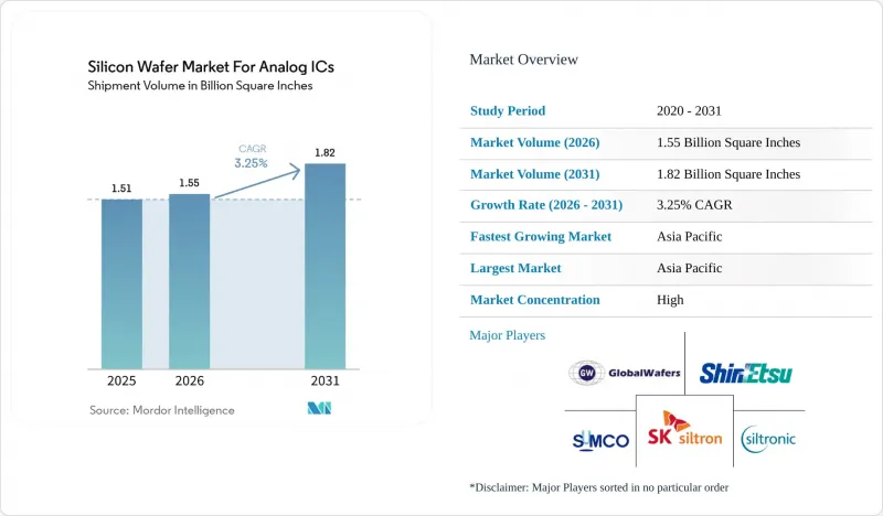
Mordor Intelligence에 의하면, 아날로그 IC용 실리콘 웨이퍼 시장 출하량 기반 시장 규모는 2025년에 15억 1,000만 평방인치로 평가되었습니다. 2026년에는 15억 5,000만 평방인치, 2031년까지 18억 2,000만 평방인치에 이르고, 2026-2031년에 걸쳐 CAGR 3.25%를 나타낼 것으로 예측됩니다.
본 보고서는 웨이퍼 직경(150mm 이하, 200mm, 300mm), 웨이퍼 유형(프라임 폴리시, 에피택셜, SOI, 특수 실리콘), 최종 사용자(가전, 산업용, 자동차용, 기타), 지역(북미, 유럽, 아시아태평양, 남미, 중동 및 아프리카)에 따라 분류되어 있습니다. 시장 전망은 출하량(제곱인치) 기준으로 제시되어 있습니다.
아날로그 IC용 실리콘 웨이퍼 시장 동향 및 전망
저전력 아날로그 IC용 300mm 파운드리 생산 능력 확대
각 파운드리 업체들은 28nm를 초과하는 아날로그 노드를 대상으로 한 300mm 생산 라인에 수십억 달러 규모의 투자를 진행하고 있습니다. 이는 수율이 최첨단 로직에 미치지 못하는 경우에도 더 큰 웨이퍼를 사용함으로써 다이 비용을 절감할 수 있기 때문입니다. GlobalWafers의 75억 달러 규모 텍사스 프로젝트와 Siltronic의 20억 유로 규모 독일·싱가포르 계획은 이러한 전환의 규모를 여실히 보여주고 있습니다. 텍사스 기기는 리처드슨과 리하이에서 이 모델을 재현하고 있으며, CHIPS 보조금을 활용하여 자본 집약도를 상쇄하고 있습니다. SEMI의 예측에 따르면, 2026년부터 2028년에 걸쳐 아날로그, 파워, 디스크리트용 팹이 410억 달러 이상의 장비 투자를 흡수할 것으로 전망됩니다. 이러한 투자를 통해 아날로그 IC용 실리콘 웨이퍼 시장은 2020년대 말까지 300mm 생산으로 중심이 이동하게 될 것입니다.
EV 급속 충전 분야의 고전압 PMIC 수요 증가
800V를 초과하는 전압에서 작동하는 급속 충전 시스템에서는 치명적인 파손을 방지하기 위해 결함 밀도가 0.05 cm-² 이하인 에피택셜 실리콘 웨이퍼가 필요합니다. 르네사스, 아날로그 디바이스, NXP는 모두 ISO 26262 안전 기준을 충족하는 정격 42V-60V의 PMIC를 출시하고 있습니다. 국제에너지기구(IEA)는 2025년 전기차 판매 대수가 1,700만 대를 넘어섰으며, 이에 따라 350kW 충전기와 관련된 기판 수요가 확대될 것으로 예측됩니다. 따라서, 저항률을 엄격하게 관리할 수 있는 특수 실리콘 공급업체들은 자동차용 IDM 업체들과 장기 공급 계약을 체결하고 있습니다.
아날로그 IDM의 주기적인 설비 투자
자동차 및 산업용 고객들의 주문을 신속하게 조정하기 위해, 아날로그 IDM은 팹 가동률을 낮출 수밖에 없습니다. 신에츠 케미칼은 2025년 10월 자동차 재고 조정 이후 200mm 웨이퍼 수요가 위축되었다고 보고했습니다. 텍사스 기기는 2024년 제출한 서류에서 제조 장비 도입 연기를 발표했습니다. 이러한 주기적인 지연은 웨이퍼의 평균 판매 가격(ASP)에 하락 압력을 가하고, 공급업체의 운전 자본과 관련된 위험을 크게 높이고 있습니다.
부문별 분석
2025년, 200mm급은 아날로그 IC용 실리콘 웨이퍼 시장 점유율의 74.74%를 차지했습니다. 그러나 텍사스 기기(Texas Instruments)와 전 세계 웨이퍼 제조업체들이 더 큰 기판에서 저전력 아날로그 공정 인증을 추진하고 있는 만큼, 300mm 부문은 2031년까지 연평균 성장률(CAGR) 3.89%를 기록하며 성장할 것으로 전망됩니다. 팹 전환 시 공통 리소그래피 실적를 활용함으로써, 아날로그 IDM은 노드 미세화를 진행하지 않아도 다이 비용을 30-40% 절감할 수 있습니다. 조기 도입 기업들은 레이아웃 설계 규정이 유연하고 허용 범위가 넓은 PMIC 및 데이터 컨버터 제품군에 주력함으로써, 300mm 설비 투자에 대한 신속한 회수를 확실히 하고 있습니다.
고전압 사이리스터 및 연구개발(R&D) 파일럿 용도를 위한 최대 150mm 규모의 틈새 시장은 여전히 존재하지만, 장비 제조업체들이 툴셋을 200mm 리퍼비시 라인으로 확대함에 따라 이 시장은 계속해서 축소될 것으로 보입니다. 한편, 200mm의 생산 능력은 여전히 부족합니다. 자동차 부문의 재고 변동으로 인해 단기적인 수요 둔화가 나타나고 있지만, 산업용 로봇 및 재생에너지 부문 수요가 성숙 노드공급을 계속해서 흡수하고 있습니다. 예측 기간 동안 300mm 공급 증가로 인해 직경별 구성 비율이 재조정되면서, 아날로그 IC용 실리콘 웨이퍼 시장은 더욱 다각화된 비용 구조로 전환될 것으로 보입니다.
지역별 분석
아시아태평양은 2025년 출하량의 67.77%를 차지하며, 아날로그 IC용 실리콘 웨이퍼 시장에서 가장 큰 점유율을 확보했을 뿐만 아니라, 2031년 연평균 성장률(CAGR)도 4.06%로 1위를 유지할 전망입니다. 대만 반도체 제조 회사(TSMC), 싱구이(Simgui), SK 실트론의 생산 능력 확충은 고전압 PMIC 및 mm파 RF 칩을 지원하는 300mm 생산 라인에 집중되어 있습니다. 중국의 국내 조달 노력 덕분에 세계 경기 순환이 둔화되더라도 수요는 견조한 추세를 보이고 있으며, 한편 일본의 Rapidus 프로젝트는 혼합 신호 노드 시장으로의 병행 진출을 뒷받침하고 있습니다. 한국은 성숙한 노드의 신뢰성이 요구되는 자동차용 전자기기 수출 기업들과 가까운 위치에 있다는 이점이 있습니다. 해당 지역에 팹과 소재 공급업체가 밀집해 있는 것은 물류 주기를 단축하고, 비용 면에서의 우위를 강화하고 있습니다.
북미는 2025년에 15%대 중반의 점유율을 차지했으며, CHIPS법에 따른 인센티브가 신규 아날로그 생산 능력의 위험을 완화하고 있어 세계 평균을 웃도는 속도로 성장하고 있습니다. GlobalWafers, Texas Instruments, 온세미는 300mm 공장 건설 또는 확장을 추진 중이며, 2020년대 후반까지 총 월 100만 장 이상의 웨이퍼 생산을 목표로 하고 있습니다. 자동차, 방위, 데이터센터 분야의 고객들은 지정학적 리스크를 헤지하고 인증 절차를 단축하기 위해 국내 조달을 선호하고 있습니다. 이러한 동향은 기존 200mm 생산 라인의 가동률을 높이는 동시에, 신규 그린필드 부지에 대한 자금 조달을 뒷받침하고 있습니다.
유럽은 인피니언(Infineon), ST마이크로일렉트로닉스(STMicroelectronics) 등 세계 파운드리 업체들의 확장을 지원하는 EU 칩 법의 보조금에 힘입어 두 자릿수 초반 시장 점유율을 유지했습니다. 독일 드레스덴 거점은 자동차용 혼합 신호 소자 생산의 중심지로 부상하고 있는 반면, 이탈리아 카타니아 공장은 실리콘 카바이드 에피택시에 주력하고 있습니다. 영국과 프랑스는 RF-SOI나 센서 등급 웨이퍼와 같은 특수 제품의 생산에 기여하고 있지만, 주요 연마 완료 웨이퍼의 대량 공급에 대해서는 수입에 의존하고 있습니다. 남미, 중동 및 아프리카의 합계 점유율은 여전히 5% 미만이지만, 재생에너지 및 통신 프로젝트에 따른 틈새 수요가 점차 생겨나고 있어, 향후 10년 후반에는 현지에서 연마 및 슬라이싱 사업이 유치될 가능성이 있습니다.
기타 혜택
- 엑셀 형식 시장 예측(ME) 시트
- 3개월간의 애널리스트 지원
자주 묻는 질문
목차
제1장 서론
제2장 조사 방법
제3장 주요 요약
제4장 시장 구도
제5장 시장 규모 및 성장 예측(지역별 출하량)
제6장 경쟁 구도
제7장 시장 기회 및 향후 전망
KTHAccording to Mordor Intelligence, the silicon wafer market for analog ICs industry size in terms of shipment volume is projected to be 1.51 Billion Square Inches in 2025, 1.55 Billion Square Inches in 2026, and reach 1.82 Billion Square Inches by 2031, growing at a CAGR of 3.25% from 2026 to 2031.

This report is Segmented by Wafer Diameter (Up To 150 Mm, 200 Mm, 300 Mm), Wafer Type (Prime Polished, Epitaxial, Silicon-On-Insulator, Specialty Silicon), End-User (Consumer Electronics, Industrial, Automotive, and More), and Geography (North America, Europe, Asia-Pacific, South America, Middle East, Africa). The Market Forecasts are Provided in Terms of Shipment Volume (Square Inches).
Insights and Trends of Silicon Wafer Market For Analog ICs
Capacity Expansion by 300 mm Foundries for Power-Efficient Analog ICs
Foundries are channeling multi-billion-dollar outlays into 300 mm lines targeting analog nodes above 28 nm, because larger wafers trim die costs even when yields lag those of leading-edge logic. GlobalWafers' USD 7.5 billion Texas project and Siltronic's EUR 2 billion German-Singapore plan illustrate the scale of this pivot. Texas Instruments is replicating the model in Richardson and Lehi, using CHIPS grants to offset the capital intensity. SEMI forecasts that analog, power, and discrete fabs will absorb more than USD 41 billion in equipment from 2026-2028. These investments position the silicon wafer market for analog ICs to shift its center of gravity toward 300 mm production by the end of the decade.
Growing Demand for High-Voltage PMICs in EV Fast-Charging
Fast-charging systems operating above 800 V require epitaxial silicon wafers with defect densities below 0.05 cm-2 to prevent catastrophic breakdown. Renesas, Analog Devices, and NXP have all introduced PMICs rated 42 V-60 V that meet ISO 26262 safety levels. The International Energy Agency expects EV sales to exceed 17 million units in 2025, amplifying substrate demand tied to 350 kW chargers. Specialty silicon suppliers that can guarantee tight control of resistivity are therefore securing long-term supply contracts with automotive IDMs.
Cyclical Capital Expenditure of Analog IDMs
Automotive and industrial customers adjust orders quickly, forcing analog IDMs to throttle fab utilization. Shin-Etsu Chemical reported softer 200 mm volumes after automotive inventory corrections in October 2025. In its 2024 filings, Texas Instruments announced the postponement of its tool installations. These cyclical delays exert downward pressure on wafer Average Selling Prices (ASPs) and significantly increase the risks associated with working capital for suppliers.
Other drivers and restraints analyzed in the detailed report include:
- Analog Front-End Integration in 5G Massive-MIMO Radios
- Transition to Wide-Bandgap Gate Drivers Requiring Ultra-Low Defect Wafers
- Supply Tightness of High-Purity Polysilicon Feedstock
For complete list of drivers and restraints, kindly check the Table Of Contents.
Segment Analysis
The 200 mm class captured 74.74% of the analog ICs silicon wafer market share in 2025. However, the 300 mm category is on track for a 3.89% CAGR to 2031 as Texas Instruments and GlobalWafers qualify power-efficient analog flows on larger substrates. Fab conversions exploit common lithography footprints, allowing analog IDMs to slice 30%-40% from die cost without node shrinks. Early adopters focus on PMICs and data-converter families whose layouts tolerate relaxed design rules, ensuring quick returns on 300 mm capex.
A residual niche of up to 150 mm persists for high-voltage thyristors and R&D pilots, but will continue to contract as equipment makers extend their toolsets to 200 mm refurb lines. Meanwhile, 200 mm capacity remains constrained; inventory swings in automotive cause short-term softness, yet industrial robot and renewable-energy demand continue to absorb mature-node supply. Over the forecast, rising 300 mm availability will rebalance the diameter mix, nudging the silicon wafer market for analog ICs toward a more diversified cost base.
Geography Analysis
Asia-Pacific commanded 67.77% of 2025 shipments, giving the region the largest share of the analog ICs silicon wafer market and a leading 4.06% CAGR through 2031. Capacity additions by Taiwan Semiconductor Manufacturing Company, Simgui, and SK Siltron are concentrated on 300 mm lines that support high-voltage PMICs and millimeter-wave RF chips. China's drive for domestic sourcing keeps demand resilient even when global cycles soften, while Japan's Rapidus project anchors a parallel push into mixed-signal nodes. Korea benefits from proximity to automotive electronics exporters that require mature-node reliability. The region's tight cluster of fabs and materials vendors shortens logistics cycles and reinforces its cost advantage.
North America held a mid-teens share in 2025 and is growing faster than the global average as CHIPS Act incentives de-risk new analog capacity. GlobalWafers, Texas Instruments, and Onsemi are building or expanding 300 mm plants that collectively aim to reach more than 1 million wafers per month by the late 2020s. Automotive, defense, and datacenter customers prefer domestic sourcing to hedge geopolitical risk and shorten qualification loops. These trends improve utilization of existing 200 mm lines while underpinning financing for new greenfield sites.
Europe maintained a low-double-digit share, helped by EU Chips Act subsidies supporting Infineon, STMicroelectronics, and GlobalFoundries' expansions. Germany's Dresden hub is emerging as a center for automotive-grade mixed-signal production, while Italy's Catania facility focuses on silicon-carbide epitaxy. The United Kingdom and France contribute specialty output for RF-SOI and sensor-grade wafers, yet rely on imports for prime polished volume. South America, the Middle East, and Africa together remain below a 5% share, though renewable-energy and telecom projects are creating niche demand that may invite local polishing or slicing operations later in the decade.
- Shin-Etsu Chemical Co., Ltd.
- SUMCO Corporation
- GlobalWafers Co., Ltd.
- Siltronic AG
- SK Siltron Co., Ltd.
- Wafer Works Corporation
- Soitec S.A.
- Siltronix Silicon Technologies
- MEMC Electronic Materials Inc.
- Shanghai Simgui Technology Co., Ltd.
- Topsil Semiconductor Materials A/S
- Okmetic Oyj
- Addison Engineering, Inc.
- Grinm Semiconductor Materials Co., Ltd.
- GT Advanced Technologies Inc.
- Wafer World Inc.
- Coherent Corp. (II-VI)
- Nova Electronic Materials
- Elkem ASA
- Mitsui Mining & Smelting Co., Ltd.
Additional Benefits:
- The market estimate (ME) sheet in Excel format
- 3 months of analyst support
TABLE OF CONTENTS
1 INTRODUCTION
- 1.1 Study Assumptions and Market Definition
- 1.2 Scope of the Study
2 RESEARCH METHODOLOGY
3 EXECUTIVE SUMMARY
4 MARKET LANDSCAPE
- 4.1 Market Overview
- 4.2 Market Drivers
- 4.2.1 Capacity Expansion by 300 mm Foundries for Power-Efficient Analog ICs
- 4.2.2 Growing Demand for High-Voltage PMICs in EV Fast-Charging
- 4.2.3 Analog Front-End Integration in 5G Massive-MIMO Radios
- 4.2.4 Transition to Wide-Bandgap Gate Drivers Requiring Ultra-Low Defect Wafers
- 4.2.5 On-shoring Incentives under CHIPS and EU Chips Acts
- 4.2.6 Adoption of AI-Based Process Control Reducing Scrap Rates
- 4.3 Market Restraints
- 4.3.1 Cyclical Capital Expenditure of Analog IDMs
- 4.3.2 Supply Tightness of High-Purity Polysilicon Feedstock
- 4.3.3 Yield Challenges in >=200 mm SOI Wafers for mmWave RF
- 4.3.4 Sustainability Pressures on Water and Energy Usage
- 4.4 Industry Value-Chain Analysis
- 4.5 Regulatory Landscape
- 4.6 Technology Analysis
- 4.7 Impact of Macroeconomic Factors
- 4.8 Porter's Five Forces Analysis
- 4.8.1 Bargaining Power of Suppliers
- 4.8.2 Bargaining Power of Buyers
- 4.8.3 Threat of New Entrants
- 4.8.4 Threat of Substitutes
- 4.8.5 Intensity of Competitive Rivalry
5 MARKET SIZE AND GROWTH FORECASTS (SHIPMENT IN AREA)
- 5.1 By Wafer Diameter
- 5.1.1 Up to 150 mm
- 5.1.2 200 mm
- 5.1.3 300 mm
- 5.2 By Wafer Type
- 5.2.1 Prime Polished
- 5.2.2 Epitaxial
- 5.2.3 Silicon-on-Insulator (SOI)
- 5.2.4 Specialty Silicon (High-Resistivity, Power, Sensor-Grade)
- 5.3 By End-user
- 5.3.1 Consumer Electronics
- 5.3.1.1 Mobile and Smartphones
- 5.3.1.2 PCs and Servers
- 5.3.2 Industrial
- 5.3.3 Telecommunications
- 5.3.4 Automotive
- 5.3.5 Other End-user Applications
- 5.3.1 Consumer Electronics
- 5.4 By Geography
- 5.4.1 North America
- 5.4.1.1 United States
- 5.4.1.2 Canada
- 5.4.1.3 Mexico
- 5.4.2 Europe
- 5.4.2.1 Germany
- 5.4.2.2 United Kingdom
- 5.4.2.3 France
- 5.4.2.4 Rest of Europe
- 5.4.3 Asia-Pacific
- 5.4.3.1 China
- 5.4.3.2 Japan
- 5.4.3.3 India
- 5.4.3.4 South Korea
- 5.4.3.5 Taiwan
- 5.4.3.6 Rest of Asia-Pacific
- 5.4.4 South America
- 5.4.5 Middle East
- 5.4.6 Africa
- 5.4.1 North America
6 COMPETITIVE LANDSCAPE
- 6.1 Market Concentration
- 6.2 Strategic Moves
- 6.3 Market Share Analysis
- 6.4 Company Profiles (includes Global Level Overview, Market Level Overview, Core Segments, Financials as available, Strategic Information, Market Rank/Share, Products and Services, Recent Developments)
- 6.4.1 Shin-Etsu Chemical Co., Ltd.
- 6.4.2 SUMCO Corporation
- 6.4.3 GlobalWafers Co., Ltd.
- 6.4.4 Siltronic AG
- 6.4.5 SK Siltron Co., Ltd.
- 6.4.6 Wafer Works Corporation
- 6.4.7 Soitec S.A.
- 6.4.8 Siltronix Silicon Technologies
- 6.4.9 MEMC Electronic Materials Inc.
- 6.4.10 Shanghai Simgui Technology Co., Ltd.
- 6.4.11 Topsil Semiconductor Materials A/S
- 6.4.12 Okmetic Oyj
- 6.4.13 Addison Engineering, Inc.
- 6.4.14 Grinm Semiconductor Materials Co., Ltd.
- 6.4.15 GT Advanced Technologies Inc.
- 6.4.16 Wafer World Inc.
- 6.4.17 Coherent Corp. (II-VI)
- 6.4.18 Nova Electronic Materials
- 6.4.19 Elkem ASA
- 6.4.20 Mitsui Mining & Smelting Co., Ltd.
7 MARKET OPPORTUNITIES AND FUTURE OUTLOOK
- 7.1 White-Space and Unmet-Need Assessment
