
|
시장보고서
상품코드
2065514
고속 인쇄회로기판 시장 : 시장 점유율 분석, 업계 동향 및 통계, 성장 예측(2026-2031년)High-Speed PCB - Market Share Analysis, Industry Trends & Statistics, Growth Forecasts (2026 - 2031) |
||||||
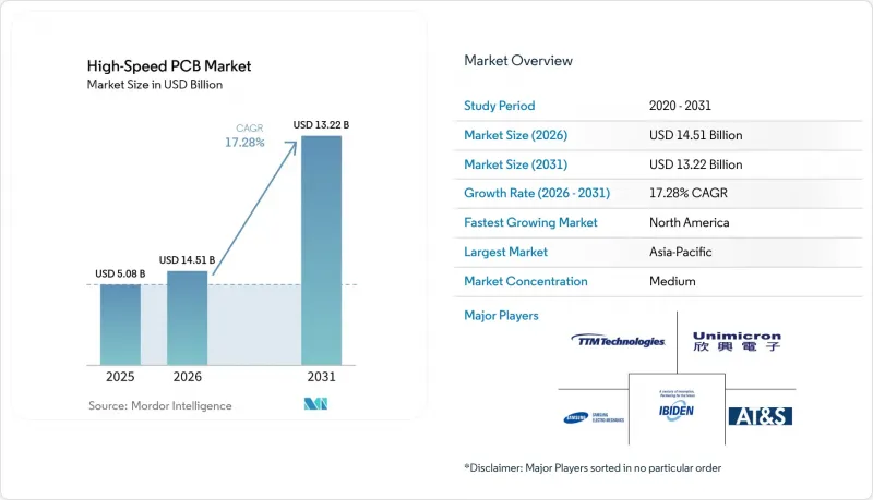
고속 인쇄회로기판 시장 규모는 2025년 50억 8,000만 달러로 평가되었고, 2026년에는 59억 6,000만 달러로 추정되고, 게다가 2031년까지 132억 2,000만 달러로 확대될 전망이며, 2026-2031년 CAGR 17.28%를 나타낼 것으로 예측되고 있습니다.

본 보고서는 PCB 유형별(12층 이상의 다층 고속 인쇄회로기판, HDI PCB 등), 데이터 전송 속도별(최대 25Gbps, 25-56Gbps, 56-112 Gbps, 112 Gbps 이상), 재료 유형별(표준 FR-4, 중간 손실 재료 등), 최종 이용 산업별(하이퍼스케일 데이터센터, AI/ML 클러스터, 클라우드 서비스 제공업체 등), 지역별로 분류되어 있습니다. 시장 전망은 금액(달러) 기준으로 제시되어 있습니다.
세계의 고속 인쇄회로기판 시장 동향 및 인사이트
AI 및 ML GPU 클러스터에 대한 수요 증가
2025년에 도입될 생성형 AI 랙은 70개 이상의 GPU를 통합하여 총 상호 연결 대역폭을 1테라비트/초 이상으로 높이고, 112 Gbps의 신호 무결성을 유지하면서 PCB의 전류 한계를 1,800암페어 이상으로 끌어올립니다. 각 하이퍼스케일러 기업들은 범용 서버 보드에 비해 3-4배 높은 비용 프리미엄을 감당하고 있습니다. 이는 지연 시간이 1마이크로초 증가할 때마다 대규모 언어 모델(LLM)의 쿼리를 통한 수익에 직접적인 영향을 미치기 때문입니다. 자본 예산을 통해 장기 공급 계약이 뒷받침되고 있기 때문에 VIA-IN-PAD HDI 기술을 습득한 제조업체는 수년에 걸친 대량 발주 확약을 확보하고 있습니다. 또한, 설계가 복잡해짐에 따라 비반복 설계 비용(NRE)도 증가하여, 이로 인해 평균 판매 가격이 상승하고, 고속 인쇄회로기판 시장의 이익 규모가 확대되고 있습니다.
56-112 Gbps SerDes 및 PCIe 6.0의 급속한 보급
2025년에 도입될 PCIe 6.0에서는 레인당 대역폭이 2배로 늘어나지만, 전압 마진이 축소됨에 따라 PCIe 4.0에서는 사소한 문제였던 트레이스 손실이 이제는 미션 크리티컬한 문제가 되고 있습니다. CPU 제조업체가 설정한 36데시벨의 신호대잡음비(SNR) 임계값을 유지하기 위해서는 유전 정접이 0.002 미만인 초저손실 에폭시 또는 PTFE 라미네이트를 사용한 서버 기판이 현재 요구되고 있습니다. 이 기준을 충족할 수 있는 라미네이트 공급업체는 전 세계적으로 단 4곳에 불과하며, 공급이 집중되면서 리드타임이 길어지고 가격도 급등하고 있습니다. 설계 회사는 스텁 길이와 백드릴링을 최적화하기 위해 3차원 전자기장 시뮬레이션에 대한 의존도를 높이고 있으며, 프로젝트당 엔지니어링 툴에 대한 지출이 증가하고 있습니다.
초고속 데이터 전송 속도에서의 열 관리 과제
112 Gbps로 작동하는 SerDes 채널은 레인당 5와트 이상의 열을 방출하기 때문에 16레인 디바이스의 경우 10 cm² 미만의 영역에 80와트가 집중되어 기판 온도를 유리전이 온도의 한계치 근처까지 상승시킵니다. 인텔의 추산에 따르면, 기판 수준의 냉각 솔루션은 현재 모듈 비용의 최대 22%를 차지하고 있습니다. 액침 냉각은 유전율을 변화시키고 임피던스를 최대 12옴까지 변화시키기 때문에 트레이스 형상을 보정해야 하므로 설계가 더욱 복잡해집니다. 그 결과, AI 서버의 현장 반품률이 기존 시스템보다 40% 높아지면서 보증 충당금이 급증하고 있습니다.
부문별 분석
2025년에는 12층 이상의 다층 기판이 매출의 38%를 차지했으며, 듀얼 소켓 서버의 주력 플랫폼으로서의 역할을 더욱 확고히 하고 있습니다. 이 기판들은 56Gbps 워크로드에서 밀도, 비용, 제조 용이성 간의 균형이 잘 잡혀 있어, 고속 인쇄회로기판 시장의 가장 큰 비중을 차지하고 있습니다. 그러나 칩렛 아키텍처가 가속기 로드맵 전반에 걸쳐 확산됨에 따라, 기판형 PCB 시장은 연평균 성장률(CAGR) 18.28%를 기록하며 성장하고 있습니다. AMD, 인텔, 엔비디아가 모듈당 150-200달러 상당의 유기 인터포저를 양산에 도입함에 따라, 이러한 기판형 포맷을 위한 고속 인쇄회로기판 시장은 확대될 것으로 보입니다.
기판형 PCB에는 10마이크론 미만의 라인 및 스페이스와 10,000비아/mm²를 초과하는 비아 밀도가 요구되며, 이는 첨단 패키징과 기존 PCB 영역의 중간에 위치합니다. AT&S나 이비덴과 같은 제조업체들은 이러한 수요에 대응하기 위해 각각 5억 달러 이상을 투자하여 말레이시아와 일본에 새로운 생산 라인을 구축하고 있습니다. HDI 기판은 공간이 제한된 엣지 서버에서 여전히 중요한 위치를 차지하고 있지만, 백플레인은 마이크로비아 밀도보다 낮은 크로스 토크를 중시하는 스토리지 패브릭 분야에서 계속해서 주류를 이루고 있습니다. 이러한 혼합 기술 스택은 단일 틈새 시장에 특화된 기업보다 다각적인 공급업체에 유리하게 작용합니다.
PCIe 5.0 및 100G 이더넷의 도입을 원동력으로, 56-112 Gbps 링크용으로 설계된 기판은 2025년 매출의 41%를 차지했습니다. 그럼에도 불구하고, 112 Gbps 이상의 부문은 연평균 성장률(CAGR) 18.18%로 확대될 것으로 예측되며, 고속 인쇄회로기판 시장 전체의 성장에 가장 빠르게 기여할 것으로 보입니다. 이 부문에서 고속 인쇄회로기판 시장 규모가 확대된 것은 30인치 배선에서 30데시벨 미만의 삽입 손실이 요구되는 PCIe 6.0 마더보드와 800G 스위치의 라인 카드에 기인합니다.
이러한 요건을 충족하기 위해서는 설계자가 비아 스텁을 5밀 미만으로 단축하고, ±3%의 제어 임피던스 배선 공차를 적용하며, PTFE 또는 탄화수소계 라미네이트로 전환해야 합니다. 67 기가헤르츠 벡터 네트워크 분석기 1대의 가격이 현재 30만 달러에 달하기 때문에 설비 투자 수요가 증가하고 있지만, 이러한 계측 기기가 없으면 제조업체는 하이퍼스케일 인증을 획득할 수 없습니다. 엣지 컴퓨팅이나 소규모 사무실 네트워크에서는 여전히 최대 25Gbps까지의 저속 기판이 주류를 이루고 있지만, AI 추론이 보급됨에 따라 수익은 점차 고속 데이터 전송 속도 영역으로 이동하고 있습니다.
지역별 분석
아시아태평양은 대만, 중국, 일본, 한국의 견실한 생산 능력을 바탕으로 2025년 매출의 68%를 차지했습니다. 이 국가들은 드릴 가공, 도금, 조립 공정에 이르는 광범위한 생산 능력을 보유하고 있으며, 이러한 시설들은 고도로 통합된 캠퍼스 내에 집중되어 있습니다. 이 지역공급업체들은 규모의 경제와 라미네이트 및 구리박 생산 시설과의 전략적 근접성 덕분에 큰 혜택을 누리고 있습니다. 이러한 근접성 덕분에, 특히 주류 AI 서버 용도에서 고속 인쇄회로기판 시장은 비용 경쟁력을 유지하고 있습니다. 또한, 연구개발 센터가 동일한 거점에 집적되어 있어 공정의 혁신과 반복이 신속하게 진행되며, 경쟁이 치열한 세계 시장에서 해당 지역 내 제품 출시까지 소요되는 시간을 단축한다는 중요한 우위를 확보하고 있습니다.
북미는 생산량은 적지만, 2031년까지 연평균 성장률(CAGR)이 18.38%로 가장 빠른 성장이 전망되고 있는 지역이며, 국가 안보 관련 워크로드에 대해 국내 조립을 의무화하는 ‘주권 컴퓨팅’ 요건이 성장의 원동력이 되고 있습니다. 'CHIPS and Science Act' 등의 프로그램을 통해 PCB 및 반도체 시설에 대한 보조금이 지원되고 있는 만큼, TTM Technologies와 같은 제조업체들은 뉴욕의 초고밀도 회로 기판(HDI) 사업 확장에 1억 5,000만 달러를 배정하고 있습니다. 이러한 리쇼어링은 공급망 리스크를 부분적으로 상쇄하고, 미국 내 방위 기관 및 클라우드 사업자를 대상으로 한 리드타임을 단축함으로써, 해당 지역의 고속 인쇄회로기판 시장 점유율을 확대되고 있습니다.
유럽에서는 다품종·고복잡성에 대한 집중이 계속되고 있습니다. 오스트리아에 거점을 둔 AT&S와 독일의 각 거점은 고가형 기판 및 유리 코어 기판에 투자하고 있지만, 아시아와 비교하면 절대적인 생산량은 여전히 적은 임베디드니다. 남미, 중동 및 아프리카는 여전히 틈새 시장에 머물러 있으며, AI 서버용이 아닌 통신용 및 산업용 기판을 공급하고 있습니다. 전반적으로 지역별 양극화가 심화되고 있으며, 생산량은 아시아에 편중되는 반면, 부가가치와 회복탄력성은 북미 및 일부 유럽 공장에 집중되어 있습니다.
기타 혜택 :
- 엑셀 형식 시장 예측(ME) 시트
- 3개월간의 애널리스트 지원
자주 묻는 질문
목차
제1장 서론
제2장 조사 방법
제3장 주요 요약
제4장 시장 구도
제5장 시장 규모 및 성장 예측
제6장 경쟁 구도
제7장 시장 기회 및 향후 전망
AJYAccording to Mordor Intelligence, the high-speed PCB market size is expected to increase from USD 5.08 billion in 2025 to USD 5.96 billion in 2026 and to USD 13.22 billion by 2031, growing at a CAGR of 17.28% over 2026-2031.
This report is Segmented by PCB Type (Multilayer High-Speed PCBs 12+ Layers, HDI PCBs, and More), Data Rate Capability (Up To 25 Gbps, 25-56 Gbps, 56-112 Gbps, and 112 Gbps+), Material Type (Standard FR-4, Mid-Loss Materials, and More), End-Use Industry (Hyperscale Data Centers AI/ML Clusters, Cloud Service Providers, and More), and Geography. The Market Forecasts are Provided in Terms of Value (USD).
Global High-Speed PCB Market Trends and Insights
Growing Demand for AI and ML GPU Clusters
Generative AI racks introduced in 2025 integrate more than 70 GPUs and drive aggregate interconnect bandwidth above 1 terabit per second, pushing PCB current limits past 1,800 amperes while retaining 112 Gbps signal integrity. Hyperscalers absorb the three-to-four-fold cost premium over general-purpose server boards because every microsecond of latency directly affects revenue from large-language-model queries. Capital budgets support long-term supply agreements, so fabricators that master via-in-pad HDI techniques secure multi-year volume commitments. The design complexity also increases non-recurring engineering fees, which raise average selling prices and expand the high-speed PCB market profit pool.
Rapid Adoption of 56-112 Gbps SerDes and PCIe 6.0
The PCIe 6.0 rollout in 2025 doubles per-lane bandwidth but shrinks voltage margins, making trace losses that were minor at PCIe 4.0 now mission-critical. Server boards built on ultra-low-loss epoxy or PTFE laminates with dissipation factors below 0.002 are now required to sustain a 36 decibel signal-to-noise threshold set by CPU vendors. Only four laminate suppliers worldwide can meet this standard, so supply concentration extends lead times and hardens pricing. Design houses increasingly rely on 3-D electromagnetic simulation to optimize stub length and back-drilling, elevating engineering tool spend per project.
Thermal Management Challenges at Ultra-High Data Rates
SerDes channels operating at 112 Gbps dissipate more than 5 watts per lane, so a 16-lane device concentrates 80 watts over less than 10 cm2, driving board temperatures close to the glass-transition limit. Intel estimates that board-level cooling solutions now consume up to 22% of module costs. Immersion cooling alters dielectric constants, shifting impedance by up to 12 ohms, which forces trace-geometry compensation and raises design complexity. Resulting field-return rates for AI servers run 40% higher than traditional systems, inflating warranty reserves.
Other drivers and restraints analyzed in the detailed report include:
- Increasing Layer Counts and HDI Adoption
- Expansion of Hyperscale Data Center Capacity
- Supply Chain Disruptions and Material Lead Times
For complete list of drivers and restraints, kindly check the Table Of Contents.
Segment Analysis
Multilayer boards with 12 or more layers accounted for 38% of revenue in 2025, underscoring their role as the workhorse platform for dual-socket servers. These boards account for the largest slice of the high-speed PCB market share because they balance density, cost, and manufacturability for 56 Gbps workloads. Substrate-like PCBs, however, are climbing at an 18.28% CAGR as chiplet architectures propagate across accelerator roadmaps. The high-speed PCB market for these substrate-like formats will grow as AMD, Intel, and NVIDIA bring organic interposers priced at USD 150-200 per module into production.
Substrate-like boards demand line-and-space below 10 microns and via densities over 10,000 vias/mm2, positioning them halfway between advanced packaging and traditional PCB realms. Fabricators such as AT&S and Ibiden channel more than USD 500 million each into new Malaysian and Japanese lines to address this demand. HDI boards retain relevance in edge servers where space is scarce, while backplanes continue to dominate storage fabrics that prize low-crosstalk over micro-via density. This mixed technology stack favors diversified suppliers rather than single-niche shops.
Boards engineered for 56-112 Gbps links secured 41% of 2025 revenue, powered by PCIe 5.0 and 100G Ethernet deployments. Even so, the 112 Gbps-plus cohort is projected to rise at an 18.18% CAGR, making it the fastest contributor to overall high-speed PCB market growth. High-speed printed circuit board market size gains in this category reflect PCIe 6.0 motherboards and 800G switch line cards that require insertion losses below 30 decibels across 30-inch traces.
Meeting these budgets obliges designers to shorten via stubs below 5 mils, adopt controlled-impedance routing tolerances of +-3%, and shift to PTFE or hydrocarbon-based laminates. Capital needs escalate because a single 67 gigahertz vector network analyzer now costs USD 300,000, yet without such metrology, fabricators cannot win hyperscale qualifications. Lower-speed boards up to 25 Gbps remain prevalent in edge compute and small-office networking, but revenue gradually gravitates toward the higher data-rate tiers as AI inference proliferates.
Geography Analysis
Asia-Pacific accounted for 68% of 2025 sales, driven by the robust manufacturing capabilities of Taiwan, China, Japan, and South Korea. These countries host extensive capacities across drilling, plating, and assembly processes, consolidated within highly integrated campuses. The region's vendors benefit significantly from economies of scale and their strategic proximity to laminate and copper-foil production facilities. This proximity ensures the high-speed PCB market remains cost-competitive, particularly for mainstream AI server applications. Additionally, the presence of co-located research and development centers fosters rapid process innovation and iteration, providing the region with a critical time-to-market advantage in a highly competitive global market.
North America, though smaller in volume, is the fastest-growing region, with a 18.38% CAGR through 2031, driven by sovereign-compute mandates requiring domestic assembly for national-security workloads. Programs such as the CHIPS and Science Act steer subsidies toward PCB and semiconductor facilities, so fabricators like TTM Technologies earmark USD 150 million for ultra-HDI expansion in New York. This reshoring partially offsets supply-chain risk and shortens lead times for U.S. defense and cloud operators, enlarging the regional high-speed PCB market share.
Europe keeps a high-mix, high-complexity focus. Austria-based AT&S and Germany-based sites invest in substrate-like and glass-core boards that command premium pricing, though absolute volumes remain modest compared with Asia. South America, the Middle East, and Africa remain niche, supplying telecom and industrial boards rather than AI servers. Overall, a bifurcated geography emerges, with volume tilting toward Asia while value and resilience tilt toward North America and select European plants.
- TTM Technologies Inc.
- Unimicron Technology Corp.
- Ibiden Co., Ltd.
- Samsung Electro-Mechanics Co., Ltd.
- AT&S Austria Technologie and Systemtechnik AG
- Compeq Manufacturing Co., Ltd.
- Nan Ya Printed Circuit Board Corp.
- Shennan Circuits Co., Ltd.
- Zhen Ding Technology Holding Limited
- Tripod Technology Corp.
- CMK Corporation
- Meiko Electronics Co., Ltd.
- WUS Printed Circuit Co., Ltd.
- Chin-Poon Industrial Co., Ltd.
- Sanmina Corporation
- Flex Ltd. (Multek)
- Kyocera Corporation
- RayMing Technology
- Advanced Circuits Inc.
- Shenzhen Kinwong Electronic Co., Ltd.
Additional Benefits:
- The market estimate (ME) sheet in Excel format
- 3 months of analyst support
TABLE OF CONTENTS
1 INTRODUCTION
- 1.1 Study Assumptions and Market Definition
- 1.2 Scope of the Study
2 RESEARCH METHODOLOGY
3 EXECUTIVE SUMMARY
4 MARKET LANDSCAPE
- 4.1 Market Overview
- 4.2 Market Drivers
- 4.2.1 Growing Demand for AI and ML GPU Clusters in Data Centers
- 4.2.2 Rapid Adoption of 56-112 Gbps SerDes and PCIe 6.0 Standards
- 4.2.3 Increasing Layer Counts and HDI Adoption in Server Boards
- 4.2.4 Expansion of Hyperscale Data Center Capacity Worldwide
- 4.2.5 Transition to Chiplet Architectures Requiring High-Speed Interposers
- 4.2.6 Emergence of Glass Core Substrates and SLB Technology
- 4.3 Market Restraints
- 4.3.1 Thermal Management Challenges at Ultra-High Data Rates
- 4.3.2 Supply Chain Disruptions and Material Lead Times
- 4.3.3 Yield Losses in Ultra-Low-Loss Laminate Fabrication
- 4.3.4 Regulatory Scrutiny on Export of Advanced Packaging Equipment
- 4.4 Impact of Macroeconomic Factors on the Market
- 4.5 Industry Value Chain Analysis
- 4.6 Regulatory Landscape
- 4.7 Technological Outlook
- 4.8 Porter's Five Forces Analysis
- 4.8.1 Bargaining Power of Suppliers
- 4.8.2 Bargaining Power of Buyers
- 4.8.3 Threat of New Entrants
- 4.8.4 Threat of Substitutes
- 4.8.5 Intensity iof Competitive Rivalry
5 MARKET SIZE AND GROWTH FORECASTS (VALUE)
- 5.1 By Sensor Type
- 5.1.1 Multilayer High-Speed PCBs (12+ Layers)
- 5.1.2 HDI PCBs
- 5.1.3 Ultra-Low-Loss / High-Frequency PCBs
- 5.1.4 Backplane PCBs
- 5.1.5 Substrate-Like PCBs
- 5.2 By Data Rate Capability
- 5.2.1 Up to 25 Gbps
- 5.2.2 25-56 Gbps
- 5.2.3 56-112 Gbps
- 5.2.4 112 Gbps+
- 5.3 By Material Type
- 5.3.1 Standard FR-4
- 5.3.2 Mid-Loss Materials
- 5.3.3 Low-Loss Materials
- 5.3.4 Ultra-Low-Loss Materials
- 5.4 By End-User Industry
- 5.4.1 Hyperscale Data Centers (AI/ML Clusters)
- 5.4.2 Cloud Service Providers
- 5.4.3 Enterprise HPC
- 5.4.4 Government / Research Labs
- 5.5 By Geography
- 5.5.1 North America
- 5.5.1.1 United States
- 5.5.1.2 Canada
- 5.5.1.3 Mexico
- 5.5.2 South America
- 5.5.2.1 Brazil
- 5.5.2.2 Argentina
- 5.5.2.3 Rest of South America
- 5.5.3 Europe
- 5.5.3.1 United Kingdom
- 5.5.3.2 Germany
- 5.5.3.3 France
- 5.5.3.4 Italy
- 5.5.3.5 Rest of Europe
- 5.5.4 Asia-Pacific
- 5.5.4.1 China
- 5.5.4.2 Japan
- 5.5.4.3 India
- 5.5.4.4 South Korea
- 5.5.4.5 Rest of Asia-Pacific
- 5.5.5 Middle East and Africa
- 5.5.5.1 Middle East
- 5.5.5.1.1 United Arab Emirates
- 5.5.5.1.2 Saudi Arabia
- 5.5.5.1.3 Rest of Middle East
- 5.5.5.2 Africa
- 5.5.5.2.1 South Africa
- 5.5.5.2.2 Egypt
- 5.5.5.2.3 Rest of Africa
- 5.5.5.1 Middle East
- 5.5.1 North America
6 COMPETITIVE LANDSCAPE
- 6.1 Market Concentration
- 6.2 Strategic Moves
- 6.3 Market Share Analysis
- 6.4 Company Profiles (includes Global Level Overview, Market Level Overview, Core Segments, Financials as available, Strategic Information, Market Rank/Share, Products and Services, Recent Developments)
- 6.4.1 TTM Technologies Inc.
- 6.4.2 Unimicron Technology Corp.
- 6.4.3 Ibiden Co., Ltd.
- 6.4.4 Samsung Electro-Mechanics Co., Ltd.
- 6.4.5 AT&S Austria Technologie and Systemtechnik AG
- 6.4.6 Compeq Manufacturing Co., Ltd.
- 6.4.7 Nan Ya Printed Circuit Board Corp.
- 6.4.8 Shennan Circuits Co., Ltd.
- 6.4.9 Zhen Ding Technology Holding Limited
- 6.4.10 Tripod Technology Corp.
- 6.4.11 CMK Corporation
- 6.4.12 Meiko Electronics Co., Ltd.
- 6.4.13 WUS Printed Circuit Co., Ltd.
- 6.4.14 Chin-Poon Industrial Co., Ltd.
- 6.4.15 Sanmina Corporation
- 6.4.16 Flex Ltd. (Multek)
- 6.4.17 Kyocera Corporation
- 6.4.18 RayMing Technology
- 6.4.19 Advanced Circuits Inc.
- 6.4.20 Shenzhen Kinwong Electronic Co., Ltd.
7 MARKET OPPORTUNITIES AND FUTURE OUTLOOK
- 7.1 White-Space and Unmet-Need Assessment
