

|
시장보고서
상품코드
2098477
칩렛 기반 GPU 시장 : 시장 점유율 분석, 업계 동향 및 통계, 성장 예측(2026-2031년)Chiplet-Based GPU - Market Share Analysis, Industry Trends & Statistics, Growth Forecasts (2026 - 2031) |
||||||
 Mordor Intelligence
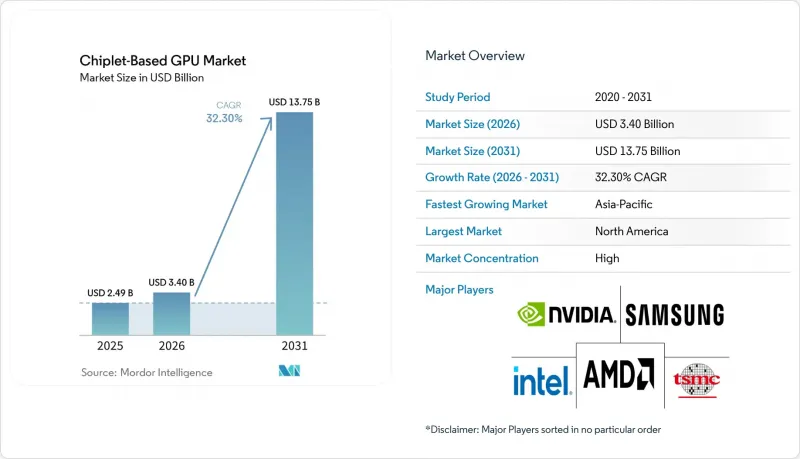
Mordor Intelligence에 의하면, 칩렛 기반 GPU 시장 규모는 2025년에 24억 9,000만 달러로 평가되었고, 2026년 34억 달러에서 2031년까지 137억 5,000만 달러에 이를 것으로 예측되며, 2026-2031년 CAGR 32.30%로 성장할 전망입니다.
본 보고서는 프로세서 유형별(디스크리트/고성능 컴퓨팅용 GPU 치플릿 등), 패키징 기술별(2.5D 인터포저 및 브리지 기반 패키징 등), 상호 연결 규격별(UCIe 기반 다이 간 상호 연결 등), 최종 사용자 산업별(데이터센터 및 클라우드 컴퓨팅, 고성능 컴퓨팅 등), 그리고 지역별로 분류되어 있습니다. 시장 전망은 금액(달러) 기준으로 제시되어 있습니다.
세계의 칩렛 기반 GPU 시장 동향 및 인사이트
AI 및 HPC에서 레티클 크기 한계의 극복
주요 AI 훈련 시스템이 더 이상 모놀리식 스케일링에만 의존할 수 없게 됨에 따라, 레티클 크기 한계는 칩렛 기반 GPU 시장에서 직접적인 설계상의 제약 요인이 되고 있습니다. NVIDIA는 2개의 레티클 크기의 연산용 치플릿과 8개의 HBM4 스택을 결합한 'Vera Rubin'을 통해 이 과제를 양산 단계로 전환하고, 2026년 하반기에 양산 출하를 시작할 예정입니다. 또한 인텔 파운드리 측은 EMIB 2.5D 상호 연결이 2026년에는 레티클 크기의 8배 이상, 2028년까지는 12배 이상을 지원하도록 설계되었다고 밝혔으며, 이는 최첨단 GPU 프로그램에서 다이 수준의 스케일링을 대신해 패키지 수준의 스케일링이 주류로 자리 잡고 있음을 보여줍니다. 이러한 변화는 성능, 수율 관리, 소프트웨어 호환성을 저해하지 않으면서 여러 다이에 걸쳐 연산, 메모리, I/O를 분할할 수 있는 기업에게 유리하게 작용합니다. AMD는 2026년 하반기부터 시작되는 Helios 도입을 MI450X 칩렛 GPU와 연계함으로써 이러한 방향성을 더욱 강조했습니다. 이는 레티클 에스케이프가 더 이상 실험적인 아키텍처의 경로가 아니라, 생산 플랫폼 계획의 일부가 되었음을 뒷받침합니다.
HBM을 중심으로 한 2.5D 및 3D 패키징 채택
HBM 통합은 경쟁력 있는 AI 가속기에 있어 필수 요건이 되었으며, 2.5D 및 3D 패키징은 칩렛 기반 GPU 시장에서 가장 강력한 성장 동력 중 하나가 되었습니다. TSMC에 따르면, 해당사의 CoWoS 생산 능력은 2023년 말 월 15,000 웨이퍼에서 2025년 말에는 월 70,000-80,000 웨이퍼로 확대되며, 2026년 말까지 월 120, 000-130,000 웨이퍼를 목표로 하고 있습니다. 이러한 생산 능력 확대에도 불구하고, 주요 GPU 프로그램은 여전히 인터포저 및 HBM 통합 능력의 조기 배정에 의존하고 있어, 제품 출시 시기나 고객 납품 측면에서 패키징 접근성은 전략적으로 중요한 요소로 남아 있습니다. 삼성 역시 고밀도 멀티다이 구조를 향한 로드맵의 일환으로, 첨단 이종 통합 및 하이브리드 구리 본딩을 강조하고 있으며, 이는 GPU와 메모리의 보다 긴밀한 결합을 향한 움직임을 뒷받침하고 있습니다. 그 결과, 칩렛 기반 GPU 시장에서는 로직 노드에 대한 접근과 마찬가지로 패키징 준비 상태가 제품의 경쟁력을 좌우하는 요인이 되고 있습니다.
고밀도 GPU 패키지의 열 및 전력 공급 병목 현상
열 및 전력 공급 제한은 칩렛 기반 GPU 시장에서 여전히 가장 해결하기 어려운 실행상의 과제이며, 특히 AI 패키지의 전력 소비량이 기존의 공랭식으로는 효율적으로 유지할 수 없는 수준을 넘어 증가하고 있는 상황에서는 더욱 그렇습니다. 『Semiconductor Engineering』지의 보고에 따르면, 4개 이상의 HBM 스택을 통합한 AI 가속기 패키지는 현재 디바이스당 1kW를 넘어서는 추세이며, 이로 인해 패키지 스택 전체에 걸쳐 냉각, 전력 정합성 및 장기적인 신뢰성에 대한 요구가 높아지고 있습니다. 이 잡지는 또한, 뒷면에서 전력을 공급하는 방식은 표면에서 전력을 공급하는 방식에 비해 국부적인 핫스팟 온도를 상승시킬 가능성이 있어, 고밀도 AI 패키지 설계에 있어 추가적인 상충 요소가 발생한다고 지적하고 있습니다. 이러한 제약 사항이 채택을 방해하는 것은 아니지만, 양산 개시 지연, 통합 비용 증가, 그리고 첨단 열 공동 설계를 성공적으로 수행할 수 있는 팀의 수 감소로 이어질 가능성이 있습니다. 따라서 칩렛 기반 GPU 시장의 성능 향상은 초기 단계부터 냉각 아키텍처, 전력 계획, 패키지 레이아웃이 유기적으로 연계되어 작동하는 데 점점 더 의존하게 되고 있습니다.
부문 분석
멀티다이 SoC 및 적응형 구성의 GPU 칩렛이 프로세서 유형 수요를 주도하여, 2025년에는 칩렛 기반 GPU 시장 점유율의 53.81%를 차지한 것으로 평가되었습니다. AI 가속기용 GPU 칩렛 및 이종 GPU 모듈은 2031년까지 연평균 성장률(CAGR) 33.28%를 나타낼 것으로 예측되며, 칩렛 기반 GPU 시장에서 가장 빠르게 확대될 프로세서 유형이 될 전망입니다. 이러한 성장 가속화는 더 큰 모놀리식 다이가 아닌, 리트리크 에스케이프, 더 높은 메모리 대역폭 및 모듈식 확장이 필요한 훈련 시스템으로의 전환에 기인합니다. NVIDIA의 Vera Rubin 플랫폼은 듀얼 컴퓨트 칩렛 아키텍처와 8개의 HBM4 스택을 채택하고 있으며, 2026년 하반기 양산 출하를 목표로 하는 상용 제품 주기를 통해 이러한 변화를 여실히 보여주고 있습니다.
멀티다이 SoC 구성은 최첨단 AI 가속기와 같은 전체 비용 프로파일을 감당할 필요 없이 모듈형 연산을 필요로 하는 엔터프라이즈, 자동차, 소비자용 용도에 적합하기 때문에 가장 폭넓은 기반을 유지하고 있습니다. 재사용 가능한 치플릿을 통해 벤더는 검증된 I/O 및 메모리 구조를 계승하면서 새로운 노드를 위해 연산 다이만 업데이트할 수 있으므로, 프로세서 구성도 변화하고 있습니다. 이는 설계 주기가 긴 프로젝트에서 중요하며, 이러한 프로젝트에서는 절대적인 피크 처리량과 마찬가지로 인증 프로세스 및 플랫폼의 연속성이 중시됩니다. Helios 시스템 내의 MI450X를 둘러싼 AMD의 2026년 인프라 계획은 칩렛 기반 GPU 시장에서 프로세서 선택이 현재 랙 수준의 도입 모델과 직접적으로 연결되어 있음을 보여줍니다.
2025년, 2.5D 인터포저 및 브리지 기반 패키징은 칩렛 기반 GPU 시장의 47.48%를 차지하며 주요 패키징 기법으로서 선두 자리를 유지했습니다. 이 부문이 우위를 유지한 이유는 높은 대역폭 메모리와 고밀도 다이 간 배선이 필요한 주요 AI GPU 프로그램에서 CoWoS가 여전히 실용적인 생산 경로이기 때문입니다. TSMC가 발표한 로드맵에 따르면, 2026년 CoWoS의 생산 능력이 급증할 것으로 나타나, 이 플랫폼이 첨단 GPU 상용화에서 얼마나 중심적인 역할을 하고 있는지를 뒷받침하고 있습니다. 또한 AMD는 2026년 5월, PTI와의 공동 개발을 통해 2.5D 패널 기반의 Elevated Fanout Bridge(EBF) 상호 연결을 인증함으로써 공급 측면의 선택지를 더욱 확대했습니다. 생산이 안정적으로 진행된다면, 이를 통해 기존의 웨이퍼 기반 공정에 따르는 부담이 경감될 가능성이 있습니다.
3D 적층 및 하이브리드 본딩을 통한 패키징은 2031년까지 연평균 성장률(CAGR) 33.19%를 나타낼 것으로 예측되며, 칩렛 기반 GPU 시장에서 가장 빠르게 성장하는 패키징 분야가 될 전망입니다. 3D 집적의 매력은 상호 연결 경로의 단축, 메모리 결합의 밀집화, 그리고 패키지 실적를 확대하지 않고도 대역폭을 증가시킬 수 있다는 점에 있습니다. Samsung Electronics는 자사의 첨단 이종 집적 로드맵에 고밀도 멀티다이 구조를 위한 하이브리드 구리 본딩이 포함되어 있으며, 이것이 패키지 스케일링의 다음 단계를 뒷받침할 것이라고 밝혔습니다. 예측 기간 동안 2.5D가 수량 면에서 주도적인 위치를 유지하는 한편, 대역폭 밀도나 시스템 효율성 측면에서 더 높은 집적의 복잡성이 정당화되는 프로그램에서는 3D 패키징이 점유율을 확대해 나갈 것으로 전망됩니다.
지역별 분석
2025년, 북미는 칩렛 기반 GPU 시장 점유율의 46.94%를 차지하며 최대 지역 시장이 되었습니다. 이 지역은 미국 전역에 NVIDIA, AMD, 인텔, 하이퍼스케일러, EDA 벤더, 그리고 첨단 패키징 파트너가 집중되어 있다는 이점이 있습니다. 2025년 9월 NVIDIA가 인텔과 맞춤형 데이터센터 및 PC 제품에 관한 제휴를 체결한 것은 코어 아키텍처 결정 및 생태계 제휴가 여전히 북미에서 이루어지고 있음을 보여줍니다. 또한 인텔은 고성능 AI 시스템을 목표로 한 EMIB 및 Foveros 로드맵을 통해 패키징 및 파운드리 기술 분야에서도 이 지역의 강점을 유지하고 있습니다.
2025년에도 아시아태평양은 2위의 규모를 유지하며, 칩렛 기반 GPU 시장의 주요 생산 거점으로 자리매김했습니다. 이 지역에는 TSMC의 CoWoS 및 SoIC 생산 능력, 삼성의 첨단 이종 통합 프로그램, 주요 HBM 공급망, 그리고 대규모 OSAT 사업이 집중되어 있습니다. TSMC의 CoWoS 로드맵과 삼성의 첨단 패키징 로드맵은 아시아태평양이 왜 첨단 GPU 조립 제조 분야에서 계속해서 주도권을 유지하고 있는지를 보여줍니다. AMD는 2026년 5월, 패키징, 브리지 상호 연결 개발 및 Helios 생산과 관련하여 대만의 생태계에 100억 달러 이상을 투자하겠다고 발표하며 이러한 의존 관계를 더욱 공고히 했습니다. 이로 인해 칩렛 기반 GPU 시장에서 아시아태평양은 단기적인 실행 위험과 단기적인 기회의 중심에 위치하게 될 것입니다.
중동 및 아프리카은 2031년까지 연평균 성장률(CAGR) 32.98%로 확대될 것으로 예상되며, 칩렛 기반 그래픽 처리 장치(GPU) 시장에서 가장 빠르게 성장하는 지역 부문이 될 전망입니다. 이 지역의 성장은 국가 주도의 AI 프로그램, 데이터센터 확충, 그리고 첨단 컴퓨팅 인프라에 대한 현지 접근성을 확보하기 위한 광범위한 노력과 밀접하게 연관되어 있습니다. 유럽은 슈퍼컴퓨팅 수요, 자동차용 컴퓨팅 프로그램, 그리고 패키징 선택에 영향을 미치는 재료 규정 요건을 통해 계속해서 중요한 시장으로 남아 있습니다. 남미에서는 도입이 아직 초기 단계에 있으며, 수요는 치플릿 GPU 하드웨어의 직접 조달보다는 클라우드 기반 AI 컴퓨팅에 대한 접근에 중점을 두고 있습니다. 이러한 지역별 추세를 종합해 보면, 북미의 설계 주도력, 아시아태평양의 탄탄한 제조거점, 그리고 중동 및 아프리카에서 빠르게 형성되고 있는 새로운 수요가 시장을 견인하고 있음을 알 수 있습니다.
기타 혜택 :
- 엑셀 형식 시장 예측(ME) 시트
- 3개월간의 애널리스트 지원
자주 묻는 질문
목차
제1장 서론
제2장 조사 방법
제3장 주요 요약
제4장 시장 구도
제5장 시장 규모 및 성장 예측
제6장 경쟁 구도
제7장 시장 기회 및 향후 전망
AJY 26.08.07According to Mordor Intelligence, the chiplet-based GPU market size is projected to be USD 2.49 billion in 2025, USD 3.4 billion in 2026, and reach USD 13.75 billion by 2031, growing at a CAGR of 32.30% from 2026 to 2031.
This report is Segmented by Processor Type (Discrete / High-Performance Compute GPU Chiplets, and More), Packaging Technology (2. 5D Interposer and Bridge-Based Packaging, and More), Interconnect Standard (UCIe-Based Die-To-Die Interconnect, and More), End-User Industry (Data Centers and Cloud Computing, High-Performance Computing, and More), and Geography. The Market Forecasts are Provided in Terms of Value (USD).
Global Chiplet-Based GPU Market Trends and Insights
AI and HPC Reticle-Limit Escape
The reticle-size limit has become a direct design constraint in the chiplet-based GPU market, as leading AI training systems can no longer rely solely on monolithic scaling. NVIDIA moved this issue into commercial production with Vera Rubin, which combines 2 reticle-sized compute chiplets with 8 HBM4 stacks, and is scheduled for volume shipment in the second half of 2026. Intel Foundry also stated that the EMIB 2.5D interconnect is engineered to support more than 8 times the reticle size in 2026 and 12 times by 2028, indicating that package-level scaling is replacing die-level scaling in advanced GPU programs. This change favors companies that can partition compute, memory, and I/O across several dies without losing performance, yield discipline, or software alignment. AMD reinforced that direction when it linked Helios deployments beginning in the second half of 2026 to MI450X chiplet GPUs, which confirms that reticle escape is now part of production platform planning rather than an experimental architecture path.
HBM-Centered 2.5D and 3D Package Adoption
HBM integration has become a baseline requirement for competitive AI accelerators, making 2.5D and 3D packaging among the strongest growth engines in the chiplet-based GPU market. TSMC said its CoWoS capacity expanded from 15,000 wafers per month at the end of 2023 to 70,000-80,000 wafers per month at the end of 2025, and it is targeting 120,000-130,000 wafers per month by the end of 2026. Even with that ramp, major GPU programs still depend on early allocation of interposer and HBM integration capacity, which keeps packaging access strategically important for launch timing and customer fulfillment. Samsung also highlighted advanced heterogeneous integration and hybrid copper bonding as part of its roadmap for dense multi-die structures, which supports the move toward tighter GPU and memory coupling. The result is a chiplet-based GPU market where packaging readiness now shapes product competitiveness almost as much as logic-node access.
Thermal and Power-Delivery Bottlenecks In Dense GPU Packages
Thermal and power-delivery limits remain the hardest execution problem in the chiplet-based GPU market, especially as AI package power rises beyond levels that conventional air cooling can sustain efficiently. Semiconductor Engineering reported that AI accelerator packages integrating 4 or more HBM stacks are now pushing past 1 kW per device, which raises cooling, power integrity, and long-run reliability demands across the full package stack. The same publication also noted that backside power delivery can increase local hotspot temperatures relative to frontside approaches, adding another layer of trade-offs in dense AI package design. These limits do not prevent adoption, but they can delay ramps, increase integration costs, and reduce the number of teams that can execute advanced thermal co-design successfully. That is why performance gains in the chiplet-based GPU market are becoming more dependent on cooling architecture, power planning, and package layout working together from the start.
Other drivers and restraints analyzed in the detailed report include:
- Advanced-Node NRE Reduction Through IP Reuse
- 5G, Cloud, and Networking Demand For Disaggregated Silicon
- Immature Cross-Vendor Interoperability and IP Liability
For complete list of drivers and restraints, kindly check the Table Of Contents.
Segment Analysis
GPU chiplets in multi-die SoCs and adaptive configurations drove processor-type demand, with 53.81% of the chiplet-based GPU market share in 2025. AI accelerator GPU chiplets and heterogeneous GPU modules are projected to grow at a 33.28% CAGR through 2031, making them the fastest-expanding processor type in the chiplet-based GPU market. That acceleration follows the move toward training systems that require reticle escape, higher memory bandwidth, and modular scaling rather than a larger monolithic die. NVIDIA's Vera Rubin platform illustrates this shift with a dual-compute chiplet architecture and 8 HBM4 stacks, in a commercial product cycle aimed at second-half 2026 volume shipments.
Multi-die SoC configurations kept the broadest base because they fit enterprise, automotive, and consumer programs that need modular compute without the full cost profile of frontier AI accelerators. The processor mix is also shifting because reusable chiplets let vendors carry forward validated I/O and memory structures while updating only the compute die for a new node. That matters in programs with longer design cycles, where qualification discipline and platform continuity are as important as absolute peak throughput. AMD's 2026 infrastructure planning around MI450X inside the Helios system shows how processor choices are now being tied directly to rack-level deployment models in the chiplet-based GPU market
2.5D interposer and bridge-based packaging accounted for 47.48% of the chiplet-based GPU market in 2025, maintaining its lead as the leading packaging approach. This segment stayed ahead because CoWoS remains the practical production path for leading AI GPU programs that need high-bandwidth memory and dense die-to-die routing. TSMC's published roadmap shows a sharp ramp in CoWoS capacity through 2026, confirming how central this platform has become to advanced GPU commercialization. AMD also added another supply-side option in May 2026 by qualifying a 2.5D panel-based Elevated Fanout Bridge interconnect with PTI, which could ease pressure on conventional wafer-based flows if production execution remains stable.
3D-stacked and hybrid-bonded packaging is projected to grow at a 33.19% CAGR through 2031, making it the fastest-growing packaging segment in the chiplet-based GPU market. The appeal of 3D integration stems from shorter interconnect paths, tighter memory coupling, and the ability to increase bandwidth without expanding the package footprint. Samsung stated that its advanced heterogeneous integration roadmap includes hybrid copper bonding for dense multi-die structures, which supports the next stage of package scaling. Over the forecast period, 2.5D should remain the volume leader while 3D packaging gains share in programs where bandwidth density and system efficiency justify higher integration complexity.
Complete Report Scope:
- By Processor Type
- Discrete / High-Performance Compute GPU Chiplets
- Integrated / Consumer GPU Chiplets
- AI Accelerator GPU Chiplets / Heterogeneous GPU Modules
- GPU Chiplets in Multi-Die SoC / Adaptive Configurations
- Other Chiplet-Based GPU Variants
- By Packaging Technology
- 2.5D Interposer and Bridge-Based Packaging
- 3D Stacked and Hybrid-Bonded Packaging
- Fan-Out and RDL-Based Advanced Packaging
- Organic Substrate-Based Multi-Die Packaging
- Other Packaging Technologies
- By Interconnect Standard
- UCIe-Based Die-to-Die Interconnect
- Proprietary Die-to-Die Interconnect
- Hybrid Open-Standard and Proprietary Architectures
- By End-user Industry
- Data Centers and Cloud Computing
- High-Performance Computing
- Consumer Computing
- Automotive and Mobility
- Telecommunications and Networking
- Industrial and Edge AI
- Aerospace and Defense
- Other End-user Industries
- By Geography
- North America
- United States
- Canada
- Mexico
- Europe
- Germany
- United Kingdom
- France
- Italy
- Rest of Europe
- Asia-Pacific
- China
- Japan
- South Korea
- India
- Southeast Asia
- Rest of Asia-Pacific
- South America
- Middle East and Africa
- North America
Geography Analysis
North America accounted for 46.94% of the chiplet-based GPU market share in 2025, making it the largest regional market. The region benefits from the concentration of NVIDIA, AMD, Intel, hyperscalers, EDA vendors, and advanced packaging partners across the United States. NVIDIA's September 2025 collaboration with Intel on custom data center and PC products shows how core architecture decisions and ecosystem alliances are still set in North America. Intel also keeps the region strong in packaging and foundry technology through EMIB and Foveros roadmaps aimed at high-performance AI systems.
Asia-Pacific remained the second-largest region and the main production base for the chiplet-based GPU market in 2025. The region concentrates CoWoS and SoIC capacity at TSMC, advanced heterogeneous integration programs at Samsung, major HBM supply chains, and large OSAT operations. TSMC's CoWoS roadmap and Samsung's advanced packaging roadmap show why Asia-Pacific continues to control the manufacturing side of advanced GPU assembly. AMD reinforced that dependence in May 2026, when it announced more than USD 10 billion in investments in the Taiwan ecosystem, tied to packaging, bridge interconnect development, and Helios production. This leaves Asia-Pacific at the center of near-term execution risk and near-term opportunity for the chiplet-based GPU market.
The Middle East and Africa are projected to expand at a 32.98% CAGR through 2031, making it the fastest-growing regional segment in the chiplet-based graphics processing unit (GPU) market. Growth in this region is tied to sovereign AI programs, data center build-outs, and broader efforts to secure local access to advanced compute infrastructure. Europe remains important through supercomputing demand, automotive computing programs, and materials compliance requirements that affect packaging choices. South America is still earlier in adoption, with demand centered more on access to cloud-based AI compute than on direct procurement of chiplet GPU hardware. Together, these regional patterns show a market led by North American design control, Asia-Pacific manufacturing depth, and faster new demand formation in the Middle East and Africa.
- Advanced Micro Devices, Inc.
- Intel Corporation
- NVIDIA Corporation
- Taiwan Semiconductor Manufacturing Company Limited
- Samsung Electronics Co., Ltd.
- Broadcom Inc.
- Marvell Technology, Inc.
- International Business Machines Corporation
- MediaTek Inc.
- Achronix Semiconductor Corporation
- ASE Technology Holding Co., Ltd.
- Amkor Technology, Inc.
- Synopsys, Inc.
- Cadence Design Systems, Inc.
- Alphawave IP Group plc
- Ayar Labs, Inc.
- Renesas Electronics Corporation
- Tenstorrent Holdings, Inc.
- Apple Inc.
- Arm Holdings plc
Additional Benefits:
- The market estimate (ME) sheet in Excel format
- 3 months of analyst support
TABLE OF CONTENTS
1 INTRODUCTION
- 1.1 Study Assumptions and Market Definition
- 1.2 Scope of the Study
2 RESEARCH METHODOLOGY
3 EXECUTIVE SUMMARY
4 MARKET LANDSCAPE
- 4.1 Market Overview
- 4.2 Market Drivers
- 4.2.1 AI and HPC Reticle-Limit Escape
- 4.2.2 HBM-Centered 2.5D and 3D Package Adoption
- 4.2.3 Advanced-Node NRE Reduction Through IP Reuse
- 4.2.4 5G, Cloud, and Networking Demand for Disaggregated Silicon
- 4.2.5 Optical I/O Chiplets for Rack-Scale AI Scale-Up
- 4.2.6 KGD Testing and UCIe Alliances De-Risk Merchant Chiplets
- 4.3 Market Restraints
- 4.3.1 Thermal and Power-Delivery Bottlenecks in Dense GPU Packages
- 4.3.2 Immature Cross-Vendor Interoperability and IP Liability
- 4.3.3 Yield Compounding and Test-Cost Inflation in KGD Flows
- 4.3.4 CoWoS, Interposer, Substrate, and Optical-Packaging Bottlenecks
- 4.4 Impact of Macroeconomic Factors on the Market
- 4.5 Industry Value Chain Analysis
- 4.6 Regulatory Landscape
- 4.7 Technological Outlook
- 4.8 Porter's Five Forces Analysis
- 4.8.1 Bargaining Power of Suppliers
- 4.8.2 Bargaining Power of Buyers
- 4.8.3 Threat of New Entrants
- 4.8.4 Threat of Substitutes
- 4.8.5 Competitive Rivalry
5 MARKET SIZE AND GROWTH FORECASTS (VALUE)
- 5.1 By Processor Type
- 5.1.1 Discrete / High-Performance Compute GPU Chiplets
- 5.1.2 Integrated / Consumer GPU Chiplets
- 5.1.3 AI Accelerator GPU Chiplets / Heterogeneous GPU Modules
- 5.1.4 GPU Chiplets in Multi-Die SoC / Adaptive Configurations
- 5.1.5 Other Chiplet-Based GPU Variants
- 5.2 By Packaging Technology
- 5.2.1 2.5D Interposer and Bridge-Based Packaging
- 5.2.2 3D Stacked and Hybrid-Bonded Packaging
- 5.2.3 Fan-Out and RDL-Based Advanced Packaging
- 5.2.4 Organic Substrate-Based Multi-Die Packaging
- 5.2.5 Other Packaging Technologies
- 5.3 By Interconnect Standard
- 5.3.1 UCIe-Based Die-to-Die Interconnect
- 5.3.2 Proprietary Die-to-Die Interconnect
- 5.3.3 Hybrid Open-Standard and Proprietary Architectures
- 5.4 By End-user Industry
- 5.4.1 Data Centers and Cloud Computing
- 5.4.2 High-Performance Computing
- 5.4.3 Consumer Computing
- 5.4.4 Automotive and Mobility
- 5.4.5 Telecommunications and Networking
- 5.4.6 Industrial and Edge AI
- 5.4.7 Aerospace and Defense
- 5.4.8 Other End-user Industries
- 5.5 By Geography
- 5.5.1 North America
- 5.5.1.1 United States
- 5.5.1.2 Canada
- 5.5.1.3 Mexico
- 5.5.2 Europe
- 5.5.2.1 Germany
- 5.5.2.2 United Kingdom
- 5.5.2.3 France
- 5.5.2.4 Italy
- 5.5.2.5 Rest of Europe
- 5.5.3 Asia-Pacific
- 5.5.3.1 China
- 5.5.3.2 Japan
- 5.5.3.3 South Korea
- 5.5.3.4 India
- 5.5.3.5 Southeast Asia
- 5.5.3.6 Rest of Asia-Pacific
- 5.5.4 South America
- 5.5.5 Middle East and Africa
- 5.5.1 North America
6 COMPETITIVE LANDSCAPE
- 6.1 Market Concentration
- 6.2 Strategic Moves
- 6.3 Market Positioning Analysis
- 6.4 Company Profiles (includes Global Level Overview, Market Level Overview, Core Segments, Financials as available, Strategic Information, Market Rank/Share, Products and Services, Recent Developments)
- 6.4.1 Advanced Micro Devices, Inc.
- 6.4.2 Intel Corporation
- 6.4.3 NVIDIA Corporation
- 6.4.4 Taiwan Semiconductor Manufacturing Company Limited
- 6.4.5 Samsung Electronics Co., Ltd.
- 6.4.6 Broadcom Inc.
- 6.4.7 Marvell Technology, Inc.
- 6.4.8 International Business Machines Corporation
- 6.4.9 MediaTek Inc.
- 6.4.10 Achronix Semiconductor Corporation
- 6.4.11 ASE Technology Holding Co., Ltd.
- 6.4.12 Amkor Technology, Inc.
- 6.4.13 Synopsys, Inc.
- 6.4.14 Cadence Design Systems, Inc.
- 6.4.15 Alphawave IP Group plc
- 6.4.16 Ayar Labs, Inc.
- 6.4.17 Renesas Electronics Corporation
- 6.4.18 Tenstorrent Holdings, Inc.
- 6.4.19 Apple Inc.
- 6.4.20 Arm Holdings plc
7 MARKET OPPORTUNITIES AND FUTURE OUTLOOK
- 7.1 White-Space and Unmet-Need Assessment


