

|
시장보고서
상품코드
2098491
옵티컬 GPU 인터커넥트 시장 : 점유율 분석, 업계 동향 및 통계, 성장 예측(2026-2031년)Opitcal GPU Interconnect - Market Share Analysis, Industry Trends & Statistics, Growth Forecasts (2026 - 2031) |
||||||
 Mordor Intelligence
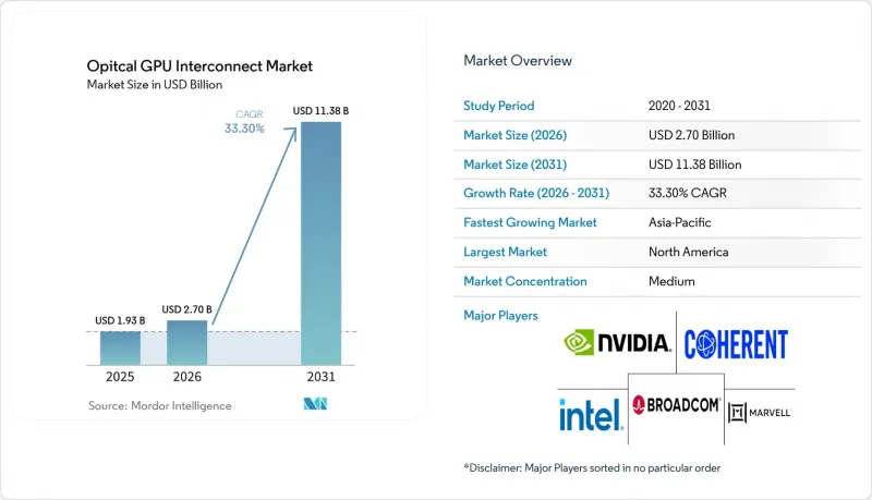
Mordor Intelligence에 의하면, 옵티컬 GPU 인터커넥트 시장 규모는 2025년 19억 3,000만 달러, 2026년 27억 달러에서 2031년까지 113억 8,000만 달러로 확대한다고 예측되고 있어 2026년부터 2031년까지 연평균 복합 성장률(CAGR)은 33.30%를 나타낼 전망입니다.
본 보고서는 제품 유형(광트랜시버, 액티브 광케이블 등), 인터커넥트 수준(칩 간, 기판 간, 랙 수준 등), 광섬유 모드(단일 모드 광섬유, 다중 모드 광섬유), 데이터 전송 속도(40 Gbps 미만, 40-100 Gbps 등), 용도(데이터 통신 등), 지역별로 분류되어 있습니다. 시장 전망은 금액(달러) 기준으로 제시되어 있습니다.
세계 옵티컬 GPU 인터커넥트 시장 동향 및 인사이트
AI 훈련 및 추론에서의 대역폭 수요 증가
2025년에 이르러 AI 훈련 클러스터는 수천 대에서 수만 대의 GPU로 확대될 것이며, 추론 부하가 높은 모델이 보편화됨에 따라 추론 시스템도 같은 방향으로 나아가고 있습니다. 이는 현대의 GPU 시스템 내에서 계산 자체뿐만 아니라 데이터 전송이 에너지의 대부분을 소비하게 되었기 때문에 중요한 의미를 지닙니다. 이러한 변화로 인해 인터커넥트 대역폭이 클러스터 설계의 실질적인 제한 요인이 되었으며, 이것이 옵티컬 GPU 인터커넥트 시장 전체 수요를 직접 뒷받침하고 있습니다. 광 I/O를 둘러싼 업계 논의에서도, 추론 워크로드에서 과거에는 주로 훈련 환경과 연관되었던 저지연 패브릭이 점점 더 필요해지고 있음을 알 수 있습니다. 그 결과, 옵티컬 GPU 인터커넥트 시장에 대한 향후 투자가 더 이상 최첨단 모델의 훈련에만 국한되지 않게 되면서, 광 링크에 대한 수요 기반은 더욱 확대되고 있습니다.
GPU 클러스터에서 구리 인터커넥트의 전력 및 도달 거리 한계
구리 링크는 속도와 거리가 증가함에 따라 신호 손실이 커지는 문제를 안고 있으며, 이러한 물리적 한계가 현재 대규모 GPU 클러스터의 시스템 레이아웃에 영향을 미치고 있습니다. NVIDIA의 설명에 따르면, NVL72 랙에서 NVLink 속도의 구리 링크 전송 거리는 매우 짧게 제한되어 있었기 때문에 스위치의 배치는 섀시 내에서 엄격하게 제약될 수밖에 없었습니다. 시스템이 1개 랙에서 8개 랙으로 확장됨에 따라, 옵티컬 GPU 인터커넥트 시장에서 광통신은 단순한 유용한 선택지에서 필수 요건으로 변화하고 있습니다. 『npj Nanophotonics』 저널의 조사에 따르면, 구리 기반 확장 네트워크에서는 광 링크에 비해 훨씬 적은 수의 XPU로도 코히런트 도메인이 상한선에 도달하는 것으로 밝혀졌으며, 이로 인해 설계자들이 향후 클러스터 규모를 고려하는 방식도 변화하고 있습니다. 전력 소비 역시 이러한 전환의 또 다른 이유입니다. 구리를 많이 사용하는 인터커넥트은 랙의 전력을 소모하지만, 옵티컬 GPU 인터커넥트 시장에서 운영자들은 그 전력을 오히려 연산 처리를 위해 확보하고자 하기 때문입니다.
고급 포토닉 패키징 및 테스트의 높은 비용
옵티컬 GPU 인터커넥트 시장에서 코패키징형 광 모듈의 비용 구조는 표준 플러그인식 모듈보다 훨씬 더 높습니다. 패키징에는 CMOS 전자 회로, 실리콘 포토닉스, III-V족 소재가 결합되어 있어 조립이 더 어려워지므로, 단위당 비용이 높은 수준을 유지하고 있습니다. 테스트 역시 또 다른 문제로 대두되고 있습니다. 실리콘 포토닉스의 워크플로에서는 웨이퍼 단계부터 최종 패키징에 이르기까지 여전히 여러 공정이 필요하며, 이러한 공정은 아직 대량 생산에 최적화되지 않았기 때문입니다. 또한, 광섬유와 도파로의 정렬에는 완전한 자동화가 어려운 높은 정밀도가 요구되므로, 기존 트랜시버 사이클에 비해 처리량 향상이 더딘 상황입니다. 이 때문에 하이퍼스케일러 각사가 초기 단계의 높은 비용을 이미 감당할 준비가 되어 있음에도 불구하고, 옵티컬 GPU 인터커넥트 시장에서 기업들의 광범위한 채택은 지연되고 있습니다.
부문 분석
2025년, 광트랜시버는 제품 유형별 부문의 51.47%를 차지하며, 옵티컬 GPU 인터커넥트 시장에서 매출액 기준 1위를 기록하고 있습니다. 이러한 우위는 이미 도입된 AI 패브릭 용량을 지원하는 플러그인 방식의 400G 및 800G 모듈의 방대한 도입 기반에서 기인합니다. 이 우위는 광 집적화의 장기적인 한계라기보다는 현재의 도입 상황의 성숙도를 여실히 보여줍니다. 플러그인 방식 모듈은 새로운 형식에 비해 친숙하고 확장성이 높으며 유지보수도 용이하기 때문에 많은 단기 확장 프로젝트에 적합합니다. 또한, 고도로 집적된 광 패키지에 비해 더욱 확립된 공급망의 혜택을 지속적으로 누리고 있습니다.
액티브 광케이블은 트랜시버 밀도보다 깨끗하고 전력 효율을 고려한 단거리 연결이 중시되는 랙 간 링크에서 여전히 중요한 역할을 수행하고 있습니다. 또한, 옵티컬 GPU 인터커넥트 시장은 트랜시버 모듈 자체뿐만 아니라 물리적 광섬유 배선, 패칭, 클러스터 수준의 설치 계층에도 의존하고 있기 때문에 케이블 어셈블리와 광 커넥터 역시 여전히 필수적인 존재로 남아 있습니다. 임베디드형 광 모듈은 2031년까지 연평균 성장률(CAGR) 34.29%를 나타낼 것으로 예측되며, 이로 인해 옵티컬 GPU 인터커넥트 시장에서 가장 빠르게 성장하는 제품군이 될 것입니다. 이러한 성장은 클러스터의 라디스가 구리선으로는 대응할 수 없는 규모로 확대됨에 따라, 프론트 패널 광 인터페이스에서 패키지 근접 및 코패키징으로의 전환을 반영한 것입니다. 2025년 『Nature Photonics』지에 게재된 3D 포토닉 집적에 관한 연구는 동등한 도달 거리에서 구리로는 실현할 수 없는 초저전력 및 고대역폭의 칩 간 링크를 입증하며, 이러한 방향성을 뒷받침하고 있습니다.
2025년 시점에서 기판 간(Board-to-Board) 및 랙 레벨(Rack-Level) 링크는 인터커넥트 부문의 48.84%를 차지하며, 옵티컬 GPU 인터커넥트 시장에서 현재 가장 큰 비중을 차지하고 있습니다. 이러한 위상은 여전히 대량의 랙 연결형 광 포트에 의존하고 있는 이미 도입된 이더넷 및 인피니밴드 패브릭의 규모를 반영한 것입니다. 메트로 및 장거리 DCI는 개별 훈련 클러스터 내의 고밀도 내부 패브릭이 아닌, 캠퍼스 간 또는 분산된 컴퓨팅 거점 간의 연결을 제공하기 때문에 2위를 차지했습니다. 하지만 전력, 냉각 및 부지 제한을 관리하기 위해 AI 컴퓨팅이 더 많은 거점으로 확산됨에 따라 DCI는 여전히 중요한 위치를 차지하고 있습니다. 현재 가장 큰 수익원은 진행 중인 하이퍼스케일 구축에서 가장 많은 포트 수를 필요로 하는 분야에 있습니다.
칩 간(Chip-to-Chip) 시장은 2031년까지 33.89%라는 가장 높은 연평균 성장률(CAGR)을 보일 것으로 예상되며, 이는 옵티컬 GPU 인터커넥트 시장에서 다가올 구조적 변화를 시사합니다. Marvell사는 수동형 구리 배선의 경우 레인당 100Gbps를 크게 초과하면 확장성이 어려워진다고 주장하고 있으며, 이것이 랙 내부라 하더라도 광 링크가 중요해지기 시작한 이유입니다. Ayar Labs는 OFC 2025에서 광 포트당 1.024Tbps, 패키지당 8.192Tbps를 실현하는 UCIe 광 I/O 리타이머 칩렛을 공개하며 이러한 방향성을 보여주었습니다. 이러한 벤치마크 결과는 옵티컬 GPU 인터커넥트 시장에서 칩 수준의 광학 기술이 장거리 제품 전략의 중심이 되어가고 있는 이유를 여실히 보여줍니다. 옵티컬 GPU 인터커넥트 업계는 현재 기판 중심의 확장 모델에서 포토닉 IC 설계, 칩렛 통합 및 첨단 패키징을 더욱 중시하는 모델로 전환되고 있습니다.
지역별 분석
2025년, 북미는 옵티컬 GPU 인터커넥트 시장의 46.32%를 차지하며 최대 지역별 수익 기반으로서의 지위를 유지했습니다. 이 지역이 주도적인 입지를 차지하고 있는 이유는 Google, Microsoft, Meta, Amazon 및 기타 주요 사업자들이 다른 지역에서는 볼 수 없는 규모로 AI 인프라 확장을 지속하고 있기 때문입니다. 또한 북미에서는 상용 CPO의 도입도 조기에 진행되어, NVIDIA의 'Spectrum-X Photonics Ethernet' 스위치가 2026년 5월에 양산을 시작했으며, CoreWeave, Lambda, Oracle Cloud Infrastructure 등이 초기 사용자가 되었습니다. 이러한 조기 도입 동향에 힘입어, 해당 지역은 옵티컬 GPU 인터커넥트 시장에서 투자 규모와 실제 환경에서의 검증 양면에서 우위를 확립했습니다. 남미는 여전히 시장 규모가 작지만, 하이퍼스케일러 각사가 지역 내 데이터센터 거점을 확대함에 따라 브라질과 칠레의 중요성이 높아졌습니다.
유럽은 독일, 영국, 프랑스가 AI 훈련 및 추론 역량 확충을 지속함에 따라 옵티컬 GPU 인터커넥트 시장에서 중요한 점유율을 유지했습니다. 또한, 유럽의 기업 구매자들은 상호 운용성을 더욱 중시하고 있어, 조달 시 신뢰성을 높이는 데 있어 멀티 벤더 표준의 중요성이 한층 더 커졌습니다. OIF가 OFC 2026에서 진행한 800ZR 상호운용성 라이브 데모는 구매자들이 단일 벤더 스택에 대한 의존을 피하려는 경향이 강한 이 지역에서 바로 그러한 요구를 직접 충족시켜 주었습니다. 중동 및 아프리카는 여전히 초기 단계에 머물러 있지만, 걸프 국가들의 국가 주도 AI 프로그램과 그린필드 건설을 통해 대규모 레거시 시스템의 업데이트 주기라는 부담 없이 새로운 800G 아키텍처를 직접 도입할 여지가 생겼습니다.
아시아태평양은 2031년까지 연평균 성장률(CAGR) 34.27%를 나타낼 것으로 예측되며, 옵티컬 GPU 인터커넥트 시장에서 가장 두드러진 성장을 보이는 지역입니다. 이 지역은 탄탄한 제조거점, 강력한 광전자 기술력, 그리고 AI 인프라에 대한 민관 투자의 폭넓은 기반을 강점으로 삼고 있습니다. 또한, NTT가 AI 데이터센터 인프라 및 보다 광범위한 올포토닉스 전략과 연계된 5억 달러 규모의 광네트워크 펀드를 추진함에 따라 일본도 전략적 중요성이 높아졌습니다. 한국과 동남아시아 일부 지역도 2차 허브로 부상하고 있어, 옵티컬 GPU 인터커넥트 시장 전망 수익 지도를 넓혀가고 있습니다.
기타 혜택:
- 엑셀 형식 시장 예측(ME) 시트
- 3개월간의 애널리스트 지원
자주 묻는 질문
목차
제1장 서론
제2장 조사 방법
제3장 주요 요약
제4장 시장 구도
제5장 시장 규모와 성장 예측
제6장 경쟁 구도
제7장 시장 기회와 향후 전망
JHS 26.08.07According to Mordor Intelligence, the optical GPU interconnect market size is projected to expand from USD 1.93 billion in 2025 and USD 2.70 billion in 2026 to USD 11.38 billion by 2031, registering a CAGR of 33.30% between 2026 and 2031.
This report is Segmented by Product Type (Optical Transceivers, Active Optical Cables, and More), Interconnect Level (Chip-To-Chip, Board-To-Board and Rack-Level, and More), Fiber Mode (Single-Mode Fiber, and Multimode Fiber), Data Rate (Less Than 40 Gbps, 40 To 100 Gbps, and More), Application (Data Communication, and More), and Geography. The Market Forecasts are Provided in Terms of Value (USD).
Global Opitcal GPU Interconnect Market Trends and Insights
Rising AI Training and Inference Bandwidth Demand
AI training clusters expanded from thousands to tens of thousands of GPUs through 2025, and inference systems are now moving in the same direction as reasoning-heavy models become more common. This matters because data movement, not computation alone, now consumes much of the energy inside modern GPU systems. That shift makes interconnect bandwidth a practical limit on cluster design, which directly supports demand across the optical GPU interconnect market. Industry discussions around optical I/O also show that inference workloads increasingly need the same low-latency fabric once associated mainly with training deployments. The result is a broader demand base for optical links, as future spending is no longer tied solely to frontier model training in the optical GPU interconnect market.
Copper Interconnect Power and Reach Limits in GPU Clusters
Copper links face rising signal loss as speed and distance increase, and that physical limit is now affecting system layout in large GPU clusters. NVIDIA explained that, in the NVL72 rack, copper runs at NVLink speeds were limited to very short distances, which is why switch placement had to remain tightly constrained inside the chassis. As systems scale from one rack to eight racks, optics move from a useful option to a basic requirement in the optical GPU interconnect market. Research in npj Nanophotonics also found that copper-based scale-up networks cap coherent domains at far lower XPU counts than optical links, which changes how designers think about future cluster size. Power use adds another reason for the shift, because copper-heavy interconnects consume rack power that operators would rather reserve for compute in the optical graphics processing unit (GPU) interconnect market.
High Cost of Advanced Photonic Packaging and Test
The cost profile of co-packaged optics is much higher than that of standard pluggable modules in the optical GPU interconnect market. Packaging combines CMOS electronics, silicon photonics, and III-V materials, making assembly more difficult and keeping unit economics elevated. Testing adds a second problem because silicon photonics workflows still require several insertions from the wafer stage to the final package, and those flows are not yet optimized for very large volumes. Fiber-to-waveguide alignment also demands precision that is hard to automate fully, so throughput gains do not come as quickly as they did in earlier transceiver cycles. This slows broad enterprise adoption in the optical GPU interconnect market even though hyperscalers are already willing to absorb higher early-stage costs.
Other drivers and restraints analyzed in the detailed report include:
- Hyperscale Data Center Migration To 800G and 1.6T Architectures
- Co-Packaged Optics Adoption In Next-Generation GPU Platforms
- Thermal Management Constraints in Co-Packaged Designs
For complete list of drivers and restraints, kindly check the Table Of Contents.
Segment Analysis
Optical Transceivers held 51.47% of the product type segment in 2025, giving them the leading revenue position in the optical GPU interconnect market. Their lead came from the large installed base of pluggable 400G and 800G modules already supporting deployed AI fabric capacity. That dominance says more about the maturity of current deployments than any long-term limit on optical integration. Pluggables still fit many near-term buildouts because they remain familiar, scalable, and easier to service than newer formats. They also continue to benefit from supply chains that are more established than those for deeply integrated optical packages.
Active Optical Cables stayed relevant for rack-to-rack links where transceiver density mattered less than clean, power-aware short-reach connectivity. Cable Assemblies and Optical Connectors also remained essential because the optical GPU interconnect market depends on physical fiber distribution, patching, and cluster-level installation layers, not only on the transceiver module itself. Embedded Optical Modules are projected to grow at a 34.29% CAGR through 2031, which makes them the fastest-growing product group in the optical GPU interconnect market. That growth reflects the shift from front-panel optics to near-package and co-packaged integration as cluster radix expands beyond what copper can handle. A 2025 Nature Photonics study on 3D photonic integration reinforced this direction by showing ultra-low-energy, high-bandwidth interchip links that copper cannot match at similar reach.
Board-to-Board and Rack-Level links held 48.84% of the interconnect segment in 2025, making them the largest current layer in the optical GPU interconnect market. Their position reflected the scale of deployed Ethernet and InfiniBand fabrics that still rely on large volumes of rack-connected optical ports. Metro and Long-Haul DCI occupied a secondary position because they provide connectivity between campuses and distributed compute locations rather than the dense internal fabric within each training cluster. Even so, DCI remains relevant because AI compute is spreading across more sites to manage power, cooling, and land limits. The largest revenue pool today still sits where current hyperscale buildouts require the highest port counts.
Chip-to-Chip is projected to record the fastest CAGR of 33.89% through 2031, signaling the next structural shift in the optical GPU interconnect market. Marvell has argued that passive copper traces stop scaling well beyond 100Gbps per lane, which is why optical links begin to matter even inside a rack. Ayar Labs demonstrated this direction at OFC 2025 with a UCIe Optical I/O Retimer Chiplet that delivered 1.024Tbps per optical port and 8.192Tbps per package. Those benchmarks show why chip-level optics are becoming central to long-range product positioning in the optical GPU interconnect market. The optical GPU interconnect industry is now moving from a board-focused scaling model to one that places more value on photonic IC design, chiplet integration, and advanced packaging.
Complete Report Scope:
- By Product Type
- Optical Transceivers
- Active Optical Cables
- Embedded Optical Modules
- Cable Assemblies
- Optical Connectors
- By Interconnect Level
- Chip-to-Chip
- Board-to-Board and Rack-Level
- Metro and Long-Haul DCI
- By Fiber Mode
- Single-Mode Fiber
- Multimode Fiber
- By Data Rate
- Less Than 40 Gbps
- 40 to 100 Gbps
- 100 to 400 Gbps
- Above 400 Gbps
- By Application
- Data Communication
- Telecommunication
- By Geography
- North America
- United States
- Canada
- Mexico
- Europe
- Germany
- United Kingdom
- France
- Italy
- Rest of Europe
- Asia-Pacific
- China
- Japan
- South Korea
- India
- Southeast Asia
- Rest of Asia-Pacific
- South America
- Middle East and Africa
- North America
Geography Analysis
North America held 46.32% of the optical GPU interconnect market in 2025, maintaining its position as the largest regional revenue base. The region led because Google, Microsoft, Meta, Amazon, and other major operators continued to expand AI infrastructure at a scale not matched elsewhere. North American demand also moved early into commercial CPO adoption, with NVIDIA's Spectrum-X Photonics Ethernet switch entering production in May 2026 and early users including CoreWeave, Lambda, and Oracle Cloud Infrastructure. That early deployment profile gave the region an advantage in both spending and real-world validation across the optical GPU interconnect market. South America remained smaller, but Brazil and Chile grew in importance as hyperscalers expanded their regional data center footprints.
Europe held a meaningful share of the optical GPU interconnect market because Germany, the United Kingdom, and France continued to build AI training and inference capacity. Enterprise buyers in Europe also placed greater emphasis on interoperability, making multi-vendor standards more important to procurement confidence. OIF's live 800ZR interoperability demonstration at OFC 2026 directly addressed that need in a region where buyers often avoid dependence on a single-vendor stack. The Middle East and Africa remained earlier-stage, but sovereign AI programs and greenfield builds in Gulf states created room for direct adoption of newer 800G architectures without the burden of large legacy refresh cycles.
Asia-Pacific is projected to grow at a 34.27% CAGR through 2031, which makes it the fastest-growing geography in the optical GPU interconnect market. The region benefits from manufacturing depth, strong optoelectronics capabilities, and a wider base of public and private investment in AI infrastructure. Japan also gained strategic weight as NTT worked on a USD 500 million optical network fund tied to AI data center infrastructure and its broader all-photonics roadmap. South Korea and parts of Southeast Asia are also emerging as secondary hubs, broadening the future revenue map for the optical graphics processing unit (GPU) interconnect market.
- Broadcom Inc.
- Cisco Systems, Inc.
- NVIDIA Corporation
- Intel Corporation
- Marvell Technology, Inc.
- Coherent Corp.
- Lumentum Holdings Inc.
- Ciena Corporation
- Nokia Corporation
- Infinera Corporation
- Corning Incorporated
- CommScope Holding Company, Inc.
- Amphenol Corporation
- Sumitomo Electric Industries, Ltd.
- Furukawa Electric Co., Ltd.
- TE Connectivity Ltd.
- Ayar Labs, Inc.
- Ranovus Inc.
- Samtec, Inc.
- POET Technologies Inc.
- Innolight Technology Co., Ltd.
Additional Benefits:
- The market estimate (ME) sheet in Excel format
- 3 months of analyst support
TABLE OF CONTENTS
1 INTRODUCTION
- 1.1 Study Assumptions and Market Definition
- 1.2 Scope of the Study
2 RESEARCH METHODOLOGY
3 EXECUTIVE SUMMARY
4 MARKET LANDSCAPE
- 4.1 Market Overview
- 4.2 Market Drivers
- 4.2.1 Rising AI Training and Inference Bandwidth Demand
- 4.2.2 Copper Interconnect Power and Reach Limits in GPU Clusters
- 4.2.3 Hyperscale Data Center Migration to 800G and 1.6T Architectures
- 4.2.4 Co-Packaged Optics Adoption in Next-Generation GPU Platforms
- 4.2.5 Optical I/O Roadmaps from Leading GPU and Switch Vendors
- 4.2.6 Fiber-Dense Rack and Row Architectures for Disaggregated Compute
- 4.3 Market Restraints
- 4.3.1 High Cost of Advanced Photonic Packaging and Test
- 4.3.2 Thermal Management Constraints in Co-Packaged Designs
- 4.3.3 Yield and Reliability Challenges in Heterogeneous Integration
- 4.3.4 Standards and Interoperability Maturity Gaps
- 4.4 Impact of Macroeconomic Factors on the Market
- 4.5 Industry Value Chain Analysis
- 4.6 Regulatory Landscape
- 4.7 Technological Outlook
- 4.8 Porter's Five Forces Analysis
- 4.8.1 Threat of New Entrants
- 4.8.2 Bargaining Power of Suppliers
- 4.8.3 Bargaining Power of Buyers
- 4.8.4 Threat of Substitutes
- 4.8.5 Intensity of Competitive Rivalry
- 4.9 Pricing Analysis
5 MARKET SIZE AND GROWTH FORECASTS (VALUE)
- 5.1 By Product Type
- 5.1.1 Optical Transceivers
- 5.1.2 Active Optical Cables
- 5.1.3 Embedded Optical Modules
- 5.1.4 Cable Assemblies
- 5.1.5 Optical Connectors
- 5.2 By Interconnect Level
- 5.2.1 Chip-to-Chip
- 5.2.2 Board-to-Board and Rack-Level
- 5.2.3 Metro and Long-Haul DCI
- 5.3 By Fiber Mode
- 5.3.1 Single-Mode Fiber
- 5.3.2 Multimode Fiber
- 5.4 By Data Rate
- 5.4.1 Less Than 40 Gbps
- 5.4.2 40 to 100 Gbps
- 5.4.3 100 to 400 Gbps
- 5.4.4 Above 400 Gbps
- 5.5 By Application
- 5.5.1 Data Communication
- 5.5.2 Telecommunication
- 5.6 By Geography
- 5.6.1 North America
- 5.6.1.1 United States
- 5.6.1.2 Canada
- 5.6.1.3 Mexico
- 5.6.2 Europe
- 5.6.2.1 Germany
- 5.6.2.2 United Kingdom
- 5.6.2.3 France
- 5.6.2.4 Italy
- 5.6.2.5 Rest of Europe
- 5.6.3 Asia-Pacific
- 5.6.3.1 China
- 5.6.3.2 Japan
- 5.6.3.3 South Korea
- 5.6.3.4 India
- 5.6.3.5 Southeast Asia
- 5.6.3.6 Rest of Asia-Pacific
- 5.6.4 South America
- 5.6.5 Middle East and Africa
- 5.6.1 North America
6 COMPETITIVE LANDSCAPE
- 6.1 Market Concentration
- 6.2 Strategic Moves
- 6.3 Market Positioning Analysis
- 6.4 Company Profiles (includes Global Level Overview, Market Level Overview, Core Segments, Financials as available, Strategic Information, Market Rank/Share, Products and Services, Recent Developments)
- 6.4.1 Broadcom Inc.
- 6.4.2 Cisco Systems, Inc.
- 6.4.3 NVIDIA Corporation
- 6.4.4 Intel Corporation
- 6.4.5 Marvell Technology, Inc.
- 6.4.6 Coherent Corp.
- 6.4.7 Lumentum Holdings Inc.
- 6.4.8 Ciena Corporation
- 6.4.9 Nokia Corporation
- 6.4.10 Infinera Corporation
- 6.4.11 Corning Incorporated
- 6.4.12 CommScope Holding Company, Inc.
- 6.4.13 Amphenol Corporation
- 6.4.14 Sumitomo Electric Industries, Ltd.
- 6.4.15 Furukawa Electric Co., Ltd.
- 6.4.16 TE Connectivity Ltd.
- 6.4.17 Ayar Labs, Inc.
- 6.4.18 Ranovus Inc.
- 6.4.19 Samtec, Inc.
- 6.4.20 POET Technologies Inc.
- 6.4.21 Innolight Technology Co., Ltd.
7 MARKET OPPORTUNITIES AND FUTURE OUTLOOK
- 7.1 White-Space and Unmet-Need Assessment


