

|
시장보고서
상품코드
2113496
3D TSV 디바이스 : 시장 점유율 분석, 업계 동향과 통계, 성장 예측(2026-2031년)3D TSV Devices - Market Share Analysis, Industry Trends & Statistics, Growth Forecasts (2026 - 2031) |
||||||
 Mordor Intelligence
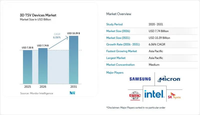
Mordor Intelligence에 따르면 2026년 3D TSV 디바이스 시장 규모는 77억 4,000만 달러로 추정되며, 2025년 73억 달러에서 확대되어 2031년에는 103억 9,000만 달러에 달할 것으로 예측됩니다.
2026년부터 2031년까지의 연평균 성장률(CAGR)은 6.06%에 달할 전망입니다.
본 보고서는 제품 유형(이미징 및 광전자, 메모리, 기타), TSV 기술(Via-Middle, Via-Last, Via-First), 웨이퍼 크기(200mm 이하, 300mm, 450mm), 최종사용자 산업(소비자 가전, 자동차, IT·통신, 기타), 및 지역(아메리카, 유럽, 기타)별로 분류되어 있습니다. 시장 예측은 금액(달러) 기준으로 제시되어 있습니다.
세계 3D TSV 디바이스 시장의 동향 및 인사이트
고성능 컴퓨팅 및 AI 워크로드에 대한 수요 증가
대규모 언어 모델의 훈련은 현재 1조 파라미터를 초과하여, 메모리 계층이 GDDR6를 넘어설 필요가 대두되고 있습니다. SK하이닉스의 12층 적층 HBM4 엔지니어링 샘플은 2.1 Tbit/s의 대역폭을 실현하여 HBM3E에 비해 64% 향상되었으며, GPU 클러스터에 행렬 곱셈의 피크 처리 능력을 위한 여유를 제공하고 있습니다. 2024년에 승인된 JEDEC의 HBM4 표준에서는 2048비트 인터페이스가 규정되어 있으며, 이를 지원할 수 있는 것은 실리콘 관통 비아(TSV) 아키텍처뿐입니다. 마이크론의 2024년 연차 보고서에 따르면, HBM 매출은 2배 이상 증가했으며, 2026년에 생산능력을 확대하기 위해 15억 달러가 계상되었습니다. 삼성이 구리 대 구리 하이브리드 본딩으로 전환함에 따라 비아 저항이 40% 감소하고, 수 GHz 대역의 신호 무결성이 향상되었습니다. 인텔의 ‘Gaudi 3’ 가속기는 실리콘 인터포저 위에 8개의 HBM3E 스택을 통합하고 있으며, 이에 따라 CHIPS법에 기반한 공동 자금 지원 하에 애리조나주와 뉴멕시코주에서 35억 달러 규모의 패키징 시설 확장이 진행되고 있습니다.
데이터센터의 확장이 고대역폭 메모리 채택을 촉진
각 하이퍼스케일러 기업들은 AI 서버를 사상 가장 빠른 속도로 도입하고 있으며, NVIDIA H200 및 AMD MI300X 소켓당 80GB를 초과하는 HBM3를 소비하고 있습니다. TSMC의 CoWoS 라인은 2024년 내내 가동률이 100%를 상회하여, 대만에서 월산 6만 웨이퍼 규모로 확장(투자액 28억 달러)하게 되었습니다. 마이크론의 2024년 5월 투자자용 자료에 따르면, HBM 공급량은 2025년까지 완전히 예약된 상태이며, 이로 인해 평균 판매 가격이 30% 상승할 가능성이 있습니다. 브로드컴(Broadcom)은 TSV 기반 HBM을 각 칩에 통합하여 패키지당 3 Tbit/s 이상의 대역폭을 실현하는 맞춤형 AI ASIC을 출하했습니다. 이러한 동향은 3D TSV 디바이스 시장의 단기적인 가격 결정력을 강화하고 있습니다.
3D TSV 패키지의 높은 단가
TSV 조립은 디바이스 1대당 15-40달러의 추가 비용을 발생시켜, 중급 스마트폰 및 IoT 디바이스의 이익률을 압박하고 있습니다. 에칭 장비는 챔버 1기당 1,500만 달러를 초과하며, 전기도금 시스템에는 추가로 800만 달러의 비용이 듭니다. 암콜(Amcor)의 2024 회계연도 결산 보고서에 따르면, 첨단 패키징 사업의 매출 총이익률은 28%로, 와이어 본딩 수준보다 500 베이시스 포인트 낮습니다. 인증 주기는 장기간에 걸쳐 진행됩니다. ASE의 가오슝 공장 확장 사례에서 알 수 있듯이, 자동차 등급 TSV 패키지에는 1,000시간의 HTOL 시험이 필요하며, 이로 인해 시장 출시까지의 기간이 최대 16주까지 연장될 수 있습니다.
부문별 분석
2025년에는 HBM이 AI 가속기를 위한 사실상 표준 고대역폭 솔루션이 됨에 따라, 메모리 디바이스가 3D TSV 디바이스 시장의 45.92%를 차지했습니다. MEMS 및 센서용 3D TSV 디바이스 시장 규모는 자동차용 레이더 및 관성측정장치의 채택을 반영하여 2031년까지 연평균 성장률(CAGR) 8.57%로 확대될 것으로 예측됩니다. 이미징 및 광전자 분야는 비아 라스트(via-last)형 TSV의 혜택을 받고 있으며, 이를 통해 근적외선 영역에서 90%의 양자 효율을 달성하는 소니의 후면 조사형 센서가 실현되었습니다. LED 공급업체들은 마이크로 LED 디스플레이 구동에 비아 퍼스트(Via-First)형 TSV를 채택하고 있으나, 수율이 60% 미만에 그치고 있어 대규모 도입이 지연되고 있습니다.
그 밖에도 전원 관리 IC나 RF 프론트엔드 등의 제품에서는 인덕턴스를 최소화하기 위해 TSV가 활용되고 있습니다. 퀄컴의 QTM565 밀리미터파 모듈은 1cm³ 패키지에서 10 Gb/s를 달성한 반면, 보쉬의 BMA580 가속도계는 MEMS와 ASIC 다이를 적층함으로써 대기 전류를 1µA로 억제하고 있습니다. 이러한 사례들은 HBM이 수익의 하한선을 확립하고 있음에도 불구하고, 3D TSV 디바이스 산업이 메모리의 범위를 넘어 확장되고 있음을 보여줍니다.
DRAM 및 CIS의 성숙화로 인해 2025년에는 ‘Via-middle’이 매출의 54.15%를 차지했으나, 치플렛 기반 다이가 1µm 미만의 오버레이 정밀도를 필요로 하기 때문에 ‘Via-first’는 연평균 성장률(CAGR) 7.69%로 성장하고 있습니다. 인텔의 Foveros 제품 라인은 현재 36µm 피치를 실현하고 있으며, 2026년까지 10µm을 목표로 하고 있어 1 Tbit/s/mm2를 초과하는 수직 대역폭을 실현할 것입니다.
비아 라스트 방식은 화소 충진율을 95% 이상으로 유지하기 때문에 센서 분야에서 여전히 필수적입니다. 이 세 가지 접근 방식 모두에서 하이브리드 본딩은 상호연결 밀도를 2배로 높이며, 2026년 이후에는 주류가 될 전망으로, 3D TSV 디바이스 시장의 중추로서 TSV의 역할을 확고히 할 것입니다.
지역별 분석
아시아태평양은 2025년에 매출의 42.70%를 차지하며, 연평균 성장률(CAGR) 8.56%로 성장하고 있습니다. 이는 TSMC가 CoWoS 생산능력의 70% 이상을 차지하고 있고, 삼성전자가 HBM 시장에서 45%의 점유율을 확보하고 있으며, SK하이닉스가 이천에서 엔드투엔드 통합을 실현하고 있다는 점이 원동력이 되고 있습니다. 일본에서는 9,200억 엔의 보조금을 통해 2026년까지 구마모토에 첨단 패키징 기술이 도입되어 소니와 덴소에 공급될 전망입니다. 중국의 YMTC는 3D NAND 컨트롤러 적층에 TSV 활용을 목표로 하고 있으나, 수출 규제로 인해 규모 확대 속도가 둔화되고 있습니다. 한국에서는 26조 원의 세제 혜택에 힘입어 SK하이닉스에 50기의 새로운 TSV 에칭 챔버가 도입될 예정입니다. 인도는 2026년부터 구자라트주에서 OSAT 시설을 가동하기 위해 마이크론으로부터 27억 5,000만 달러의 투자를 유치하며, 아시아가 3D TSV 디바이스 시장의 중심지로서의 입지를 공고히 했습니다.
2025년, 북미는 약 34.40%의 점유율을 차지했습니다. 마이크론은 CHIPS법에 따라 뉴욕주와 아이다호주에 HBM 제조 공장을 건설하기 위해 61억 6,500만 달러의 자금을 확보했습니다. 암콜(Amcor)사의 20억 달러 규모 애리조나주 공장은 2027년에 가동을 시작할 예정이며, 자동차 및 방위 산업용 300mm TSV 패키지를 생산할 것입니다. 인텔은 뉴멕시코주 및 애리조나주에서의 확장을 통해 2026년까지 Foveros의 생산능력을 3배로 확대하는 한편, 캐나다는 오타와의 코패키지드 옵틱스(CPO) 시범 라인에 2억 4,000만 캐나다 달러를 투자하고 있습니다. 니어쇼어링의 진전에 따라 텍사스 인스트루먼트와 NXP는 팬아웃 조립을 멕시코로 이전하고 있지만, 이 지역에서는 여전히 TSV용 장비가 부족한 실정입니다.
2025년 시점에서 유럽의 점유율은 약 18.55%였습니다. ST 마이크로일렉트로닉스는 프랑스의 300mm TSV 라인 확장을 위해 29억 유로를 확보했습니다. 인피니온은 드레스덴에서 GaN 파워 디바이스용 비아 미들 TSV 인증을 획득하여 온 저항을 35% 저감했습니다. 프라운호퍼 IZM은 하이브리드 본딩을 통한 선구자 로트에서 0µm의 피치를 실현했으며, 영국은 고온 EV 인버터용 GaN TSV 라인에 5,000만 파운드를 투자했습니다. 남미와 중동 및 아프리카(MEA)의 합산 점유율은 4.35%이지만, 브라질과 아랍에미리트(UAE)는 2027년 이후 생산능력 확충을 시사하고 있습니다.
기타 혜택:
- 엑셀 형식의 시장 예측(ME) 시트
- 3개월간의 애널리스트 지원
자주 묻는 질문
목차
제1장 소개
제2장 조사 방법
제3장 주요 요약
제4장 시장 구도
제5장 시장 규모와 성장 예측
제6장 경쟁 구도
제7장 시장 기회와 향후 전망
KSM 26.08.25According to Mordor Intelligence, 3D TSV devices market size in 2026 is estimated at USD 7.74 billion, growing from 2025 value of USD 7.30 billion with 2031 projections showing USD 10.39 billion, growing at 6.06% CAGR over 2026-2031.
This report is Segmented by Product Type (Imaging and Opto-Electronics, Memory, and More), TSV Technology (Via-Middle, Via-Last, and Via-First), Wafer Size (<=200mm, 300mm, and 450mm), End-User Industry (Consumer Electronics, Automotive, IT and Telecom, and More), and Geography (North America, South America, Europe, and More). The Market Forecasts are Provided in Terms of Value (USD).
Global 3D TSV Devices Market Trends and Insights
Growing Demand for High-Performance Computing and AI Workloads
Large language model training now exceeds 1 trillion parameters, forcing memory hierarchies to move beyond GDDR6. SK Hynix's engineering samples of 12-high HBM4 stacks deliver a 2.1 Tbit/s bandwidth, a 64% increase over HBM3E, providing GPU clusters with headroom for matrix-multiply peaks. JEDEC's HBM4 standard, ratified in 2024, locks in a 2048-bit interface that only through-silicon via architectures can serve. Micron's FY 2024 report indicates HBM revenue more than doubled, with USD 1.5 billion set aside for capacity that ramps in 2026. Samsung's shift to copper-to-copper hybrid bonding trims via resistance by 40%, improving multi-GHz signal integrity. Intel's Gaudi 3 accelerator integrates eight HBM3E stacks on a silicon interposer, prompting a USD 3.5 billion packaging build-out in Arizona and New Mexico under CHIPS Act co-funding.
Expansion of Data Centers Driving High-Bandwidth Memory Adoption
Hyperscalers are deploying AI servers at record velocity, with NVIDIA H200 and AMD MI300X sockets each consuming over 80 GB of HBM3. TSMC's CoWoS lines ran above 100% utilization throughout 2024, triggering a USD 2.8 billion expansion to 60k wafers/month in Taiwan. Micron's May 2024 investor deck indicated that HBM supply was fully booked until 2025, potentially inflating average selling prices by 30%. Broadcom shipped custom AI ASICs that each integrate TSV-based HBM and deliver more than 3 Tbit/s bandwidth per package. These dynamics reinforce the near-term pricing power of the 3D TSV devices market.
High Unit Cost of 3D TSV Packages
A TSV assembly adds USD 15-40 to each device, thereby squeezing margins for mid-tier phones and IoT devices. Etch tools exceed USD 15 million per chamber, while electroplating systems cost another USD 8 million. Amkor's FY 2024 filings reveal advanced-packaging gross margins at 28%, or 500 bps below wire-bond levels. Qualification cycles are long; ASE's Kaohsiung expansion highlighted that automotive-grade TSV packages require 1,000-hour HTOL testing, which can stretch the time-to-market by up to 16 weeks.
Other drivers and restraints analyzed in the detailed report include:
- Rapid Miniaturization in Smartphones and Consumer Electronics
- Chiplet-Based Heterogeneous Integration Architectures
- Thermal-Induced Reliability and Yield Challenges
For complete list of drivers and restraints, kindly check the Table Of Contents.
Segment Analysis
Memory devices captured 45.92% of the 3D TSV devices market in 2025 as HBM became the de facto high-bandwidth solution for AI accelerators. The 3D TSV devices market size for MEMS and sensors is projected to expand at an 8.57% CAGR to 2031, reflecting the adoption of automotive radar and inertial units. Imaging and optoelectronics benefit from via-last TSV, enabling Sony's back-illuminated sensors that reach 90% quantum efficiency in near-IR. LED suppliers are using via-first TSV to power micro-LED displays, although yields below 60% delay mass deployment.
Other products, such as power management ICs and RF front-ends, utilize TSV to minimize inductance. Qualcomm's QTM565 mmWave module hits 10 Gb/s in 1 cm3 packages, while Bosch's BMA580 accelerometer stacks MEMS and ASIC dies for 1 µA standby current. These examples demonstrate how the 3D TSV devices industry expands beyond memory, even as HBM establishes the revenue floor.
Via-middle held 54.15% of the revenue in 2025, due to the maturity of DRAM and CIS; however, via-first is growing at a 7.69% CAGR, as chiplet-based dies demand sub-1 µm overlay accuracy. Intel's Foveros line hits 36 µm pitch today and targets 10 µm by 2026, unlocking >1 Tbit/s/mm2 vertical bandwidth.
Via-last remains critical for sensors, keeping pixel fill factors above 95%. Hybrid bonding across all three approaches doubles interconnect density and will dominate after 2026, cementing TSV's role as the backbone of the 3D TSV devices market.
Complete Report Scope:
- By Product Type
- Imaging and Opto-Electronics
- Memory
- MEMS / Sensors
- LED
- Other Products
- By TSV Technology
- Via-Middle TSV
- Via-Last TSV
- Via-First TSV
- By Wafer Size
- <=200mm
- 300 mm
- 450 mm
- By End-User Industry
- Consumer Electronics
- Automotive
- IT and Telecom
- Healthcare
- Aerospace and Defence
- Other End-User Industries
- By Geography
- North America
- United States
- Canada
- Mexico
- South America
- Brazil
- Argentina
- Rest of South America
- Europe
- Germany
- United Kingdom
- France
- Italy
- Spain
- Russia
- Rest of Europe
- Asia-Pacific
- China
- Japan
- India
- South Korea
- Australia
- Rest of Asia-Pacific
- Middle East and Africa
- Middle East
- Saudi Arabia
- United Arab Emirates
- Turkey
- Rest of Middle East
- Africa
- South Africa
- Nigeria
- Egypt
- Rest of Africa
- Middle East
- North America
Geography Analysis
Asia-Pacific held 42.70% of revenue in 2025 and is expanding at 8.56% CAGR, fueled by TSMC's >70% share of CoWoS capacity, Samsung's 45% grip on HBM, and SK Hynix's end-to-end integration in Icheon. Japan's JPY 920 billion subsidy brings advanced packaging to Kumamoto by 2026, serving Sony and Denso. China's YMTC eyes TSV for 3D NAND controller stacking, but export curbs slow scaling. South Korea's KRW 26 trillion tax incentives underwrite 50 new TSV etch chambers at SK Hynix. India attracts USD 2.75 billion from Micron for a Gujarat OSAT facility starting 2026, sealing Asia's position as the epicenter of the 3D TSV devices market.
North America captured roughly 34.40% in 2025. Micron won USD 6.165 billion to build HBM fabs in New York and Idaho under the CHIPS Act. Amkor's USD 2 billion Arizona plant is scheduled to open in 2027, processing 300 mm TSV packages for the automotive and defense industries. Intel's New Mexico and Arizona expansions triple Foveros capacity by 2026, while Canada invests CAD 240 million in Ottawa's co-packaged optics pilot line. Near-shoring prompts Texas Instruments and NXP to relocate fan-out assembly to Mexico, although TSV tools remain scarce in the region.
Europe owned about 18.55% in 2025. STMicroelectronics secured EUR 2.9 billion to scale 300 mm TSV lines in France. Infineon qualified via-middle TSV for GaN power devices in Dresden, cutting on-resistance by 35%. Fraunhofer IZM has achieved a pitch of 0 µm via pibrid bonding pion lots, and the U.K. invested GBP 50 million in a GaN TSV line for high-temperature EV inverters. South America and MEA together account for 4.35%, though Brazil and the UAE signal post-2027 capacity adds.
- Taiwan Semiconductor Manufacturing Company Limited
- Samsung Electronics Co., Ltd.
- Intel Corporation
- Micron Technology, Inc.
- SK hynix Inc.
- Toshiba Electronic Devices and Storage Corporation
- ASE Technology Holding Co., Ltd.
- Amkor Technology, Inc.
- United Microelectronics Corporation
- STMicroelectronics N.V.
- Broadcom Inc.
- Texas Instruments Incorporated
- GlobalFoundries Inc.
- Advanced Micro Devices, Inc.
- Qualcomm Incorporated
- JCET Group Co., Ltd.
- Powertech Technology Inc.
- Siliconware Precision Industries Co., Ltd.
- Xilinx, Inc. (AMD Adaptive and Embedded Computing Group)
- Pure Storage, Inc.
Additional Benefits:
- The market estimate (ME) sheet in Excel format
- 3 months of analyst support
TABLE OF CONTENTS
1 INTRODUCTION
- 1.1 Study Assumptions and Market Definition
- 1.2 Scope of the Study
2 RESEARCH METHODOLOGY
3 EXECUTIVE SUMMARY
4 MARKET LANDSCAPE
- 4.1 Market Overview
- 4.2 Market Drivers
- 4.2.1 Growing demand for high-performance computing and AI workloads
- 4.2.2 Expansion of data centers driving high-bandwidth memory adoption
- 4.2.3 Rapid miniaturisation in smartphones and consumer electronics
- 4.2.4 Chiplet-based heterogeneous integration architectures
- 4.2.5 Silicon photonics' need for 3D interposer stacking
- 4.2.6 Government subsidies for advanced packaging fabs
- 4.3 Market Restraints
- 4.3.1 High unit cost of 3D TSV packages
- 4.3.2 Thermal-induced reliability and yield challenges
- 4.3.3 Supply-chain bottlenecks for TSV etch and fill tools
- 4.3.4 Stricter environmental rules on TSV chemistries
- 4.4 Industry Value Chain Analysis
- 4.5 Regulatory Landscape
- 4.6 Technological Outlook
- 4.7 Impact of Macroeconomic Factors
- 4.8 Porter's Five Forces Analysis
- 4.8.1 Bargaining Power of Suppliers
- 4.8.2 Bargaining Power of Consumers
- 4.8.3 Threat of New Entrants
- 4.8.4 Intensity of Competitive Rivalry
- 4.8.5 Threat of Substitutes
5 MARKET SIZE AND GROWTH FORECASTS (VALUE)
- 5.1 By Product Type
- 5.1.1 Imaging and Opto-Electronics
- 5.1.2 Memory
- 5.1.3 MEMS / Sensors
- 5.1.4 LED
- 5.1.5 Other Products
- 5.2 By TSV Technology
- 5.2.1 Via-Middle TSV
- 5.2.2 Via-Last TSV
- 5.2.3 Via-First TSV
- 5.3 By Wafer Size
- 5.3.1 <=200mm
- 5.3.2 300 mm
- 5.3.3 450 mm
- 5.4 By End-User Industry
- 5.4.1 Consumer Electronics
- 5.4.2 Automotive
- 5.4.3 IT and Telecom
- 5.4.4 Healthcare
- 5.4.5 Aerospace and Defence
- 5.4.6 Other End-User Industries
- 5.5 By Geography
- 5.5.1 North America
- 5.5.1.1 United States
- 5.5.1.2 Canada
- 5.5.1.3 Mexico
- 5.5.2 South America
- 5.5.2.1 Brazil
- 5.5.2.2 Argentina
- 5.5.2.3 Rest of South America
- 5.5.3 Europe
- 5.5.3.1 Germany
- 5.5.3.2 United Kingdom
- 5.5.3.3 France
- 5.5.3.4 Italy
- 5.5.3.5 Spain
- 5.5.3.6 Russia
- 5.5.3.7 Rest of Europe
- 5.5.4 Asia-Pacific
- 5.5.4.1 China
- 5.5.4.2 Japan
- 5.5.4.3 India
- 5.5.4.4 South Korea
- 5.5.4.5 Australia
- 5.5.4.6 Rest of Asia-Pacific
- 5.5.5 Middle East and Africa
- 5.5.5.1 Middle East
- 5.5.5.1.1 Saudi Arabia
- 5.5.5.1.2 United Arab Emirates
- 5.5.5.1.3 Turkey
- 5.5.5.1.4 Rest of Middle East
- 5.5.5.2 Africa
- 5.5.5.2.1 South Africa
- 5.5.5.2.2 Nigeria
- 5.5.5.2.3 Egypt
- 5.5.5.2.4 Rest of Africa
- 5.5.5.1 Middle East
- 5.5.1 North America
6 COMPETITIVE LANDSCAPE
- 6.1 Market Concentration
- 6.2 Strategic Moves
- 6.3 Market Share Analysis
- 6.4 Company Profiles (includes Global level Overview, Market level overview, Core Segments, Financials as available, Strategic Information, Market Rank/Share for key companies, Products and Services, and Recent Developments)
- 6.4.1 Taiwan Semiconductor Manufacturing Company Limited
- 6.4.2 Samsung Electronics Co., Ltd.
- 6.4.3 Intel Corporation
- 6.4.4 Micron Technology, Inc.
- 6.4.5 SK hynix Inc.
- 6.4.6 Toshiba Electronic Devices and Storage Corporation
- 6.4.7 ASE Technology Holding Co., Ltd.
- 6.4.8 Amkor Technology, Inc.
- 6.4.9 United Microelectronics Corporation
- 6.4.10 STMicroelectronics N.V.
- 6.4.11 Broadcom Inc.
- 6.4.12 Texas Instruments Incorporated
- 6.4.13 GlobalFoundries Inc.
- 6.4.14 Advanced Micro Devices, Inc.
- 6.4.15 Qualcomm Incorporated
- 6.4.16 JCET Group Co., Ltd.
- 6.4.17 Powertech Technology Inc.
- 6.4.18 Siliconware Precision Industries Co., Ltd.
- 6.4.19 Xilinx, Inc. (AMD Adaptive and Embedded Computing Group)
- 6.4.20 Pure Storage, Inc.
7 MARKET OPPORTUNITIES AND FUTURE OUTLOOK
- 7.1 White-space and unmet-need assessment


