

|
시장보고서
상품코드
2114334
원자층 증착(ALD) : 시장 점유율 분석, 업계 동향 및 통계, 성장 예측(2026-2031년)Atomic Layer Deposition - Market Share Analysis, Industry Trends & Statistics, Growth Forecasts (2026 - 2031) |
||||||
 Mordor Intelligence
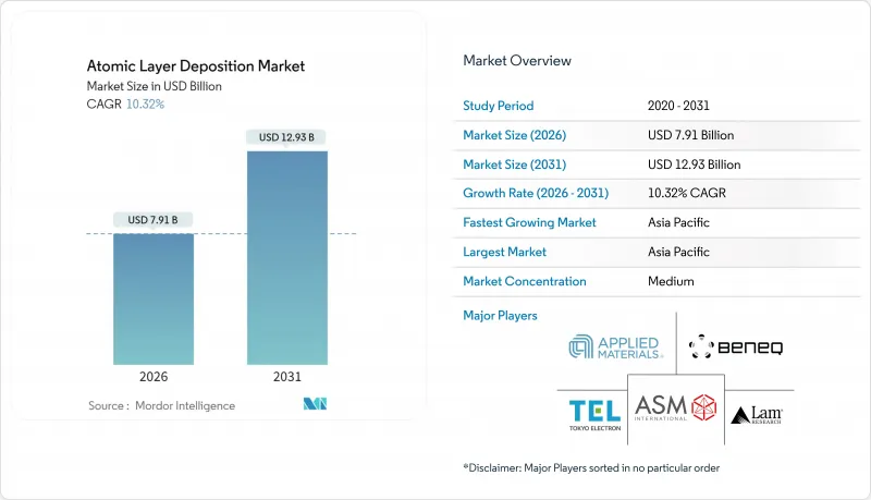
Mordor Intelligence에 의하면, 원자층 증착(ALD) 시장 규모는 2026년에 79억 1,000만 달러에 이르고, 2031년까지 129억 3,000만 달러로 확대되며 예측 기간 중 연평균 복합 성장률(CAGR) 은 10.32%를 나타낼 전망입니다.
본 보고서는 장비 유형(열식 ALD 배치, 플라즈마 강화 ALD 등), 반응기 구성(클러스터형 단일 웨이퍼,스탠드얼론형 배치), 기판 크기(200mm 이하, 300mm, 기타), 성막 화학 물질(산화물, 금속, 기타), 용도(반도체 로직 및 메모리, 첨단 패키징 등) 및 지역별로 분류되어 있습니다. 시장 예측은 금액(달러) 기준으로 제시되어 있습니다.
세계의 원자층 증착(ALD) 시장 동향 및 인사이트
아시아에서 3D NAND 및 DRAM 노드 미세화의 급속한 확대
2025년에는 수직형 NAND의 층 수가 300층을 초과하고, 종횡비 80 : 1을 넘는 조건에서 사이드월의 컨포멀리티를 유지하기 위해 메모리 공장에서는 웨이퍼 1장당 최대 14단계의 ALD 공정을 도입할 수밖에 없게 되었습니다. 또한 DRAM 제조업체들도 커패시터 직경이 18나노미터 미만인 1-베타 구조로 전환했습니다. 이 미세 구조를 누설 없이 채울 수 있는 것은 ALD를 통한 지르코늄 도핑 하프늄 산화물뿐입니다. 삼성은 2025년에 ALD 장비가 메모리 공장 설비 투자의 22%를 차지했다고 밝혔습니다. 이는 3년 전 16%에서 증가한 수치입니다. 중국의 YMTC도 이에 발맞추어 Xtacking 4.0 설계에 ALD 티타늄 질화물 라이너를 추가하고,월10만 웨이퍼 규모의 라인당 1억 2,000만 달러를 추가 투자했습니다. 이러한 투자는 아시아태평양의 리더십을 강화하는 동시에, 적어도 향후 2세대 노드 미세화 과정에서 장비 수요 전망을 더욱 명확하게 하고 있습니다.
게이트 올 어라운드(GAA) 및 고-k 금속 게이트 로직으로의 전환
게이트 올 어라운드(GAA)형 전계 효과 트랜지스터는 채널을 컨포멀한 고-k 유전체로 감싸, 등가 산화막 두께를 0.7나노미터 미만으로 줄입니다. TSMC의 N2 리스크 생산 공정에서는 12사이클의 하프늄 산화물 ALD 스택에 이어 질화 티타늄 워크펑션 금속을 증착하도록 요구하며, 이 모든 공정은 산소 크로스톡을 억제하기 위해 독립된 ALD 챔버 내에서 수행됩니다. 인텔의 18A 노드에서는 접촉 저항을 19% 저감하는 선택적 ALD 코발트 라이너가 추가되었습니다. 삼성의 2세대 3나노미터 공정에서는 ALD의 화학 조성을 최적화하여 계면층을 얇게 만들어 23%의 전력 소비 감소를 실현했습니다. ALD의 사이클 시간은 최대 180초에 달하기도 하지만, 파운드리 각사는 챔버의 병렬 운영을 통해 병목 현상을 완화하고 있으며, 3나노미터 이하의 로직에서 ALD가 필수적인 역할을 하고 있음이 부각되고 있습니다.
전구체 금속공급 부족과 가격 변동
루테늄, 이리듐, 코발트는 주로 남아프리카와 러시아에서 백금족 금속의 일종으로 채굴되며, 그 공급은 지정학적 위험에 노출되어 있습니다. ALD 및 전해조 제조업체들이 제한된 생산량을 놓고 경쟁한 결과, 루테늄 가격은 2024년 트로이 온스당 450달러에서 2025년 말에는 603달러까지 상승했습니다. 각 파운드리 업체들은 펄스 타이밍을 최적화하여 사용량을 줄였지만, 웨이퍼 생산 개시 건수가 계속 증가하고 있어 수요가 효율 개선 효과를 상회하고 있습니다. 대체 화학 조성에 대한 시험이 진행 중이지만, 인증 과정에 2-3년이 소요되므로 변동성이 심한 현물 가격에 대한 노출이 장기화되고 있습니다.
부문별 분석
플라즈마 강화형 장비는 2025년 매출의 38.23%를 차지하며, 이는 배선 및 화합물 반도체를 보호하는 이 장비의 뛰어난 저온 처리 능력을 보여주었습니다. 나노시트 로직 및 3D DRAM에서는 300°C 미만의 처리가 필수적이기 때문에 플라즈마 시스템용 원자층 증착(ALD) 시장 규모는 2031년까지 전체 시장과 동등한 연평균 성장률(CAGR) 10% 가까이 확대될 전망입니다. 열식 ALD로는 적절한 속도로 형성할 수 없는 컨포멀 질화물 및 티타늄 막이 수요의 기반을 이루고 있습니다. 대조적으로, 공간 아키텍처는 특히 플렉서블 기판에서 원자 수준의 정밀도와 선형 속도의 절충을 통해 연평균 성장률(CAGR) 12.41%를 나타낼 전망입니다. WCS 500 플랫폼은 시간당 10m²의 웹을 코팅할 수 있어, 이를 통해 디스플레이 생산 라인은 배치식 챔버에서는 지금까지 불가능했던 택트 타임 목표를 달성할 수 있게 됩니다. 다만, 전구체의 폐기량은 여전히 40% 더 많습니다. 열식 배치형 장치는 플라즈마에 의한 손상을 허용할 수 없는 학술 기관이나 생의학 분야의 생산 라인에서 여전히 사용되고 있지만, 팹이 클러스터 설계로 통합됨에 따라 그 점유율은 해마다 줄어들고 있습니다.
앞으로 하나의 인클로저 내에서 플라즈마 ALD와 원자층 에칭을 결합한 하이브리드 스택이 주목받고 있습니다. 도쿄 일렉트로 ‘Tactras’ 장비는 웨이퍼의 핸드오프 횟수를 줄이고, 개별 모듈에 비해 전반적인 생산성을 18% 향상시킵니다. 이러한 통합 기술을 습득한 공급업체는 팹이 정밀도와 처리량 모두를 추구하는 가운데 시장 점유율을 더욱 확대해 나갈 것입니다. 한편, 배터리 및 디스플레이 제조업체들은 배치 방식과 동등한 균일성을 절반의 비용으로 실현하는 롤-투-롤 설계를 공급업체에 요구하고 있으며, 이는 원자층 증착 시장 내 제품 로드맵의 분화를 시사합니다.
클러스터형 단일 웨이퍼 플랫폼은 2025년 매출의 44.57%를 차지했으며, 로직 팹이 오염 격리에 투자함에 따라 연평균 성장률(CAGR) 11.02%를 유지할 것으로 예측됩니다. 각 웨이퍼가 전용 챔버를 점유하기 때문에 크로스 토크 없이 신속한 화학 조성 변경이 가능하며, 이는 코발트 라이너와 유전체 스택을 교대로 형성할 때 매우 중요합니다. 배치형 리액터의 원자층 증착 시장 점유율은 감소 추세를 보이고 있습니다. 이는 웨이퍼당 비용이 낮다는 장점에도 불구하고, 7나노미터 이하 노드에서 레시피 유연성의 한계를 상쇄할 수 없기 때문입니다. 그럼에도 불구하고, 중국의 구세대 팹에서는 2025년 신규 도입의 38%를 배치형 장비가 차지하고 있으며, 최첨단 로직 반도체를 제외한 분야에서는 자본 효율성이 여전히 결정적인 요인임을 보여줍니다.
공간형 단일 웨이퍼 시스템은 오염 제어와 높은 기계적 처리량을 결합함으로써 기존의 구분을 모호하게 만들고 있습니다. 박막 균일성 문제가 해결된다면, 클러스터 장비가 현재 누리고 있는 프리미엄을 잠식할 가능성이 있습니다. 따라서 공급업체들은 위험을 분산시키고 있습니다. ASM 인터내셔널의 ‘펄서(Pulsar)’ 시리즈는 싱글 웨이퍼 분야에서의 리더십을 유지하는 한편, 이 회사의 새로운 공간형 포트폴리오는 디스플레이 및 배터리 사용자를 대상으로 하고 있습니다. 향후 10년 동안 구매자의 선택은 장비 제조업체가 하나의 모듈식 프레임 내에서 사이클 타임, 박막 품질, 총 소유 비용을 조화시킬 수 있는지 여부에 달려 있을 것입니다.
지역별 분석
아시아태평양은 2025년에 매출 점유율 53.43%를 유지했으며, 2031년까지 연평균 성장률(CAGR) 11.28%로 상승할 것으로 예측됩니다. 대만, 한국, 중국은 300mm 생산 능력의 78%를 합쳐 차지하고 있으며, 장비 제조업체인 도쿄 일렉트로닉과 히타치 하이테크가 이 지역에서의 도입을 가속화하는 현지 조달 가능한 공급망을 제공합니다. 한국의 3D NAND 분야 리더십이 워드라인 배리어 및 차지 트랩 층 수요를 견인하고 있으며, 중국의 웨이퍼 팹 확장으로 인해 성숙 노드용 장비, 이미지 센서 및 전력 관리 집적 회로용 장비가 흡수되고 있습니다. 일본은 장비 수출 및 고체 배터리 라인의 조기 구축으로 혜택을 보고 있습니다. 인도의 100억 달러 규모의 반도체 장려책은 아직 대량 생산형 팹으로 이어지지는 않았지만, 장기적인 수요 가능성을 시사하고 있습니다.
북미는 2위를 차지했습니다. 이는 ‘CHIPS 법’에 따른 390억 달러 규모의 보조금과 인텔, TSMC, 삼성, 마이크론 각사가 발표한 2,000억 달러를 초과하는 팹 투자에 힘입은 결과입니다. 이러한 프로젝트의 웨이퍼 팹 설비 예산 전체 중 ALD 장비가 약 14%를 차지하고 있습니다. 캐나다의 역할은 주로 연구 중심인 반면, 멕시코는 구리 확산 배리어에 ALD 기술을 활용한 첨단 패키징 라인에 주력하고 있습니다.
유럽은 2030년까지 세계 반도체 시장 점유율 20%를 확보하는 것을 목표로 하는 430억 유로(470억 달러) 규모의 ‘EU 칩스법’에 힘입어 성장세를 이어가고 있습니다. 인텔의 마크데부르크 공장과 TSMC의 드레스덴 공장에서는 2026년 이후 양산용 ALD 모듈이 도입될 예정입니다. ST 마이크로일렉트로닉스는 자동차 업계 고객에게 ALD로 보호된 실리콘 카바이드 디바이스를 공급하기 위해 클로르에서 사업을 확장하고 있습니다. 중동 및 아프리카는 여전히 발전 단계에 있으며, 투자 펀드에 의한 시험적인 프로젝트로 제한되어 있습니다.
남미 시장 진출은 학술 연구소에 국한되어 있으며, 산업 분야의 설비 투자는 프런트엔드 제조보다 조립에 중점을 두고 있습니다. 그 결과, 원자층 증착(ALD) 시장은 여전히 고도로 집중되어 있으며, 대만, 한국,중국, 미국, 일본 등 주요 5개국이 2025년 장비 매출의 84%를 차지하고 있습니다. 보조금으로 인해 시장 구도에 약간의 변화가 생길 가능성은 있지만, 확립된 노하우, 공급업체 생태계, 그리고 기존 감가상각 일정에 힘입어 당분간 아시아태평양의 우위는 흔들리지 않을 것입니다.
기타 혜택 :
- 엑셀 형식 시장 예측(ME) 시트
- 3개월간의 애널리스트 지원
자주 묻는 질문
목차
제1장 서론
제2장 조사 방법
제3장 주요 요약
제4장 시장 구도
제5장 시장 규모 및 성장 예측
제6장 경쟁 구도
제7장 시장 기회 및 향후 전망
KTH 26.08.28According to Mordor Intelligence, the atomic layer deposition market size reached USD 7.91 billion in 2026 and is projected to climb to USD 12.93 billion by 2031, reflecting a 10.32% CAGR over the forecast horizon.
This report is Segmented by Equipment Type (Thermal ALD Batch, Plasma-Enhanced ALD, and More), Reactor Configuration (Cluster Single-Wafer, and Stand-Alone Batch), Substrate Size (<=200mm, 300mm, and More), Film Chemistry (Oxide, Metal, and More), Application (Semiconductor Logic and Memory, Advanced Packaging, and More), and Geography. The Market Forecasts are Provided in Terms of Value (USD).
Global Atomic Layer Deposition Market Trends and Insights
Surging 3D NAND And DRAM Node Shrink In Asia
Layer counts in vertical NAND exceeded 300 in 2025, forcing memory fabs to introduce up to 14 ALD steps per wafer to maintain sidewall conformality at aspect ratios above 80:1. DRAM makers also moved to 1-beta structures with capacitor diameters under 18 nanometers, a geometry that only ALD zirconium-doped hafnium oxide can fill without leakage. Samsung disclosed that ALD tools consumed 22% of memory-fab capex in 2025, up from 16% three years earlier. China's YMTC followed suit by adding ALD titanium-nitride liners in its Xtacking 4.0 design, spending an extra USD 120 million per 100 000-wafer-per-month line. These investments reinforce Asia-Pacific's leadership and elevate tool-demand visibility for at least the next two node shrinks.
Transition To Gate-All-Around And High-k Metal Gate Logic
Gate-all-around field-effect transistors wrap the channel with a conformal high-k dielectric, lowering equivalent oxide thickness below 0.7 nanometers. TSMC's N2 risk-production flow calls for a 12-cycle hafnium-oxide ALD stack followed by titanium-nitride work-function metal, all deposited in isolated ALD chambers to curb oxygen cross-talk. Intel's 18A node adds a selective ALD cobalt liner that cuts contact resistance 19%. Samsung's second-generation 3 nanometer flow achieved 23% power gains with a thinner interfacial layer credited to optimized ALD chemistry. Although ALD cycle times can top 180 seconds, foundries are mitigating bottlenecks through parallel chamber counts, underscoring the indispensable role of ALD in sub-3-nanometer logic.
Scarcity And Cost Volatility Of Precursor Metals
Ruthenium, iridium, and cobalt are mined mainly as platinum-group by-products in South Africa and Russia, exposing supply to geopolitical risk. Ruthenium rose from USD 450 per troy ounce in 2024 to USD 603 by end-2025 as both ALD and electrolyzer builders chased limited output. Foundries squeezed usage through smarter pulse timing, but wafer starts keep rising, so demand outpaces efficiency gains. Substitute chemistries are in trial, yet qualification cycles last two to three years, prolonging exposure to volatile spot prices.
Other drivers and restraints analyzed in the detailed report include:
- Rapid Adoption Of Mini and Micro-LED Backplanes
- EV Battery Solid-State Electrolyte Coatings Demand
- Throughput Limitations Versus High-Volume Foundry Targets
For complete list of drivers and restraints, kindly check the Table Of Contents.
Segment Analysis
Plasma-enhanced tools generated 38.23% of 2025 revenue, a testament to their low-temperature capability that shields interconnects and compound semiconductors. The atomic layer deposition market size for plasma systems is set to rise at nearly the overall 10% CAGR through 2031 as nanosheet logic and 3D DRAM mandate sub-300 °C processing. Conformal nitride and titanium films, unachievable by thermal ALD at reasonable rates, anchor demand. In contrast, spatial architectures will post a 12.41% CAGR by trading atomic-level accuracy for linear speed, especially on flexible substrates. The WCS 500 platform coats 10 m2 webs hourly, allowing display lines to meet takt-time goals previously impossible with batch chambers, though precursor waste remains 40% higher. Thermal batch tools linger in academia and biomedical lines where plasma damage is prohibitive, but their share shrinks each year as fabs consolidate around cluster designs.
Looking ahead, hybrid stacks combining plasma ALD and atomic-layer etching inside one chassis are gaining traction. Tokyo Electron's Tactras tool reduces wafer handoffs and lifts overall productivity 18% compared with discrete modules. Suppliers that master such integration will capture incremental wallet share as fabs chase both precision and throughput. Meanwhile, battery and display producers are pushing vendors for roll-to-roll designs that equal batch uniformity at half the cost, hinting at divergent product roadmaps inside the atomic layer deposition market.
Cluster single-wafer platforms delivered 44.57% of 2025 revenue and should sustain an 11.02% CAGR as logic fabs pay for contamination isolation. Each wafer occupies its own chamber, allowing rapid chemistry changes without cross-talk, critical when alternating cobalt liners with dielectric stacks. The atomic layer deposition market share for batch reactors is sliding because their lower cost per wafer cannot offset limited recipe agility at sub-7 nanometer nodes. Still, trailing-edge fabs in China procured batch tools for 38% of 2025 adds, illustrating that capital efficiency remains a deciding factor outside cutting-edge logic.
Spatial single-wafer systems blur the historical split by combining contamination control with higher mechanical throughput. If film-uniformity hurdles are solved, they could erode the premium now enjoyed by cluster tools. Suppliers are therefore hedging bets: ASM International's Pulsar line maintains single-wafer leadership, while its new spatial portfolio targets display and battery users. Over the decade, buyer choice will hinge on whether tool makers can harmonize cycle time, film quality, and cost of ownership inside one modular frame.
Complete Report Scope:
- By Equipment Type
- Thermal ALD (Batch)
- Plasma-Enhanced ALD (PEALD)
- Spatial ALD
- Roll-to-Roll / Sheet-to-Sheet ALD
- Atomic Layer Etching (ALE)-Enabled Tools
- By Reactor Configuration
- Cluster (Single-Wafer)
- Stand-Alone Batch
- By Substrate Size
- <=200mm
- 300 mm
- >=450mm Pilot Lines
- By Film Chemistry
- Oxide Films
- Nitride and Oxy-Nitride Films
- Metal Films, Co, Ru, Ti, Al, Cu
- Fluoride and Sulfide Films
- By Application
- Semiconductor Logic and Memory
- Advanced Packaging and Heterogeneous Integration
- Power and Optoelectronics, SiC, GaN, LEDs
- Energy Devices, Li-Ion, Solid-State, Fuel Cells
- Biomedical and Implant Surface Functionalization
- Automotive Sensors and ADAS
- By Geography
- North America
- United States
- Canada
- Mexico
- South America
- Brazil
- Argentina
- Rest of South America
- Europe
- United Kingdom
- Germany
- France
- Spain
- Italy
- Rest of Europe
- Asia-Pacific
- China
- India
- Japan
- Australia
- South Korea
- Rest of Asia-Pacific
- Middle East
- Saudi Arabia
- United Arab Emirates
- Turkey
- Rest of Middle East
- Africa
- South Africa
- Kenya
- Rest of Africa
- North America
Geography Analysis
Asia-Pacific retained 53.43% revenue share in 2025 and is forecast to rise at an 11.28% CAGR through 2031. Taiwan, South Korea, and China jointly held 78% of 300 millimeter capacity, while tool makers Tokyo Electron and Hitachi High-Tech provide an indigenous supply chain that accelerates regional adoption. South Korea's 3D NAND leadership drives word-line barrier and charge-trap layer demand, and China's wafer-fab build-out absorbs equipment for mature nodes, image sensors, and power management integrated circuits. Japan benefits from equipment exports and early roll-outs of solid-state battery lines. India's USD 10 billion semiconductor incentive has yet to translate into high-volume fabs but signals potential longer-term demand.
North America ranked second, propelled by USD 39 billion in CHIPS Act subsidies and over USD 200 billion in announced fab investments from Intel, TSMC, Samsung, and Micron. ALD tools account for about 14% of total wafer-fab equipment budgets across these projects. Canada's role is largely research-oriented, while Mexico focuses on advanced packaging lines using ALD for copper diffusion barriers.
Europe follows on the strength of the EUR 43 billion (USD 47 billion) EU Chips Act that aims for 20% global semiconductor share by 2030. Intel's Magdeburg fab and TSMC's Dresden plant will deploy volume ALD modules after 2026. STMicroelectronics expands in Crolles to supply automotive customers with ALD-protected silicon-carbide devices. The Middle East and Africa remain nascent, limited to exploratory projects by investment funds.
South America's participation is confined to academic labs; industrial capex centers on assembly rather than front-end fabrication. Consequently, the atomic layer deposition market remains highly concentrated, with the top five countries Taiwan, South Korea, China, the United States, and Japan capturing 84% of 2025 equipment revenue. Subsidies may shift the mix at the margin, yet entrenched know-how, supplier ecosystems, and existing depreciation schedules ensure Asia-Pacific's primacy for the foreseeable future.
- ASM International N.V.
- Applied Materials Inc.
- Tokyo Electron Limited
- Lam Research Corporation
- Veeco Instruments Inc.
- Oxford Instruments plc
- Beneq Oy
- Picosun Oy
- Entegris Inc.
- Kurt J. Lesker Company
- Hitachi High-Tech Corporation
- Ulvac Inc.
- Aixtron SE
- SENTECH Instruments GmbH
- CVD Equipment Corporation
- Forge Nano Inc.
- ALD NanoSolutions Inc.
- Lotus Applied Technology
- LPE S.p.A.
- SVT Associates
- Arradiance LLC
- Beneq R2R (Service Business)
Additional Benefits:
- The market estimate (ME) sheet in Excel format
- 3 months of analyst support
TABLE OF CONTENTS
1 INTRODUCTION
- 1.1 Study Assumptions and Market Definition
- 1.2 Scope of the Study
2 RESEARCH METHODOLOGY
3 EXECUTIVE SUMMARY
4 MARKET LANDSCAPE
- 4.1 Market Overview
- 4.2 Market Drivers
- 4.2.1 Surging 3-D NAND and DRAM Node Shrink in Asia
- 4.2.2 Transition to Gate-All-Around (GAA) and High-K Metal Gate Logic
- 4.2.3 Rapid Adoption of Mini/Micro-LED Backplanes
- 4.2.4 EV Battery Solid-State Electrolyte Coatings Demand
- 4.2.5 Medical Implant Nano-Coatings for Improved Bio-Compatibility
- 4.2.6 Government-Funded Pilot-Line Investments, EU Chips Act, CHIPS and Science Act
- 4.3 Market Restraints
- 4.3.1 Scarcity and Cost Volatility of Precursor Metals, Ru, Ir, Co
- 4.3.2 Throughput Limitations vs High-Volume Foundry Targets
- 4.3.3 Competing Spatial CVD for OLED Encapsulation
- 4.3.4 Stringent EHS Regulations on Fluorinated Plasma By-Products
- 4.4 Industry Value Chain Analysis
- 4.5 Regulatory Landscape
- 4.6 Technological Outlook
- 4.7 Porter's Five Forces Analysis
- 4.7.1 Bargaining Power of Suppliers
- 4.7.2 Bargaining Power of Buyers
- 4.7.3 Threat of New Entrants
- 4.7.4 Threat of Substitutes
- 4.7.5 Intensity of Competitive Rivalry
- 4.8 Impact of Macroeconomic Factors on the Market
5 MARKET SIZE AND GROWTH FORECASTS (VALUE)
- 5.1 By Equipment Type
- 5.1.1 Thermal ALD (Batch)
- 5.1.2 Plasma-Enhanced ALD (PEALD)
- 5.1.3 Spatial ALD
- 5.1.4 Roll-to-Roll / Sheet-to-Sheet ALD
- 5.1.5 Atomic Layer Etching (ALE)-Enabled Tools
- 5.2 By Reactor Configuration
- 5.2.1 Cluster (Single-Wafer)
- 5.2.2 Stand-Alone Batch
- 5.3 By Substrate Size
- 5.3.1 <=200mm
- 5.3.2 300 mm
- 5.3.3 >=450mm Pilot Lines
- 5.4 By Film Chemistry
- 5.4.1 Oxide Films
- 5.4.2 Nitride and Oxy-Nitride Films
- 5.4.3 Metal Films, Co, Ru, Ti, Al, Cu
- 5.4.4 Fluoride and Sulfide Films
- 5.5 By Application
- 5.5.1 Semiconductor Logic and Memory
- 5.5.2 Advanced Packaging and Heterogeneous Integration
- 5.5.3 Power and Optoelectronics, SiC, GaN, LEDs
- 5.5.4 Energy Devices, Li-Ion, Solid-State, Fuel Cells
- 5.5.5 Biomedical and Implant Surface Functionalization
- 5.5.6 Automotive Sensors and ADAS
- 5.6 By Geography
- 5.6.1 North America
- 5.6.1.1 United States
- 5.6.1.2 Canada
- 5.6.1.3 Mexico
- 5.6.2 South America
- 5.6.2.1 Brazil
- 5.6.2.2 Argentina
- 5.6.2.3 Rest of South America
- 5.6.3 Europe
- 5.6.3.1 United Kingdom
- 5.6.3.2 Germany
- 5.6.3.3 France
- 5.6.3.4 Spain
- 5.6.3.5 Italy
- 5.6.3.6 Rest of Europe
- 5.6.4 Asia-Pacific
- 5.6.4.1 China
- 5.6.4.2 India
- 5.6.4.3 Japan
- 5.6.4.4 Australia
- 5.6.4.5 South Korea
- 5.6.4.6 Rest of Asia-Pacific
- 5.6.5 Middle East
- 5.6.5.1 Saudi Arabia
- 5.6.5.2 United Arab Emirates
- 5.6.5.3 Turkey
- 5.6.5.4 Rest of Middle East
- 5.6.6 Africa
- 5.6.6.1 South Africa
- 5.6.6.2 Kenya
- 5.6.6.3 Rest of Africa
- 5.6.1 North America
6 COMPETITIVE LANDSCAPE
- 6.1 Market Concentration
- 6.2 Strategic Initiatives and JV Analysis
- 6.3 Market Share Analysis
- 6.4 Company Profiles (includes Global-Level Overview, Market-Level Overview, Core Segments, Financials as Available, Strategic Information, Market Rank/Share, Products and Services, Recent Developments)
- 6.4.1 ASM International N.V.
- 6.4.2 Applied Materials Inc.
- 6.4.3 Tokyo Electron Limited
- 6.4.4 Lam Research Corporation
- 6.4.5 Veeco Instruments Inc.
- 6.4.6 Oxford Instruments plc
- 6.4.7 Beneq Oy
- 6.4.8 Picosun Oy
- 6.4.9 Entegris Inc.
- 6.4.10 Kurt J. Lesker Company
- 6.4.11 Hitachi High-Tech Corporation
- 6.4.12 Ulvac Inc.
- 6.4.13 Aixtron SE
- 6.4.14 SENTECH Instruments GmbH
- 6.4.15 CVD Equipment Corporation
- 6.4.16 Forge Nano Inc.
- 6.4.17 ALD NanoSolutions Inc.
- 6.4.18 Lotus Applied Technology
- 6.4.19 LPE S.p.A.
- 6.4.20 SVT Associates
- 6.4.21 Arradiance LLC
- 6.4.22 Beneq R2R (Service Business)
7 MARKET OPPORTUNITIES AND FUTURE OUTLOOK
- 7.1 White-Space and Unmet-Need Assessment


