|
시장보고서
상품코드
2114453
박막 증착 : 시장 점유율 분석, 업계 동향 및 통계, 성장 예측(2026-2031년)Thin Layer Deposition - Market Share Analysis, Industry Trends & Statistics, Growth Forecasts (2026 - 2031) |
||||||
 Mordor Intelligence
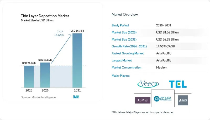
Mordor Intelligence에 의하면, 박막 증착 시장 규모는 2025년에 249억 3,000만 달러, 2026년 285억 6,000만 달러에서 2031년에는 563억 5,000만 달러에 이를 것으로 예측되며, 예측 기간(2026-2031년) CAGR은 14.56%를 기록할 전망입니다.
본 보고서는 증착 기술(물리적 기상 증착, 화학적 기상 증착, 기타),장비 유형(인라인 생산 라인, 기타), 증착 재료 유형(금속 및 합금, 산화물, 질화물 및 탄화물, 화합물 및 2차원 소재), 최종 이용 산업(광학 디스플레이, 기타), 지역별로 분류되어 있습니다. 시장 예측은 달러 기준 금액으로 제시되어 있습니다.
세계 박막 증착 시장 동향 및 인사이트
칩렛·3D-IC 아키텍처에 따른 초컨포멀 상호 연결 박막에 대한 수요 증가
이종 통합으로 인해 상호 연결 설계가 변화하고 있으며, 보이드가 없는 높은 종횡비 비아를 덮는 배리어 층과 시드 층이 요구되고 있습니다. 대만 반도체 제조 회사(TSMC)의 CoWoS-S는종횡비 20:1을 가진 스루 실리콘 비아를 사용하여 로직과 고대역폭 메모리를 적층하고 있는데, 이 비아에서는 구리 확산 제어를 위해 원자층 증착법(ALD)으로 증착된 티타늄 질화물이 필요합니다. 인텔(Intel)의 2024년판 ‘Foveros Direct’ 기술에서는 범프 피치가 25μm로 축소됨에 따라, 화학 기상 성장법으로는 달성하기 어려운 95%의 스텝 커버리지를 가진 코발트 시드 층으로의 전환이 시급해지고 있습니다. 삼성 파운더리는 2027년까지 2μm 라인 앤 스페이스 재배선을 목표로 하고 있으며, 이를 위해서는 루테늄 라이너의 플라즈마 강화 원자층 증착법이 필수적입니다. 각 장비 공급업체의 수주가 급증하고 있으며, 어플라이드 머티리얼즈는 2024 회계연도에 첨단 패키징용 증착 장비 매출이 전년 대비 38% 증가했다고 보고했습니다. 산업 컨소시엄은 유기 인터포저와 호환되는 300°C 이하의 공정을 가능하게 하기 위해, 시클로펜타디에닐계 루테늄 등의 새로운 전구체 도입을 추진하고 있습니다.
페로브스카이트 탠덤 태양전지 제조의 급속한 규모 확대
페로브스카이트-실리콘 탠덤 태양전지는 2024년에 변환 효율 33%의 대기를 돌파하며, 파일럿 라인 개발이 급증했습니다. 옥스포드 포토볼타익스는 브란덴부르크주에서 200MW 규모의 생산을 시작했으며, 슬롯 다이 공정을 이용한 페로브스카이트 층과 PECVD 공정을 이용한 산화주석 전자 수송막을 결합하고 있습니다. Longi는 Meyer Burger와 제휴하여 페로브스카이트를 TOPCon 모듈에 통합함으로써 2026년까지 30%의 효율 달성을 목표로 하고 있습니다. 미국 에너지부는 패시베이션 층의 처리량을 10배 높이는 것을 목표로, 공간 원자층 증착(SALD) 프로젝트에 4,000만 달러를 지원했습니다. 벤처 캐피탈이 유입되고 있습니다. 스위프트 솔라(Swift Solar)는 롤-투-롤 방식의 스퍼터링을 통한 투명 전도체를 채택한 경량 탠덤 패널의 상용화를 위해 2,700만 달러를 조달했습니다. 국제에너지기구(IEA)는 증착 장비의 가동률이 90% 이상을 유지하고, 재료 이용률이 70%를 초과한다는 전제 하에 2030년까지 탠덤 패널의 생산 능력이 50GW에 달할 것으로 예측했습니다.
헬륨 및 고순도 전구체공급 부족으로 인한 운영 비용(OPEX) 증가
미국 연방 헬륨 비축량의 고갈로 인해 현물 가격은 2023년 m3당 8달러에서 2024년 중반에는 16달러로 급등했습니다. 300mm 팹에서는 연간 1,500만 m³의 헬륨을 소비하고 있으며, 램 리서치(Lam Research)는 2024 회계연도에 1,200만 달러의 추가 헬륨 비용이 발생했다고 밝혔습니다. 폐쇄형 회수 시스템은 공정 가스의 95%를 회수할 수 있지만, 1기당 도입 비용은 300만 달러가 듭니다. 고유전율(High-k) 전구체도 유사한 공급 부족에 직면해 있으며, 사염화하프늄의 생산 능력이 3개사로 한정되어 있어 리드타임이 8주에서 20주로 늘어났습니다. 2024년 8월 중국이 시행한 지르코늄 화합물 수출 규제로 인해 공급이 더욱逼迫해졌으며, 각 팹(fab) 업체들은 듀얼 소스 계약을 체결할 수밖에 없게 되었고, 그 결과 단위 비용이 18% 상승했습니다.
부문별 분석
2025년, 화학 기상 증착(CVD)은 박막 증착 시장에서 50.74%의 시장 점유율을 차지했습니다. 이는 유전체, 폴리실리콘, 텅스텐을 높은 증착 속도로 증착할 수 있는 범용성을 반영한 것입니다. 원자층 증착(ALD)은 옹스트롬 단위의 두께 제어가 필요한 3nm 이하 트랜지스터 게이트에 대한 수요에 힘입어 연평균 성장률(CAGR) 17.18%를 나타낼 것으로 예측됩니다. ALD가 차지하는 박막 증착 시장 규모는 2025년에 92억 달러에 달할 것으로 예상되며, 2031년까지 2배로 증가할 것으로 전망됩니다. 물리 기상 증착(PVD)은 성숙한 노드의 알루미늄 배선 분야에서 여전히 확고한 입지를 차지하고 있지만, 램 리서치(Lam Research)의 ‘SABRE 3D’와 같은 하이브리드 공정에서는 이온화 PVD와 ALD 배리어 층을 결합하여 계면 저항을 25% 저감하고 있습니다. 신기술인 폴리머 분자층 증착은 플렉서블 전자 기기의 기능적 선택지를 넓혀주고, 아직 시작 단계이긴 하지만 빠르게 성장하는 수익원을 창출하고 있습니다.
게이트 올 어라운드(GAA) 나노 시트로 전환하는 로직 파운드리에서는 이전 세대의 8단계에 비해 최대 15단계의 ALD 공정이 채택되고 있습니다. 인텔의 18A 노드는 종횡비 5:1의 채널을 하프늄 산화물과 티타늄 질화물의 적층체가 감싸는 구조를 통해 이러한 도약을 상징합니다. CVD는 100nm/min의 증착 속도로 웨이퍼 비용을 낮게 억제할 수 있기 때문에 얕은 트렌치 절연(STI) 및 층간 유전체 갭 필에서 여전히 지배적인 위치를 유지하고 있습니다. 종횡비가 높아짐에 따라, 각 공급업체들은 전환 시기를 늦추기 위해 고밀도 플라즈마 CVD 및 고리플로우 라이너 개발을 추진하고 있습니다. 선택적 증착은 활발한 연구 분야이며, Tokyo Electron Ltd.의 ‘Tactras Vigus’ 장치는 ALE와 ALD를 인시투 계측과 결합하여 ±0.5nm의 자기 정합 접점을 실현하고 있어, 차기 로직 사이클에서 리소그래피 공정을 생략할 가능성이 있습니다.
배치식 로는 2025년 매출의 56.05%를 차지하며, 범용 로직, 태양전지, 광학 코팅 부문에서 웨이퍼당 낮은 비용으로 높은 평가를 받고 있습니다. 한편, 롤-투-롤(R2R) 및 공간 ALD 장비는 연평균 성장률(CAGR) 16.36%로 성장을 지속하고, 있으며, 이는 웹 기반 연속 공정이 필요한 연성 OLED 디스플레이, 배터리용 분리막, 양면형 태양전지 모듈로의 전환을 반영하고 있습니다. 싱글 웨이퍼 클러스터는 진공 통합 챔버를 통한 입자 제어가 필수적인 첨단 로직 및 3D NAND 부문에서 여전히 필수적입니다. 공간 ALD 장비용 박막 증착 시장 규모는 2025년에 28억 달러였으나, 처리량에 대한 우려가 완화됨에 따라 2031년까지 60억 달러에 달할 것으로 예측됩니다.
Beneq의 공간 ALD 가동률은 2024년에 85%를 넘어섰으며, 대량 도입에 대한 기존 장벽이 해소되었습니다. 애플라이드 머티리얼즈의 ‘올림피아’는 공간 ALD 모듈과 PVD 모듈을 공유 이송 시스템에 통합하여, TOPCon 패시베이션에서 시간당 1,200장의 웨이퍼 처리를 실현함으로써 배치 리액터에 비해 생산성을 15배 향상시켰습니다. 폰 알덴네(Von Ardenne)사의 롤-투-롤형 마그네트론 스퍼터링은 폴리이미드 위에 산화 인듐-아연을 분당 20m의 속도로 증착하여, 굽힘 반경 3mm의 폴더블 스마트폰 구현을 가능하게 하고 있습니다. Canon·아넬바의 ‘ENAS’ 플랫폼은 스퍼터링 출력 제어에 머신러닝을 통합하여, 300mm 웨이퍼의 박막 두께 편차를 약 1.5%로 저감함으로써 10nm 이하의 구리 배선 공정 윈도우를 완화하고 있습니다.
지역별 분석
아시아태평양은 TSMC, 삼성, 여러 중국계 파운드리 업체들의 제조 능력 확대에 힘입어 2025년 매출의 44.78%를 차지했습니다. 이 지역의 설비 투자액은 360억 달러를 넘어섰으며, TSMC가 그 대부분을 차지했고, 그중 25%가 증착 장비에 투자되었습니다. 중국에서는 AMEC의 장비가 SMIC의 14nm 라인에 도입됨에 따라 2024년 장비 자급률이 28%로 상승했습니다. 한국 정부의 20조 원 규모 보조금 지원으로 SK하이닉스의 HBM 양산 확대가 뒷받침되었으며, 이 회사는 120대의 ALD 리액터를 발주했습니다. 일본의 Rapidus 얼라이언스는 IBM과 IMEC의 전문 지식을 활용하여 게이트-투-게이트 기술 연구 개발을 위해 30대의 장비를 구입했습니다.
북미에서는 ‘CHIPS 법’에 따라 회복의 조짐이 보입니다. 인텔과 TSMC 피닉스는 2026년까지 300대 이상의 리액터를 도입할 예정이며, 한편 마이크론의 뉴욕 DRAM 공장에서는 커패시터 유전체 형성을 위해 80대의 ALD 장비를 사용할 계획입니다. 애플라이드 머티리얼즈는 이러한 급증하는 수요에 대응하기 위해 몬태나주에 40억 달러 규모의 공장 건설에 착수하고, 20만 제곱피트 규모의 클린룸을 증설했습니다. 유럽은 파워 반도체와 화합물 반도체에 주력하고 있습니다. 인피니언(Infineon)의 드레스덴 공장과 TSMC의 유럽 합작 회사는 실리콘 카바이드 및 구리 배선용으로 60대의 PVD 및 CVD 장비를 추가로 도입할 예정입니다. 사우디아라비아의 20GW 입찰과 같은 중동의 태양광 발전 메가 프로젝트에서는 폰 알덴네(Von Ardenne)와 싱귤러스(Singularus)로부터 대면적 스퍼터 라인이 발주되어, 이로 인해 해당 지역 시장 점유율이 확대되고 있습니다. 남미와 아프리카는 여전히 발전 단계에 있지만, 아시아의 생산 능력에 의존하는 범용 태양광 제품 수입을 통해 간접적인 혜택을 보고 있습니다. 지역 연구 기관들은 유연 센서용 롤-투-롤 ALD 기술을 연구하고 있으며, 2030년 이후 장비 판매의 소폭 증가로 이어질 수 있는 현지 노하우를 축적하고 있습니다. 이러한 신흥 지역을 종합해 보면 현재 매출의 5% 미만을 차지할 뿐이지만, 비용 곡선이 하락하면 장기적인 성장 기회를 가져다줄 것입니다.
기타 혜택
- 엑셀 형식 시장 예측(ME) 시트
- 3개월간의 애널리스트 지원
자주 묻는 질문
목차
제1장 서론
제2장 조사 방법
제3장 주요 요약
제4장 시장 구도
제5장 시장 규모와 성장 예측
제6장 경쟁 구도
제7장 시장 기회와 향후 전망
LSH 26.08.26According to Mordor Intelligence, the thin layer deposition market size was valued at USD 24.93 billion in 2025 and estimated to grow from USD 28.56 billion in 2026 to reach USD 56.35 billion by 2031, at a CAGR of 14.56% during the forecast period (2026-2031).
This report is Segmented by Deposition Technology (Physical Vapor Deposition, Chemical Vapor Deposition, and More), Equipment Type (In-Line Production Lines, and More), Material Type Deposited (Metals and Alloys, Oxides, Nitrides and Carbides, Compound and 2-D Materials), End-Use Industry (Optics and Displays, and More), and Geography. The Market Forecasts are Provided in Terms of Value in USD.
Global Thin Layer Deposition Market Trends and Insights
Chiplet And 3D-IC Architectures Intensify The Need For Ultra-Conformal Interconnect Films
Heterogeneous integration is changing interconnect design, demanding barrier and seed layers that cover high-aspect-ratio vias without voids. Taiwan Semiconductor Manufacturing Company's CoWoS-S stacks logic with high-bandwidth memory using 20:1 aspect-ratio through-silicon vias that require titanium nitride deposited by atomic layer deposition for copper diffusion control. Intel's 2024 Foveros Direct technology reduced bump pitch to 25 μm, forcing a shift to cobalt seed layers with 95% step coverage that chemical vapor deposition struggles to achieve. Samsung Foundry aims for 2 μm line-and-space redistribution by 2027, which will rely on plasma-enhanced atomic layer deposition of ruthenium liners. Tool vendors saw orders surge; Applied Materials reported 38% year-over-year growth in advanced-packaging deposition tools in fiscal 2024. Industry consortia are pushing new precursors, such as cyclopentadienyl-based ruthenium, to enable sub-300 °C processing compatible with organic interposers.
Rapid Scale-Up of Perovskite Tandem Solar Cell Manufacturing
Perovskite-silicon tandems surpassed the 33% efficiency mark in 2024, sparking a surge in the development of pilot lines. Oxford Photovoltaics commenced 200 MW production in Brandenburg, utilizing slot-die perovskite layers in combination with PECVD tin oxide electron transport films. Longi has partnered with Meyer Burger to integrate perovskites into TOPCon modules, aiming for 30% efficiency by 2026. The U.S. Department of Energy has granted USD 40 million to spatial atomic layer deposition projects, aiming for 10X throughput gains in passivation layers. Venture capital is flowing: Swift Solar raised USD 27 million to commercialize lightweight tandem panels that rely on roll-to-roll sputtered transparent conductors. The International Energy Agency forecasts 50 GW of tandem capacity by 2030, provided that deposition tools maintain uptime above 90% and material utilization exceeds 70%.
Helium And High-Purity Precursor Supply Crunch Inflates OPEX
The U.S. Federal Helium Reserve depletion drove spot prices from USD 8 m-3 in 2023 to USD 16 m-3 by mid-2024. A 300 mm fab consumes 15 million m3 annually, and Lam Research disclosed USD 12 million extra helium costs in fiscal 2024. Closed-loop recovery systems recapture 95% of process gas but cost USD 3 million per installation. High-k precursors face similar strain; hafnium tetrachloride capacity is restricted to three makers, stretching lead times from 8 to 20 weeks. China's August 2024 export controls on zirconium compounds further tightened the supply, prompting fabs to enter into dual-source agreements that increase unit costs by 18%.
Other drivers and restraints analyzed in the detailed report include:
- Spatial ALD And Roll-To-Roll PVD Breakthroughs Slashing Cost Per Nanometer
- Government CHIPS-Like Incentives Boosting Domestic Deposition Tool CAPEX
- Escalating Scope-3 Carbon-Reporting Mandates Penalize Vacuum Processes
For complete list of drivers and restraints, kindly check the Table Of Contents.
Segment Analysis
Chemical vapor deposition held a 50.74% market share in the thin layer deposition market in 2025, reflecting its versatility in depositing dielectrics, polysilicon, and tungsten at high rates. Atomic layer deposition is forecast to grow at a 17.18% CAGR, driven by the need for sub-3 nm transistor gates, which require angstrom-scale thickness control. The thin layer deposition market size allocated to ALD reached USD 9.2 billion in 2025 and is expected to double by 2031. Physical vapor deposition remains entrenched for aluminum interconnects at mature nodes; however, hybrid flows, such as Lam Research's SABRE 3D, merge ionized PVD with ALD barriers to reduce interface resistance by 25%. The emerging molecular layer deposition of polymers broadens the functional options for flexible electronics, adding a nascent but fast-growing revenue stream.
Logic foundries moving to gate-all-around nanosheets employ up to 15 ALD steps, versus eight in the prior generation. Intel's 18A node epitomizes this leap with hafnium oxide and titanium nitride stacks wrapped around channels with 5:1 aspect ratios. CVD maintains dominance in shallow trench isolation and inter-layer dielectric gap-fill because 100 nm min-1 rates keep wafer costs down. As aspect ratios increase, suppliers are advancing high-density plasma CVD and high-reflow liners to delay switchover points. Selective deposition is an active frontier: Tokyo Electron's Tactras Vigus tool combines ALE and ALD with in-situ metrology, achieving +-0.5 nm self-aligned contacts that could eliminate lithography steps in the next logic cycle.
Batch furnaces delivered 56.05% of 2025 revenue, prized for their low cost per wafer in commodity logic, solar, and optical coatings. However, roll-to-roll and spatial tools registered a 16.36% CAGR, reflecting a pivot toward flexible OLED displays, battery separators, and bifacial solar modules that need web-based continuous processing. Single-wafer clusters remain indispensable in advanced logic and 3D NAND, where vacuum-integrated chambers ensure particle control. The thin layer deposition market size for spatial ALD equipment was USD 2.8 billion in 2025 and is expected to reach USD 6 billion by 2031 as throughput concerns ease.
Beneq's spatial ALD uptime moved past 85% in 2024, removing a historical barrier to mass adoption. Applied Materials' Olympia integrates spatial ALD and PVD modules in a shared transfer system, achieving 1,200 wafers per hour for TOPCon passivation, a 15X productivity increase over batch reactors. Roll-to-roll magnetron sputtering at Von Ardenne coats indium zinc oxide on polyimide at a rate of 20 m min-1, enabling foldable phones with a bend radius of 3 mm. Canon Anelva's ENAS platform integrates machine learning into sputter power control, reducing thickness variation to around 1.5% on 300 mm wafers, thereby easing process windows for sub-10 nm copper interconnects.
Complete Report Scope:
- By Deposition Technology
- Physical Vapor Deposition (PVD)
- Chemical Vapor Deposition (CVD)
- Atomic Layer Deposition (ALD)
- Hybrid / Emerging Techniques
- By Equipment Type
- Batch Systems
- Single-wafer Cluster Tools
- Roll-to-Roll / Spatial Systems
- In-line Production Lines
- By Material Type Deposited
- Metals and Alloys
- Oxides
- Nitrides and Carbides
- Compound / 2-D Materials
- By End-Use Industry
- Semiconductors and Micro-electronics
- Photovoltaics and Energy Storage
- Medical Devices and Healthcare
- Optics and Displays
- Tools and Industrial Components
- By Geography
- North America
- United States
- Canada
- Mexico
- South America
- Brazil
- Argentina
- Rest of South America
- Europe
- Germany
- United Kingdom
- France
- Italy
- Spain
- Russia
- Rest of Europe
- Asia Pacific
- China
- Japan
- India
- South Korea
- Australia
- Rest of Asia Pacific
- Middle East and Africa
- Middle East
- Saudi Arabia
- United Arab Emirates
- Turkey
- Rest of Middle East
- Africa
- South Africa
- Nigeria
- Egypt
- Rest of Africa
- Middle East
- North America
Geography Analysis
The Asia Pacific region controlled 44.78% of 2025 revenue, driven by fabrication expansions at TSMC, Samsung, and multiple Chinese foundries. Capital spending in the region exceeded USD 36 billion, with TSMC alone accounting for a significant portion, 25% of which was earmarked for deposition equipment. China increased its equipment self-sufficiency to 28% in 2024, as AMEC tools were integrated into SMIC's 14 nm lines. South Korean subsidies of KRW 20 trillion supported SK Hynix's HBM ramps that ordered 120 ALD reactors. Japan's Rapidus alliance purchased 30 tools for gate-to-gate R&D, leveraging expertise from IBM and IMEC.
North America is rebounding under the CHIPS Act. Intel and TSMC Phoenix will install more than 300 reactors by 2026, while Micron's New York DRAM fab plans to use 80 ALD tools for capacitor dielectrics. Applied Materials broke ground on a USD 4 billion factory in Montana to serve this surge, adding 200,000 square feet of cleanrooms. Europe focuses on power and compound semiconductors; Infineon's Dresden fab and TSMC European JV add 60 PVD and CVD tools for silicon carbide and copper interconnects. Middle East solar mega-projects, such as Saudi Arabia's 20 GW tender, order large-area sputter lines from Von Ardenne and Singulus, thereby extending the regional share. South America and Africa remain nascent, but they benefit indirectly from commodity solar imports that rely on Asian manufacturing capacity. Regional research institutes explore roll-to-roll ALD for flexible sensors, building local know-how that could translate into modest equipment sales post-2030. Collectively, these emerging regions represent under 5% of current revenue, yet they provide a long tail of opportunity once cost curves fall.
- Applied Materials Inc.
- Lam Research Corporation
- Tokyo Electron Limited
- ASM International NV
- Veeco Instruments Inc.
- Aixtron SE
- Advanced Micro-Fabrication Equipment Inc. (AMEC)
- IHI Hauzer Techno Coating B.V.
- Oerlikon Balzers
- CVD Equipment Corporation
- Canon Anelva Corporation
- ULVAC Inc.
- Picosun Oy
- Beneq Group Oy
- Kurt J. Lesker Company
- Mustang Vacuum Systems LLC
- Optorun Co., Ltd.
- Von Ardenne GmbH
- Singulus Technologies AG
- Platit AG
Additional Benefits:
- The market estimate (ME) sheet in Excel format
- 3 months of analyst support
TABLE OF CONTENTS
1 INTRODUCTION
- 1.1 Study Assumptions and Market Definition
- 1.2 Scope of the Study
2 RESEARCH METHODOLOGY
3 EXECUTIVE SUMMARY
4 MARKET LANDSCAPE
- 4.1 Market Overview
- 4.2 Market Drivers
- 4.2.1 Chiplet And 3D-IC Architectures Intensify Need for Ultra-Conformal Interconnect Films
- 4.2.2 Rapid Scale-Up of Perovskite Tandem Solar Cell Manufacturing
- 4.2.3 Spatial ALD And Roll-To-Roll PVD Breakthroughs Slashing Cost / Nm
- 4.2.4 Government CHIPS-Like Incentives Boosting Domestic Deposition Tool CAPEX
- 4.2.5 AI-Powered Predictive Maintenance Reducing Deposition Tool Downtime
- 4.2.6 Emergence Of Biodegradable Implant Coatings in Med-Tech
- 4.3 Market Restraints
- 4.3.1 Helium And High-Purity Precursor Supply Crunch Inflates OPEX
- 4.3.2 Escalating Scope-3 Carbon-Reporting Mandates Penalise Vacuum Processes
- 4.3.3 Skilled Vacuum-Process Talent Shortage Lengthens Fab Ramps
- 4.3.4 Competition From Additive Manufacturing of Functional Layers
- 4.4 Impact of Macroeconomic Factors
- 4.5 Industry Value Chain Analysis
- 4.6 Regulatory Landscape
- 4.7 Technological Outlook
- 4.8 Porter's Five Forces Analysis
- 4.8.1 Bargaining Power of Buyers
- 4.8.2 Bargaining Power of Suppliers
- 4.8.3 Threat of New Entrants
- 4.8.4 Threat of Substitute Products
- 4.8.5 Intensity of Competitive Rivalry
5 MARKET SIZE AND GROWTH FORECASTS (VALUE)
- 5.1 By Deposition Technology
- 5.1.1 Physical Vapor Deposition (PVD)
- 5.1.2 Chemical Vapor Deposition (CVD)
- 5.1.3 Atomic Layer Deposition (ALD)
- 5.1.4 Hybrid / Emerging Techniques
- 5.2 By Equipment Type
- 5.2.1 Batch Systems
- 5.2.2 Single-wafer Cluster Tools
- 5.2.3 Roll-to-Roll / Spatial Systems
- 5.2.4 In-line Production Lines
- 5.3 By Material Type Deposited
- 5.3.1 Metals and Alloys
- 5.3.2 Oxides
- 5.3.3 Nitrides and Carbides
- 5.3.4 Compound / 2-D Materials
- 5.4 By End-Use Industry
- 5.4.1 Semiconductors and Micro-electronics
- 5.4.2 Photovoltaics and Energy Storage
- 5.4.3 Medical Devices and Healthcare
- 5.4.4 Optics and Displays
- 5.4.5 Tools and Industrial Components
- 5.5 By Geography
- 5.5.1 North America
- 5.5.1.1 United States
- 5.5.1.2 Canada
- 5.5.1.3 Mexico
- 5.5.2 South America
- 5.5.2.1 Brazil
- 5.5.2.2 Argentina
- 5.5.2.3 Rest of South America
- 5.5.3 Europe
- 5.5.3.1 Germany
- 5.5.3.2 United Kingdom
- 5.5.3.3 France
- 5.5.3.4 Italy
- 5.5.3.5 Spain
- 5.5.3.6 Russia
- 5.5.3.7 Rest of Europe
- 5.5.4 Asia Pacific
- 5.5.4.1 China
- 5.5.4.2 Japan
- 5.5.4.3 India
- 5.5.4.4 South Korea
- 5.5.4.5 Australia
- 5.5.4.6 Rest of Asia Pacific
- 5.5.5 Middle East and Africa
- 5.5.5.1 Middle East
- 5.5.5.1.1 Saudi Arabia
- 5.5.5.1.2 United Arab Emirates
- 5.5.5.1.3 Turkey
- 5.5.5.1.4 Rest of Middle East
- 5.5.5.2 Africa
- 5.5.5.2.1 South Africa
- 5.5.5.2.2 Nigeria
- 5.5.5.2.3 Egypt
- 5.5.5.2.4 Rest of Africa
- 5.5.5.1 Middle East
- 5.5.1 North America
6 COMPETITIVE LANDSCAPE
- 6.1 Market Concentration
- 6.2 Strategic Moves
- 6.3 Market Share Analysis
- 6.4 Company Profiles (includes Global level Overview, Market level overview, Core Segments, Financials as available, Strategic Information, Market Rank/Share for key companies, Products and Services, and Recent Developments)
- 6.4.1 Applied Materials Inc.
- 6.4.2 Lam Research Corporation
- 6.4.3 Tokyo Electron Limited
- 6.4.4 ASM International NV
- 6.4.5 Veeco Instruments Inc.
- 6.4.6 Aixtron SE
- 6.4.7 Advanced Micro-Fabrication Equipment Inc. (AMEC)
- 6.4.8 IHI Hauzer Techno Coating B.V.
- 6.4.9 Oerlikon Balzers
- 6.4.10 CVD Equipment Corporation
- 6.4.11 Canon Anelva Corporation
- 6.4.12 ULVAC Inc.
- 6.4.13 Picosun Oy
- 6.4.14 Beneq Group Oy
- 6.4.15 Kurt J. Lesker Company
- 6.4.16 Mustang Vacuum Systems LLC
- 6.4.17 Optorun Co., Ltd.
- 6.4.18 Von Ardenne GmbH
- 6.4.19 Singulus Technologies AG
- 6.4.20 Platit AG
7 MARKET OPPORTUNITIES AND FUTURE OUTLOOK
- 7.1 White-space and Unmet-need Assessment