

|
시장보고서
상품코드
2115045
에피택시 장비 시장 : 시장 점유율 분석, 업계 동향 및 통계, 성장 예측(2026-2031년)Epitaxy Equipment - Market Share Analysis, Industry Trends & Statistics, Growth Forecasts (2026 - 2031) |
||||||
 Mordor Intelligence
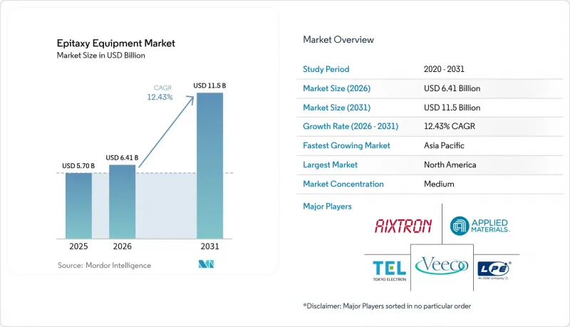
에 의하면, 에피택시 장비 시장 규모는 2025년에 57억 달러로 평가되었고, 2026년 64억 1,000만 달러에서 2031년까지 115억 달러에 이를 것으로 예측되며, 예측 기간(2026-2031년) CAGR은 12.43%를 나타낼 전망입니다.
본 보고서는 기술별(금속 유기 화학 기상 증착법(MOCVD), 수소화물 기상 에피택시법(HVPE) 등), 용도별(포토닉스, 반도체 등), 웨이퍼 크기별(4인치 이하, 6인치, 8인치, 12인치, 12인치 이상과), 소재별(III-V계(GaAs, InP), GaN, SiC 등), 그리고 지역별로 분류되어 있습니다. 시장 전망은 금액(달러) 기준으로 제시되어 있습니다.
세계의 에피택시 장비 시장 동향 및 인사이트
고휘도 LED에 대한 수요 증가
프리미엄 디스플레이 및 자동차 조명 분야에서 MicroLED와 mini-LED가 채택됨에 따라, San'an Optoelectronics와 같은 LED 제조업체들은 다중 시스템 MOCVD 수주를 확보하고 있습니다. 처리량 향상을 위해서는 6인치 및 8인치 웨이퍼 전체의 결함 밀도 저감이 필수적이며, 이로 인해 Veeco사의 Lumina 플랫폼 수주 잔고는 높은 수준을 유지하고 있습니다. 자동차용 주간 주행등 및 어댑티브 빔 헤드램프 역시 더 높은 광속을 필요로 하고 있으며, 그 결과 GaN 층의 균일성에 관한 에피택시 사양이 상향 조정되고 있습니다. 이러한 요인들이 결합되어 3-4년 주기의 예측 가능한 장비 교체 주기가 형성되었으며, 이는 중기적인 출하 전망을 견고하게 하고 있습니다.
EV 파워트레인의 급속한 전동화
자동차 제조업체들은 800V 아키텍처로의 전환을 추진하고 있으며, 이에 따라 1,600°C 이상에서 성장시킨 에피택셜 층이 필요한 실리콘 카바이드(SiC) MOSFET 및 다이오드의 채택이 가속화되고 있습니다. 도쿄 일렉트론의 고온 CVD 장비 수주는 보쉬가 앨라배마주의 SiC 생산 라인을 위해 CHIPS법에 근거한 2억 2,500만 달러의 보조금을 확보함에 따라 증가했습니다. SiC 기판이 150mm에서 200mm로 전환되는 추세에 따라 전 세계 팹에서 신규 장비에 대한 투자와 개조 키트 도입이 필수적입니다. 파워 모듈의 수율은 마이크로파이프 밀도나 도핑 드리프트에 매우 민감하기 때문에 디바이스 제조업체는 수개월에 걸친 공정 레시피 공동 개발을 거친 후에야 주문을 하기 때문에 수익 인식은 장기화되지만, 그와 동시에 확고한 도입 기반이 구축되고 있습니다.
리액터 설계에 따른 복잡성
팹에서 듀얼 머티리얼 및 300mm 챔버에 대한 수요가 높아지는 가운데, 전산 유체 역학(CFD) 모델에서는 층류 가스 흐름과 급격한 온도 구배를 동시에 충족시켜야 하므로 연구 개발 주기가 장기화되고 있습니다. 그 결과, 공급업체들은 멀티존 히터, 전동식 인젝터 플레넘, 인시추 분광 타원도계를 통합하고 있으며, 이로 인해 부품표(BOM) 비용과 소프트웨어 검증 비용이 상승하고 있습니다. 이러한 기술적 장벽은 수익 실현을 지연시켜 후발 기업의 진입 장벽을 높이고 있습니다.
부문 분석
금속 유기 화학 기상 증착(MOCVD)은 LED 및 GaN 파워 디바이스 분야에서 확고한 입지를 바탕으로 2025년에 에피택시 장비 시장 점유율의 46.73%를 차지했습니다. 이 부문의 규모가 크기 때문에 대규모 재설계를 거치지 않고도 웨이퍼 크기를 단계적으로 확대할 수 있어 재주문이 지속되고 있습니다. 한편, 원격 플라즈마 CVD는 저온 처리를 통해 취약한 기판에 적용하거나 보다 정밀한 계면 제어가 가능하기 때문에 연평균 성장률(CAGR) 13.35%를 나타낼 것으로 예측됩니다. RPCVD 장비의 에피택시 장비 시장 규모는 2031년까지 15억 9,000만 달러에 달할 것으로 예측됩니다. MBE(분자선 에피택시)와 수소화물 기상 에피택시는 여전히 틈새 분야에 머물러 있지만, 전자는 초고순도 헤테로 구조, 후자는 두꺼운 GaN 기판의 제조에 각각 적합합니다. 한편, HT-CVD는 두께 20μm를 초과하는 SiC 층 형성 분야에서 주류를 이루고 있습니다. 모든 플랫폼에서 공급업체들은 미래 기술 노드에 대응하기 위한 전략으로, 다중 소재 대응의 유연성을 강점으로 내세우고 있습니다.
두 번째 경쟁 초점은 고도의 공정 제어 스택에 있습니다. Tier 1 팹에서는 폐쇄 루프 방식의 방사율 보정이 적용된 온도 측정 및 머신러닝을 통한 고장 감지를 점점 더 강력하게 요구하고 있으며, 이러한 기능은 MOCVD 및 RPCVD 아키텍처에 후속 적용하기가 가장 용이합니다. 그 결과, 평균 판매 가격은 판매량 증가율을 웃도는 속도로 상승하고 있으며, 엔트리 레벨의 중국산 장비가 LED 하위 부문에 넘쳐나는 상황에서도 이익률을 끌어올리고 있습니다. 오픈 플랫폼 소프트웨어 생태계 또한 차별화 요인으로 부상하고 있으며, 이를 통해 팹은 벤더에 관계없이 하드웨어 간에 레시피를 이식할 수 있어 인증 주기를 단축할 수 있게 됩니다.
2025년 매출의 52.10%는 화합물 반도체 소자 제조가 차지할 것으로 보이며, 그 원동력은 RF 증폭기, LiDAR용 VCSEL 및 포토닉스용 트랜시버였습니다. 그러나 가장 빠른 성장을 보이고 있는 것은 전기차용 인버터 및 통신용 전원에 사용되는 광대역 갭 소재로, 연평균 13.52%의 성장률을 보이고 있습니다. 광대역 갭 용도를 위한 에피택시 장비 시장 규모는 2025년에 22억 8,000만 달러에 달했으며, 2031년까지 48억 8,000만 달러를 넘어설 가능성이 있습니다. 포토닉스 분야, 특히 인듐 인화물(InP) PIC는 하이퍼스케일 데이터센터의 광통신 기술의 혜택을 받고 있으며, 코히런트(Coherent)사가 텍사스 주 거점에서 InP 생산량을 3배로 확대한 것이 그 증거입니다. MEMS 파운드리 시장은 규모는 작지만, 압력 센서 및 RF 필터용 맞춤형 에피택셜 스택에 의존하고 있으며, 꾸준하고 전문성이 높은 장비의 틈새 시장을 개척하고 있습니다.
최종 용도의 사례 다변화로 인해 장비 제조업체는 동일한 팹 부지 내에서 SiC, GaN, InP 간에 구성을 변경할 수 있는 모듈형 반응기를 공급할 수밖에 없게 되었습니다. 이러한 적응성을 통해 설비 투자 예산을 급격한 수요 변동으로부터 보호할 수 있습니다. 동시에, 장비 벤더와 화학약품 공급업체간의 제휴를 통해 전구체의 유동 역학을 공동으로 최적화하고, 박막의 화학량론비를 개선하는 한편, GaN 수직 트랜지스터와 같은 새로운 디바이스 아키텍처의 실현을 목표로 하고 있습니다.
지역별 분석
북미는 텍사스주, 애리조나주, 뉴욕주 북부에 밀집된 클러스터에 힘입어 2025년에도 매출 점유율 43.25%를 유지했습니다. ‘CHIPS법’에 따른 자금은 그린필드 팹과 브라운필드 업그레이드 모두에 투입되어, 국내 에피택시 능력에 대한 장기적인 수요를 뒷받침하고 있습니다. 예를 들어, 코히런트(Coherent)의 셔먼 캠퍼스에서는 AI용 광 링크 수요에 대응하기 위해 InP 소자의 생산량을 3배로 늘렸습니다. 정부 계약에 포함된 현지 조달 규정에 따라 조달이 현지 공급업체에 편중되어 있으며, 환율 변동이 수출 경쟁력을 약화시키고 있음에도 불구하고 수주 파이프라인을 강화하고 있습니다.
아시아태평양은 2031년까지 연평균 성장률(CAGR)이 15.22%로 가장 빠르게 성장하는 시장입니다. HC SemiTek 등 중국의 LED 제조업체들은 이미 MOCVD 장비 도입 대수를 2,500대 이상으로 늘려 생산량 면에서 주도적인 위치를 확립하고 있습니다. 동시에, 한국의 주요 메모리 기업들은 CXL 포토닉스 및 HBM 전력 공급을 위한 화합물 반도체 로드맵에 투자하며 이 지역의 잠재 시장을 확대되고 있습니다. 도쿄 일렉트로ンの 2025년 1분기 매출이 6,545억 엔에 달한 것은 업스트림 벤더에 대한 파급 효과를 여실히 보여주고 있습니다.
유럽에서는 자동차의 전동화와 견고한 항공우주 공급망 구축에 주력하고 있습니다. ‘유럽 칩 법’에 기반한 프로그램을 통해 독일과 스웨덴의 SiC 에피택셜 팹에 보조금이 투입되는 한편, 프랑스의 연구 기관에서는 레이더 및 위성 페이로드를 위한 200mm GaN-on-Si 생산 라인의 시범 운영이 진행되고 있습니다. 현지 환경 규제에 따라 지구 온난화 지수가 낮은 공정 가스의 채택이 가속화되고 있으며, 유럽의 팹에서는 개량형 배기가스 처리 모듈의 도입이 진행되고 있습니다. 이 지역은 생산량 면에서는 다른 지역에 뒤처지고 있지만, 높은 이익률을 자랑하는 특수 장비나 양자 컴퓨팅용 소재에 특화된 연구용 MBE 시스템 분야에서 우위를 점하고 있습니다.
기타 혜택 :
- 엑셀 형식 시장 예측(ME) 시트
- 3개월간 애널리스트 지원
자주 묻는 질문
목차
제1장 서론
제2장 조사 방법
제3장 주요 요약
제4장 시장 구도
제5장 시장 규모 및 성장 예측
제6장 경쟁 구도
제7장 시장 기회 및 향후 전망
AJY 26.08.28According to Mordor Intelligence, the epitaxy equipment market size was valued at USD 5.7 billion in 2025 and estimated to grow from USD 6.41 billion in 2026 to reach USD 11.5 billion by 2031, at a CAGR of 12.43% during the forecast period (2026-2031).
This report is Segmented by Technology (Metal-Organic Chemical Vapor Deposition (MOCVD), Hydride Vapor Phase Epitaxy (HVPE), and More), Application (Photonics, Semiconductors, and More), Wafer Size (Less Than or Equal To 4-Inch, 6-Inch, 8-Inch, 12-Inch, and Greater Than 12-Inch), Material (III-V (GaAs, Inp), Gan, Sic and Others), and Geography. The Market Forecasts are Provided in Terms of Value (USD).
Global Epitaxy Equipment Market Trends and Insights
Increasing Demand for High-Brightness LEDs
MicroLED and mini-LED adoption in premium displays and automotive lighting causes LED makers such as San'an Optoelectronics to book multi-system MOCVD orders. Throughput upgrades must coincide with lower defect density across 6- and 8-inch wafers, keeping Veeco's Lumina platform backlog elevated. Automotive daytime-running lamps and adaptive-beam headlamps also require higher luminous flux, which in turn pushes epitaxy specifications for GaN layer uniformity. These combined forces translate into a predictable equipment-replacement cycle every three to four years, fortifying mid-term shipment trajectories.
Rapid Electrification of Powertrains in EVs
Automakers migrate to 800 V architectures, accelerating silicon-carbide MOSFET and diode uptake that demands epitaxial layers grown at >=1,600 °C. Tokyo Electron's high-temperature CVD tool bookings rose in tandem with Bosch securing USD 225 million in CHIPS Act grants for Alabama SiC lines. The move from 150 mm to 200 mm SiC substrates compels both new-tool investments and retrofit kits across global fabs. Because power-module yields are hypersensitive to micropipe density and doping drift, device makers award purchase orders only after months of process-recipe co-engineering, extending revenue recognition yet building an entrenched installed base.
Complexities Associated With Reactor Design
As fabs request dual-material or 300 mm chambers, computational-fluid-dynamics models must reconcile laminar gas flow with sharp temperature gradients, lengthening R&D cycles. Suppliers therefore integrate multi-zone heaters, motorized injector plenums, and in-situ spectroscopic ellipsometry, driving up bill-of-materials and software validation costs. These engineering hurdles defer revenue and raise the entry barrier for latecomers.
Other drivers and restraints analyzed in the detailed report include:
- Expansion of 5G/6G Compound-Semiconductor Front-End Modules
- Government Incentives for SiC/GaN Capacity Build-Out
- Volatile Prices and Supply of Specialty Precursors
For complete list of drivers and restraints, kindly check the Table Of Contents.
Segment Analysis
Metal-organic chemical vapor deposition occupied 46.73% of the epitaxy equipment market share in 2025 on the back of its entrenched position in LED and GaN power devices. The segment's scale enables incremental wafer-size increases without catastrophic redesign, sustaining repeat orders. Remote-plasma CVD, though, is projected to post a 13.35% CAGR as lower-temperature processing opens doors to fragile substrates and tighter interface control. The epitaxy equipment market size for RPCVD tools is expected to reach USD 1.59 billion by 2031. MBE and hydride vapor-phase epitaxy remain niche, favored for ultra-pure heterostructures and thick GaN substrates, respectively, while HT-CVD dominates SiC layers exceeding 20 µm thickness. Across all platforms, suppliers position multi-material flexibility as a hedge against future technology nodes.
A second competitive angle revolves around advanced process-control stacks. Tier-one fabs increasingly insist on closed-loop emissivity-corrected pyrometry and machine-learning fault detection, features most readily retrofitted to MOCVD and RPCVD architectures. Consequently, average selling prices rise faster than unit volumes, cushioning margins even as entry-level Chinese tools crowd the LED subsegment. Open-platform software ecosystems emerge as another differentiator, enabling fabs to port recipes across vendor hardware and thus shorten qualification cycles.
Compound-semiconductor device manufacturing captured 52.10% of 2025 revenue, driven by RF amplifiers, LiDAR VCSELs, and photonics transceivers. Yet the fastest uplift stems from wide-bandgap materials used in electric-vehicle inverters and telecom power supplies, advancing 13.52% annually. The epitaxy equipment market size for wide-bandgap applications stood at USD 2.28 billion in 2025 and could surpass USD 4.88 billion by 2031. Photonics lines, especially indium-phosphide PICs, benefit from hyperscale data-center optics, evidenced by Coherent tripling InP output at its Texas site. MEMS foundries, though smaller, rely on custom epitaxial stacks for pressure sensors and RF filters, carving a steady yet specialized equipment niche.
The diversity of end-use cases forces equipment makers to supply modular reactors configurable between SiC, GaN, and InP within the same fab footprint. Such adaptability protects capex budgets from sudden demand shifts. Concurrently, partnerships between tool vendors and chemical suppliers aim to co-optimize precursor flow dynamics, improving film stoichiometry and unlocking new device architectures such as GaN vertical transistors.
Complete Report Scope:
- By Technology
- Metal-Organic Chemical Vapor Deposition (MOCVD)
- Hydride Vapor Phase Epitaxy (HVPE)
- High-Temperature Chemical Vapor Deposition (HT-CVD)
- Molecular Beam Epitaxy (MBE)
- Remote-Plasma CVD (RPCVD)
- By Application
- Photonics
- Semiconductors
- Wide-Bandgap Materials
- Micro-Electro-Mechanical Systems (MEMS)
- Others
- By Wafer Size
- Less than or Equal to 4-inch
- 6-inch
- 8-inch
- 12-inch
- Greater than 12-inch
- By Material
- III-V (GaAs, InP)
- GaN
- SiC
- Others
- By Geography
- North America
- United States
- Canada
- Mexico
- South America
- Brazil
- Argentina
- Rest of South America
- Europe
- Germany
- United Kingdom
- France
- Italy
- Spain
- Russia
- Rest of Europe
- Asia-Pacific
- China
- Japan
- India
- South Korea
- South-East Asia
- Rest of Asia-Pacific
- Middle East and Africa
- Middle East
- Saudi Arabia
- United Arab Emirates
- Turkey
- Rest of Middle East
- Africa
- South Africa
- Nigeria
- Rest of Africa
- Middle East
- North America
Geography Analysis
North America preserved a 43.25% revenue share in 2025, supported by dense clusters in Texas, Arizona, and upstate New York. CHIPS Act disbursements flow to both greenfield fabs and brownfield upgrades, anchoring long-term demand for domestic epitaxy capacity. Coherent's Sherman campus, for instance, tripled InP device output to meet AI optical-link demand. Local sourcing rules embedded in government contracts tilt procurement toward resident suppliers, bolstering order pipelines even as exchange-rate swings temper export competitiveness.
Asia-Pacific represents the fastest-growing theater with a 15.22% CAGR through 2031. Chinese LED houses such as HC SemiTek accumulate MOCVD install bases that already exceed 2,500 reactors, driving unit-volume leadership. Simultaneously, South Korean memory giants invest in compound-semiconductor roadmaps for CXL photonics and HBM power delivery, widening the regional addressable market. Tokyo Electron's net sales climb to YEN 654.5 billion in Q1 2025 underscores the pull-through effect on upstream tool vendors.
Europe concentrates on automotive electrification and resilient aerospace supply chains. Programs under the European Chips Act channel subsidies to SiC epi fabs in Germany and Sweden, while French institutes pilot 200 mm GaN-on-Si lines for radar and satellite payloads. Local environmental regulations expedite adoption of low-global-warming-potential process gases, prompting European fabs to specify upgraded abatement modules. Although the region trails in unit volumes, it excels in high-margin specialty tools and research-grade MBE systems tailored for quantum-computing materials.
- Aixtron SE
- Applied Materials, Inc.
- Tokyo Electron Limited
- Veeco Instruments Inc.
- LPE S.p.A.
- NuFlare Technology, Inc. (Toshiba Electronic Devices and Storage Corp.)
- II-VI Incorporated (Coherent Corp.)
- Intelligent Epitaxy Technology, Inc.
- DOWA Electronics Materials Co., Ltd.
- Siltronic AG
- RIBER S.A.
- Taiyo Nippon Sanso Corporation
- Chengdu Alight Optoelectronics Technology Co., Ltd.
- Advanced Epi Materials and Devices UK Ltd.
- NAURA Technology Group Co., Ltd.
- Shenzhen Topraysolar Co., Ltd.
- Suzhou Nano Epitaxy Inc.
- VEECO-Suzhou (CMI Suzhou)
- Jiangsu J-PEC Technology Co., Ltd.
- SkyWater Technology Foundry
Additional Benefits:
- The market estimate (ME) sheet in Excel format
- 3 months of analyst support
TABLE OF CONTENTS
1 INTRODUCTION
- 1.1 Study Assumptions and Market Definition
- 1.2 Scope of the Study
2 RESEARCH METHODOLOGY
3 EXECUTIVE SUMMARY
4 MARKET LANDSCAPE
- 4.1 Market Overview
- 4.2 Market Drivers
- 4.2.1 Increasing demand for high-brightness LEDs
- 4.2.2 Rapid electrification of powertrains in EVs
- 4.2.3 Expansion of 5G/6G compound-semiconductor front-end modules
- 4.2.4 Government incentives for SiC/GaN capacity build-out
- 4.2.5 Adoption of gallium-oxide (B-Ga2O3) devices
- 4.2.6 Transition to 8- and 12-inch GaN-on-Si epitaxy lines
- 4.3 Market Restraints
- 4.3.1 Complexities associated with reactor design
- 4.3.2 Volatile prices and supply of specialty precursors
- 4.3.3 Lengthy tool qualification cycles at IDMs and foundries
- 4.3.4 High capex for next-gen high-temperature reactors
- 4.4 Industry Supply Chain Analysis
- 4.5 Regulatory Landscape
- 4.6 Technological Outlook
- 4.7 Impact of Macroeconomic Factors
- 4.8 Porter's Five Forces Analysis
- 4.8.1 Threat of New Entrants
- 4.8.2 Bargaining Power of Buyers/Consumers
- 4.8.3 Bargaining Power of Suppliers
- 4.8.4 Threat of Substitute Products
- 4.8.5 Intensity of Competitive Rivalry
5 MARKET SIZE AND GROWTH FORECASTS (VALUE)
- 5.1 By Technology
- 5.1.1 Metal-Organic Chemical Vapor Deposition (MOCVD)
- 5.1.2 Hydride Vapor Phase Epitaxy (HVPE)
- 5.1.3 High-Temperature Chemical Vapor Deposition (HT-CVD)
- 5.1.4 Molecular Beam Epitaxy (MBE)
- 5.1.5 Remote-Plasma CVD (RPCVD)
- 5.2 By Application
- 5.2.1 Photonics
- 5.2.2 Semiconductors
- 5.2.3 Wide-Bandgap Materials
- 5.2.4 Micro-Electro-Mechanical Systems (MEMS)
- 5.2.5 Others
- 5.3 By Wafer Size
- 5.3.1 Less than or Equal to 4-inch
- 5.3.2 6-inch
- 5.3.3 8-inch
- 5.3.4 12-inch
- 5.3.5 Greater than 12-inch
- 5.4 By Material
- 5.4.1 III-V (GaAs, InP)
- 5.4.2 GaN
- 5.4.3 SiC
- 5.4.4 Others
- 5.5 By Geography
- 5.5.1 North America
- 5.5.1.1 United States
- 5.5.1.2 Canada
- 5.5.1.3 Mexico
- 5.5.2 South America
- 5.5.2.1 Brazil
- 5.5.2.2 Argentina
- 5.5.2.3 Rest of South America
- 5.5.3 Europe
- 5.5.3.1 Germany
- 5.5.3.2 United Kingdom
- 5.5.3.3 France
- 5.5.3.4 Italy
- 5.5.3.5 Spain
- 5.5.3.6 Russia
- 5.5.3.7 Rest of Europe
- 5.5.4 Asia-Pacific
- 5.5.4.1 China
- 5.5.4.2 Japan
- 5.5.4.3 India
- 5.5.4.4 South Korea
- 5.5.4.5 South-East Asia
- 5.5.4.6 Rest of Asia-Pacific
- 5.5.5 Middle East and Africa
- 5.5.5.1 Middle East
- 5.5.5.1.1 Saudi Arabia
- 5.5.5.1.2 United Arab Emirates
- 5.5.5.1.3 Turkey
- 5.5.5.1.4 Rest of Middle East
- 5.5.5.2 Africa
- 5.5.5.2.1 South Africa
- 5.5.5.2.2 Nigeria
- 5.5.5.2.3 Rest of Africa
- 5.5.5.1 Middle East
- 5.5.1 North America
6 COMPETITIVE LANDSCAPE
- 6.1 Market Concentration
- 6.2 Strategic Moves
- 6.3 Market Share Analysis
- 6.4 Company Profiles (includes Global level Overview, Market level overview, Core Segments, Financials as available, Strategic Information, Market Rank/Share for key companies, Products and Services, and Recent Developments)
- 6.4.1 Aixtron SE
- 6.4.2 Applied Materials, Inc.
- 6.4.3 Tokyo Electron Limited
- 6.4.4 Veeco Instruments Inc.
- 6.4.5 LPE S.p.A.
- 6.4.6 NuFlare Technology, Inc. (Toshiba Electronic Devices and Storage Corp.)
- 6.4.7 II-VI Incorporated (Coherent Corp.)
- 6.4.8 Intelligent Epitaxy Technology, Inc.
- 6.4.9 DOWA Electronics Materials Co., Ltd.
- 6.4.10 Siltronic AG
- 6.4.11 RIBER S.A.
- 6.4.12 Taiyo Nippon Sanso Corporation
- 6.4.13 Chengdu Alight Optoelectronics Technology Co., Ltd.
- 6.4.14 Advanced Epi Materials and Devices UK Ltd.
- 6.4.15 NAURA Technology Group Co., Ltd.
- 6.4.16 Shenzhen Topraysolar Co., Ltd.
- 6.4.17 Suzhou Nano Epitaxy Inc.
- 6.4.18 VEECO-Suzhou (CMI Suzhou)
- 6.4.19 Jiangsu J-PEC Technology Co., Ltd.
- 6.4.20 SkyWater Technology Foundry
7 MARKET OPPORTUNITIES AND FUTURE OUTLOOK
- 7.1 White-space and Unmet-need Assessment


