|
시장보고서
상품코드
2117473
단파장 적외선(SWIR) 카메라 : 시장 점유율 분석, 업계 동향 및 통계, 성장 예측(2025-2030년)SWIR Camera - Market Share Analysis, Industry Trends & Statistics, Growth Forecasts (2025 - 2030) |
||||||
 Mordor Intelligence
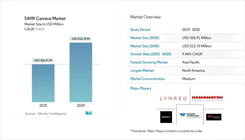
단파장 적외선(SWIR) 카메라 시장 규모는 2025년에 3억 2,691만 달러로 평가되었고, 2030년까지 5억 1,370만 달러로 확대되며 예측 기간 중 CAGR은 9.46%를 나타낼 전망입니다.
본 보고서는 스캔 방식(에리어 스캔, 라인 스캔), 검출기 기술(InGaAs, MCT, CQD, II형 초격자), 용도(산업용 검사, 감시·보안, 기타),스펙트럼 대역(0.9-1.4 Aµm, 1.4-2.2 Aµm, 기타), 플랫폼(고정형/설치형 시스템, 기타), 지역별로 분류되어 있습니다. 시장 예측은 금액(달러) 기준으로 제시되어 있습니다.
세계의 단파장 적외선(SWIR) 카메라 시장 동향 및 인사이트
반도체 웨이퍼 검사 분야에서의 채택 증가
2025년까지 주요 반도체 제조 공장에서는 가시광선 이미지로는 감지할 수 없었던 표면 아래의 결함을 파악하기 위해 단파장 적외선(SWIR) 카메라가 활용되기 시작했습니다. 300mm 및 450mm 웨이퍼로의 지속적인 전환에 따라 수율 확보의 중요성이 높아지면서, 양산 과정에서 단파장 적외선 검사는 필수적인 요소가 되었습니다. New Imaging Technologies사의 NSC1801 센서는 고처리량 노광 라인을 지원하는 60kHz의 라인 속도를 실현하고, 픽셀 아키텍처의 소형화를 통해 검사 대상 1개 사이트당 비용을 절감했습니다. 메가팹으로의 집약이 진행됨에 따라 품질 기준이 엄격해졌으며, 단파장 적외선(SWIR) 카메라는 단순한 옵션 추가 기능에서 공정 내 표준 도구로 그 위상이 높아졌습니다. 벤더들의 표준화 노력으로 통합이 더욱 원활해졌으며, 투자 회수 기간이 단축되었습니다.
방위용 야간 투시 시스템 업그레이드
NATO 회원국이 자금을 지원한 현대화 프로그램에서는 기존의 고글과 소총 조준경에 열화상 및 단파장 적외선(SWIR) 이미지를 융합한 듀얼 밴드 모듈이 후속 장착되었습니다. LRAS3 등의 프로그램에서는 안개나 전장의 연기에 가려져 있던 표적이 SWIR 채널을 통해 재식별될 때 얻을 수 있는 전술적 우위가 입증되었습니다. Sensor Unlimited사의 Hinted SWIR 기술은 눈에 무해한 레이저 조명을 활용하여, 열화상 시스템에는 부족했던 ‘비밀 작전 유지’라는 특성을 갖추고 있었습니다. 수출 규제에 따른 시장 세분화는 국내 수요를 보호하는 동시에, 동맹국에 대한 보다 광범위한 보급을 위한 ITAR 적용 대상에서 제외된 변형 제품 개발을 촉진했습니다. 2030년까지 이어지는 조달 로드맵은 공급업체에게 장기적인 수익 전망이 확보되어 있음을 뒷받침합니다.
이중용도 적외선 기술에 대한 수출 규제
카테고리 XII 개정안에 따라 더 많은 초점면 어레이가 ITAR 적용 대상이 되었으며, 비동맹국으로의 고해상도 SWIR 모듈 출하가 제한되었습니다. 규정 준수를 위한 조치로 인해 라이선싱 지연 및 법적 비용이 발생하여 소규모 수출업체들에게 걸림돌이 되었습니다. Xenics와 같은 공급업체들은 ITAR 적용 대상이 아닌 카메라 제품 라인을 출시하여 대응했으나, 성능 측면에서의 타협은 여전히 남아 있었습니다. 이러한 규제의 불일치로 인해 프렌드쇼어링의 지위와 보다 원활한 수출 승인을 추구하며, 유럽 파운드리로의 생산 이전이 진행되었습니다. 시간이 지남에 따라 이러한 추가적인 마찰로 인해 전 세계 연평균 성장률(CAGR)은 소폭 둔화되었지만, 동시에 개방형 수출 아키텍처에서의 혁신을 촉진하는 결과로 이어지기도 했습니다.
부문별 분석
라인 스캔 아키텍처는 컨베이어나 웹의 형태가 주요 요소가 되는 제한적이긴 하지만 점차 확대되고 있는 이용 사례에 대응했습니다. 에리어 스캔 카메라는 범용성이 높은 풀 프레임 촬영을 실현하여 2024년에는 매출의 71.87%를 차지했지만, 단파장 적외선(SWIR) 카메라 시장에서는 2030년까지 라인 스캔 방식이 연평균 성장률(CAGR) 10.78%로 유지될 것으로 전망됩니다. New Imaging Technologies사의 Lisa SWIR 플랫폼은 이러한 동향을 여실히 보여주며, 2,048픽셀 어레이와 60kHz의 라인 레이트를 결합하여 반도체 및 재활용용 컨베이어와 원활하게 동기화되었습니다. 결함 본딩 기술의 향상으로 데드 픽셀이 감소함에 따라, 에어리어 스캔에 필적하는 생산 수율을 달성했습니다. 제조업체들은 광학적 제약이 아닌 공정 흐름에 기반하여 스캔 아키텍처를 선택하는 경향이 강해졌으며, 이러한 변화로 인해 조달 기준의 폭이 넓어졌습니다.
에리어 스캔 모델은 모니터링, 연구 개발(R&D), 과학 이미징 분야에서 여전히 필수적이며, 이러한 분야에서는 원시 데이터 처리 능력보다 장면 전체의 맥락이 더 중요하게 여겨졌습니다. 각 공급업체는 픽셀 크기와 냉각 옵션을 다양화하여 신흥 라인 스캔 제품과 동등한 성능을 확보했습니다. 스캔 방식 간의 상호 작용은 건전한 경쟁을 촉진하여 감도와 다이나믹 레인지의 전반적인 향상을 가져왔습니다.
InGaAs는 수십 년에 걸친 방위 분야에서의 실적과 성숙한 공급망을 바탕으로, 2024년 단파장 적외선(SWIR) 카메라 시장에서 82.76%의 점유율을 유지하며 여전히 주류 위치를 차지했습니다. 그럼에도 불구하고 ST마이크로일렉트로닉스 등 제조업체들이 1.62µm의 픽셀 피치에서 양자 효율 60%의 장치를 소비자용 가격대로 출시함에 따라, 콜로이드 양자점 센서는 연평균 성장률(CAGR) 11.34%를 나타낼 것으로 전망되었습니다. 양자점이 300mm 실리콘 팹과 호환되게 됨에 따라 비용 구조가 획기적으로 개선되었고, 이 기술은 스마트폰의 얼굴 인식, 자동차 실내 모니터링, 그리고 신흥 AR 웨어러블 기기로의 확대 적용이 가능해졌습니다. 유형 II 초격자 검출기는 밴드갭 공학을 활용하여 스펙트럼 범위를 3µm 이상으로 확장함으로써 틈새 과학 분야 및 우주용 페이로드 시장을 확보했습니다.
비용 측면에서의 우위는 양자점에 유리하게 작용했지만, 채택의 진전은 장기 안정성, 암전류 성능 및 내방사선성 벤치마크에 좌우되었습니다. 주요 OEM 기업들은 검증된 InGaAs의 신뢰성과 나노 소재 진출기업들의 획기적인 가격 책정 사이에서 균형을 맞추기 위해 듀얼 소싱 전략을 시작했습니다.
지역별 분석
북미는 국방 예산, 반도체 생산 능력, 그리고 정밀 농업 분야의 조기 도입에 힘입어 2024년 매출의 37.15%를 차지했습니다. 온세미(Onsemi)의 SWIR Vision Systems 인수와 하마마츠 포토닉스(Hamamatsu Photonics)의 BAE Systems Imaging Solutions 인수로 인해 중요한 검출기 지적 재산권(IP)이 이 지역 내의 관리 하에 통합되었습니다. 수출 규제는 국내 기업을 특정 해외 경쟁사로부터 보호하는 동시에, ITAR(국제무기거래규정)의 적용을 받지 않는 대체 기술의 연구 개발을 촉진했습니다. 이 지역의 성숙한 OEM 생태계는 인플레이션 압력에도 불구하고 갱신 주기를 유지했습니다.
아시아태평양은 중국의 반도체 투자, 한국의 메모리 공장, 그리고 인도 및 동남아시아 전역의 농업 기술 시범 사업에 힘입어 11.28%라는 가장 빠른 연평균 성장률(CAGR)을 기록했습니다. 지방 자치 단체는 이미징 부품의 자급자족을 추진하며, 양자점 및 게르마늄 검출기를 다루는 스타트업 기업에 보조금을 지원했습니다. 일본의 정밀 기기 제조업체는 광학 분야에서 오랫동안 쌓아온 리더십을 활용하여 SWIR 모듈을 계측 기기에 통합했습니다.
유럽에서는 순환형 경제 지침 및 기후 변화 적응에 관한 규제적 시급성이 높아지는 가운데 시장이 확대되었습니다. Lynred사가 8,500만 유로를 투자하여 그르노블에서 진행한 확장 사업은 2025년까지 해당 지역의 검출기 생산 능력을 50% 끌어올리고, 유럽우주국(ESA) 및 방위 프로그램에 대한 공급을 확보하는 것을 목표로 했습니다. 국경을 초월한 프로젝트를 통해 플라스틱 분리 수거 인프라 기준이 통일되었으며, 거시경제의 역풍에도 불구하고 안정적인 수요가 유지되었습니다.
기타 혜택 :
- 엑셀 형식 시장 예측(ME) 시트
- 3개월간 애널리스트 지원
자주 묻는 질문
목차
제1장 서론
제2장 조사 방법
제3장 개요
제4장 시장 구도
제5장 시장 규모 및 성장 예측
제6장 경쟁 구도
제7장 시장 기회 및 향후 전망
KTH 26.09.02According to Mordor Intelligence, the shortwave infrared (SWIR) camera market size reached USD 326.91 million in 2025 and is projected to expand to USD 513.70 million by 2030, representing a 9.46% CAGR over the forecast period.
This report is Segmented by Scanning Type (Area Scan, and Line Scan), Detector Technology (InGaAs, MCT, CQD, and Type-II Superlattice), Application (Industrial Inspection, Surveillance and Security, and More), Spectral Band (0. 9 - 1. 4 Aµm, 1. 4 - 2. 2 Aµm, and More), Platform (Fixed/Mounted Systems, and More), and Geography. The Market Forecasts are Provided in Terms of Value (USD).
Global SWIR Camera Market Trends and Insights
Rising adoption in semiconductor wafer inspection
By 2025, leading fabs relied on SWIR cameras to pinpoint subsurface defects once masked in visible imagery. Continuous transitions to 300 mm and 450 mm wafers heightened the stakes for yield protection, making short-wave infrared inspection indispensable for volume production. New Imaging Technologies' NSC1801 sensor delivered 60 kHz line rates that aligned with high-throughput lithography lines, while smaller pixel architectures reduced cost per site tested. Consolidation around mega-fabs intensified quality metrics, elevating SWIR cameras from optional add-ons to baseline process tools. Standardization efforts by equipment vendors further smoothed integration and shortened payback cycles.
Defense night-vision system upgrades
Modernization programs funded by NATO allies retrofitted legacy goggles and riflescopes with dual-band modules marrying thermal and SWIR imagery. Programs such as LRAS3 demonstrated the tactical edge obtained when targets hidden in fog or battlefield smoke reappeared in the SWIR channel. Sensor Unlimited's Hinted SWIR technology leveraged eye-safe laser illumination to preserve covert operations, an attribute thermal systems lacked. Export-control segmentation created sheltered domestic demand while encouraging ITAR-free variants for broader allied distribution. Procurement roadmaps running through 2030 underscored the long-tail revenue visibility for suppliers.
Export controls on dual-use infrared technology
Proposed updates to Category XII placed additional focal-plane arrays under ITAR, limiting shipment of high-resolution SWIR modules to non-allied territories. Compliance added licensing delays and legal costs that hampered small exporters. Suppliers such as Xenics responded by launching ITAR-free camera lines, though performance tradeoffs persisted. The regulatory patchwork encouraged production moves to European foundries, seeking friend-shored status and smoother export approval. Over time, the extra friction modestly dampened global CAGR yet simultaneously drove innovation in open-export architectures.
Other drivers and restraints analyzed in the detailed report include:
- Regulations mandating NIR sorting for plastic recycling
- Growth of hyperspectral crop-health imaging
- High InGaAs wafer fabrication costs
For complete list of drivers and restraints, kindly check the Table Of Contents.
Segment Analysis
Line-scan architectures served narrow but expanding use cases where conveyor or web geometry dominated. Although area-scan cameras delivered versatile full-frame capture and retained 71.87% revenue in 2024, the shortwave infrared (SWIR) camera market registered a 10.78% CAGR for line-scan through 2030. New Imaging Technologies' Lisa SWIR platform underscored the trend, pairing 2,048-pixel arrays with 60 kHz line rates that synced seamlessly with semiconductor and recycling conveyors. Improvements in defect-bonding reduced dead pixels, establishing production yields rivaling area-scan economics. Manufacturers increasingly selected scanning architecture based on process flow rather than optical limitation, a shift that broadened procurement criteria.
Area-scan models remained vital across surveillance, R&D, and scientific imaging, where full-scene context outweighed raw throughput. Suppliers diversified pixel sizes and cooling options, ensuring performance parity with emerging line-scan offerings. The interplay between scanning types fostered healthy competition that drove universal gains in sensitivity and dynamic range.
InGaAs remained the incumbent with 82.76% shortwave infrared (SWIR) camera market share in 2024, supported by decades of defense heritage and mature supply chains. Nonetheless, colloidal-quantum-dot sensors delivered an 11.34% CAGR outlook as manufacturers such as STMicroelectronics unveiled 60% quantum efficiency devices at 1.62 µm pixel pitches priced for consumer tiers. Quantum-dot compatibility with 300 mm silicon fabs collapsed cost structures, positioning the technology for smartphone face recognition, automotive cabin monitoring, and emerging AR wearables. Type-II superlattice detectors captured niche scientific and space payloads, leveraging band-gap engineering to extend spectral reach past 3 µm.
While cost advantages weighed in favor of quantum dots, adoption curves hinged on long-term stability, dark current performance, and radiation hardness benchmarks. Tier-one OEMs initiated dual-sourcing strategies that balanced proven InGaAs reliability against disruptive pricing from nanomaterial entrants.
Complete Report Scope:
- By Scanning Type
- Area Scan
- Line Scan
- By Detector Technology
- Indium Gallium Arsenide (InGaAs)
- Mercury Cadmium Telluride (MCT)
- Colloidal Quantum Dot (CQD) and Type-II Superlattice
- By Application
- Industrial Inspection
- Surveillance and Security
- Scientific Research
- Medical and Life-Sciences
- Agricultural Monitoring
- Other Application
- By Spectral Band
- 0.9 - 1.4 Aµm
- 1.4 - 2.2 Aµm
- 2.2 - 3.0 Aµm
- By Platform / Form Factor
- Fixed / Mounted Systems
- Handheld and Portable Cameras
- UAV / Drone-Integrated Payloads
- By Geography
- North America
- United States
- Canada
- Mexico
- South America
- Brazil
- Rest of South America
- Europe
- Germany
- United Kingdom
- France
- Russia
- Rest of Europe
- Asia Pacific
- China
- India
- Japan
- South Korea
- Rest of Asia Pacific
- Middle East and Africa
- Middle East
- Saudi Arabia
- Israel
- Turkey
- Rest of Middle East
- Africa
- South Africa
- Rest of Africa
- Middle East
- North America
Geography Analysis
North America held 37.15% of 2024 revenue, anchored by defense budgets, semiconductor capacity, and early adoption in precision agriculture. Onsemi's acquisition of SWIR Vision Systems and Hamamatsu's purchase of BAE Systems Imaging Solutions consolidated critical detector IP under regional control. Export regulations sheltered domestic players from certain overseas competitors while fueling R&D into ITAR-free alternatives. The region's mature OEM ecosystem sustained replacement cycles despite inflationary pressure.
Asia-Pacific recorded the fastest 11.28% CAGR, catalyzed by semiconductor investment in China, memory fabs in South Korea, and agricultural-tech pilots across India and Southeast Asia. Local governments promoted self-reliance in imaging components, channeling subsidies toward quantum-dot and germanium detector startups. Japanese precision equipment makers integrated SWIR modules into metrology tools, leveraging historic optics leadership.
Europe advanced on regulatory urgency around circular-economy directives and climate adaptation. Lynred's EUR 85 million Grenoble expansion aimed to raise regional detector capacity 50% by 2025, safeguarding supply for ESA and defense programs. Cross-border projects harmonized standards for plastic-sorting infrastructure, supporting stable demand irrespective of macroeconomic headwinds.
- Teledyne Technologies Incorporated
- Hamamatsu Photonics K.K.
- Sony Corporation
- Lynred
- Allied Vision Technologies GmbH
- FLIR Systems LLC (Teledyne FLIR)
- Xenics NV
- Raptor Photonics Ltd.
- New Imaging Technologies SAS
- Princeton Infrared Technologies Inc.
- Sensors Unlimited Inc. (RTX)
- IRCameras LLC
- SCD USA Infrared LLC
- InfiRay Technologies Co. Ltd.
- FluxData Inc.
- SWIR Vision Systems Inc.
- Photon etc. Inc.
- Opgal Optronic Industries Ltd.
- TriEye Technologies Ltd.
Additional Benefits:
- The market estimate (ME) sheet in Excel format
- 3 months of analyst support
TABLE OF CONTENTS
1 INTRODUCTION
- 1.1 Study Assumptions and Market Definition
- 1.2 Scope of the Study
2 RESEARCH METHODOLOGY
3 EXECUTIVE SUMMARY
4 MARKET LANDSCAPE
- 4.1 Market Overview
- 4.2 Market Drivers
- 4.2.1 Rising Adoption In Semiconductor Wafer Inspection
- 4.2.2 Defense Night-Vision System Upgrades
- 4.2.3 Regulations Mandating NIR Sorting for Plastic Recycling
- 4.2.4 Growth of Hyperspectral Crop-Health Imaging
- 4.2.5 Maturation of Colloidal-Quantum-Dot (CQD) SWIR Sensors
- 4.2.6 Edge-AI Integration Lowering Processing Latency
- 4.3 Market Restraints
- 4.3.1 Export Controls on Dual-Use Infrared Technology
- 4.3.2 High Ingaas Wafer Fabrication Costs
- 4.3.3 Thermal-Noise Management Limits on UAV Payloads
- 4.3.4 Competitive Encroachment from Extended-Visible and Lidar Systems
- 4.4 Industry Value Chain Analysis
- 4.5 Regulatory Landscape
- 4.6 Technological Outlook
- 4.7 Porter's Five Forces Analysis
- 4.7.1 Threat of New Entrants
- 4.7.2 Bargaining Power of Suppliers
- 4.7.3 Bargaining Power of Buyers
- 4.7.4 Threat of Substitutes
- 4.7.5 Industry Rivalry
5 MARKET SIZE AND GROWTH FORECASTS (VALUE)
- 5.1 By Scanning Type
- 5.1.1 Area Scan
- 5.1.2 Line Scan
- 5.2 By Detector Technology
- 5.2.1 Indium Gallium Arsenide (InGaAs)
- 5.2.2 Mercury Cadmium Telluride (MCT)
- 5.2.3 Colloidal Quantum Dot (CQD) and Type-II Superlattice
- 5.3 By Application
- 5.3.1 Industrial Inspection
- 5.3.2 Surveillance and Security
- 5.3.3 Scientific Research
- 5.3.4 Medical and Life-Sciences
- 5.3.5 Agricultural Monitoring
- 5.3.6 Other Application
- 5.4 By Spectral Band
- 5.4.1 0.9 - 1.4 Aµm
- 5.4.2 1.4 - 2.2 Aµm
- 5.4.3 2.2 - 3.0 Aµm
- 5.5 By Platform / Form Factor
- 5.5.1 Fixed / Mounted Systems
- 5.5.2 Handheld and Portable Cameras
- 5.5.3 UAV / Drone-Integrated Payloads
- 5.6 By Geography
- 5.6.1 North America
- 5.6.1.1 United States
- 5.6.1.2 Canada
- 5.6.1.3 Mexico
- 5.6.2 South America
- 5.6.2.1 Brazil
- 5.6.2.2 Rest of South America
- 5.6.3 Europe
- 5.6.3.1 Germany
- 5.6.3.2 United Kingdom
- 5.6.3.3 France
- 5.6.3.4 Russia
- 5.6.3.5 Rest of Europe
- 5.6.4 Asia Pacific
- 5.6.4.1 China
- 5.6.4.2 India
- 5.6.4.3 Japan
- 5.6.4.4 South Korea
- 5.6.4.5 Rest of Asia Pacific
- 5.6.5 Middle East and Africa
- 5.6.5.1 Middle East
- 5.6.5.1.1 Saudi Arabia
- 5.6.5.1.2 Israel
- 5.6.5.1.3 Turkey
- 5.6.5.1.4 Rest of Middle East
- 5.6.5.2 Africa
- 5.6.5.2.1 South Africa
- 5.6.5.2.2 Rest of Africa
- 5.6.5.1 Middle East
- 5.6.1 North America
6 COMPETITIVE LANDSCAPE
- 6.1 Market Concentration
- 6.2 Strategic Moves
- 6.3 Market Share Analysis
- 6.4 Company Profiles (includes Global level Overview, Market level overview, Core Segments, Financials as available, Strategic Information, Market Rank/Share for key companies, Products and Services, and Recent Developments)
- 6.4.1 Teledyne Technologies Incorporated
- 6.4.2 Hamamatsu Photonics K.K.
- 6.4.3 Sony Corporation
- 6.4.4 Lynred
- 6.4.5 Allied Vision Technologies GmbH
- 6.4.6 FLIR Systems LLC (Teledyne FLIR)
- 6.4.7 Xenics NV
- 6.4.8 Raptor Photonics Ltd.
- 6.4.9 New Imaging Technologies SAS
- 6.4.10 Princeton Infrared Technologies Inc.
- 6.4.11 Sensors Unlimited Inc. (RTX)
- 6.4.12 IRCameras LLC
- 6.4.13 SCD USA Infrared LLC
- 6.4.14 InfiRay Technologies Co. Ltd.
- 6.4.15 FluxData Inc.
- 6.4.16 SWIR Vision Systems Inc.
- 6.4.17 Photon etc. Inc.
- 6.4.18 Opgal Optronic Industries Ltd.
- 6.4.19 TriEye Technologies Ltd.
7 MARKET OPPORTUNITIES AND FUTURE OUTLOOK
- 7.1 White-Space and Unmet-Need Assessment