

|
시장보고서
상품코드
2122312
반도체 웨이퍼 그라인딩 및 폴리싱 장비 : 시장 점유율 분석, 업계 동향과 통계, 성장 예측(2026-2031년)Semiconductor Wafer Polishing And Grinding Equipment - Market Share Analysis, Industry Trends & Statistics, Growth Forecasts (2026 - 2031) |
||||||
 Mordor Intelligence
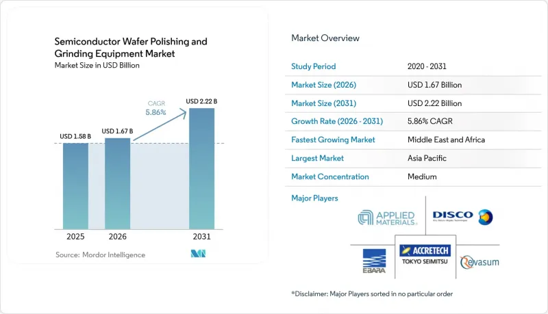
Mordor Intelligence에 의하면, 반도체 웨이퍼 그라인딩 및 폴리싱 장비 시장 규모는 2025년 15억 8,000만 달러에서 2026년에는 16억 7,000만 달러에 이르고, 2026-2031년 CAGR 5.86%로 성장을 지속하여 2031년에는 22억 2,000만 달러에 달할 것으로 예측됩니다.
(1) 반도체산업협회(SIA), “2024년 미국 반도체 산업의 현황”. 본 보고서는 장비 유형별(웨이퍼 연삭 장비, 기타), 웨이퍼 크기별(150mm 이하, 200mm, 300mm, 450mm 이상),기술별(백 그라인딩, 기타), 반도체 유형별(메모리, 로직·SoC, 기타), 최종 사용자별(수직 통합형 디바이스 제조업체, 기타), 지역(북미, 남미, 유럽, 아시아태평양, 중동 및 아프리카)별로 분류되어 있습니다.
전 세계 반도체 웨이퍼 그라인딩 및 폴리싱 장비 시장 동향 및 인사이트
아시아에서 첨단 노드 칩을 탑재한 가전제품의 소비 확대
중국, 인도, 동남아시아 전역에서 플래그십 스마트폰 및 AI 탑재 웨어러블 기기의 급속한 보급으로 인해, 원자 수준에서 매끄러운 웨이퍼 표면과 10억 분의 1 단위로 측정되는 결함 밀도가 필요한 3nm 이하 디바이스에 대한 수요가 가속화되었습니다. 현지 파운드리 기업들은 수출 허가 불확실성에도 불구하고 CMP 및 미세 연삭 생산 능력을 확대한 반면, 장비 제조업체들은 평탄성을 해치지 않으면서도 엄격한 환경 기준을 충족하는 무염소 패드를 도입했습니다. 멀티코어 SoC의 보급에 따라 다양한 재료 스택 전반에 걸친 공정의 균일성이 극히 중요해졌으며, 이종 층에 특화된 적응형 제어 CMP 시스템에 대한 투자가 촉진되었습니다.
미세화 진전에 따른 300mm·450mm CMP 장비 수요 증가
비용 효율이 뛰어난 다이 밀도를 추구함에 따라 300mm는 계속해서 주류 형태로 자리 잡았으나, 더 큰 블랭크를 사용함으로써 다이 면적이 2.25배가 되기 때문에 450mm에 대한 시험적인 개발이 다시 주목을 받았습니다. 각 장비 제조업체들은 플래튼을 강화하고, 슬러리 분포를 최적화하며, 현장 측정 기능을 탑재함으로써 더 넓은 표면에 걸쳐 nm 수준의 제거 균일성을 유지하고, 스케일업이라는 과제에 대응해 왔습니다. TSMC가 시제품으로 제작한 510mm×515mm의 직사각형 기판은 기존 장비 아키텍처를 전면적으로 개편하지 않고도 사용 가능 면적을 3배로 확대할 수 있는 대안을 제시한 것이었습니다.
300mm용 장비의 높은 설비 투자 비용과 긴 투자 회수 기간
2024년 기준에서 300mm CMP 플랫폼 1대의 가격은 300만-500만 달러에 달하며, 설비 업그레이드에는 추가로 100만-200만 달러가 더 필요하기 때문에 생산량이 적은 팹에서는 투자 회수 기간이 4년 이상 소요되었습니다. 중소규모 제조업체들은 확장을 연기하고 재생품이나 공유 용량 모델을 선택했기 때문에 규모 확장에 따른 웨이퍼당 비용 측면에서 분명한 이점이 있음에도 불구하고 장비 도입 속도는 전반적으로 둔화되었습니다.
부문 분석
CMP 장비는 2025년 매출의 55.92%를 차지하며, 0.1nm 이하의 제거 정밀도가 요구되는 첨단 노드의 평탄도 목표 달성에 있어 여전히 중심적인 역할을 수행했습니다. 반도체 웨이퍼 그라인딩 및 폴리싱 장비 시장은 팹이 3nm 이하의 수율 향상을 도모하기 위해 연마제가 포함되지 않은 슬러리와 AI를 활용한 엔드포인트 감지를 채택함으로써 혜택을 받았습니다. 연삭·연마 일체형 플랫폼은 웨이퍼 이송 횟수를 줄이고, 입자 위험을 감소시키며, 대기 시간을 단축했습니다.
고객들이 공정을 통합하여 클린룸 공간을 확보함에 따라, 통합 시스템의 2031년 CAGR은 7.55%로, 독립형 그라인더를 상회했습니다. 각 벤더는 폐쇄 루프 온도 제어, 예측 유지보수, 소모품 수명 분석을 통합하여 다품종 생산에서 OEE(종합 설비 가동률)를 향상시켰습니다. 새롭게 등장한 래핑 및 슬라이싱 장비는 다이아몬드 및 기타 초경질 기판을 지원하여, 반도체 웨이퍼 그라인딩 및 폴리싱 장비 시장의 범위를 틈새 시장인 포토닉스 및 양자 소자 부문까지 확대했습니다.
2025년 시장 매출 중 300mm 노드가 61.88%를 차지할 것으로 예상되며, 이는 수십 년에 걸친 공정의 성숙, 소모품의 최적화, 충분히 감가상각이 진행된 팹 자산이 뒷받침하고 있습니다. CMP 패드의 텍스처와 백그라인드 휠 형태에 대한 지속적인 개선으로 처리량이 더욱 향상되어, 반도체 웨이퍼 그라인딩 및 폴리싱 장비 시장에서 이 부문의 경제적 우위가 강화되었습니다.
한편, 450mm 이상 카테고리는 웨이퍼 1장당 다이 수를 3배로 늘릴 것으로 기대되는 직사각형 형태를 모색하는 파일럿 라인에 힘입어 10.84%라는 가장 높은 연평균 성장률(CAGR)을 기록했습니다. 각 장비 제조업체들은 여러 직경에 대응 가능한 대형 플래튼, 로봇 핸들러, 대용량 슬러리 공급 시스템의 프로토타입을 개발하고 있으며, 반도체 웨이퍼 그라인딩 및 폴리싱 장비 산업이 대규모 ROI 평가를 진행하는 가운데, 2028년 이후의 대량 도입에 대비해 체제를 정비하고 있습니다.
지역별 분석
2025년, 아시아태평양은 전 세계 매출의 67.94%를 계속 차지했습니다. 이는 대만, 한국, 일본, 중국이 주도한 결과로, 이들 지역에서는 집적 소자의 로드맵과 파운드리 확장에 따라 장비 조달이 지속되었습니다. TSMC의 염소 프리 패드 도입과 일본의 보조금 지원을 받은 팹 클러스터 형성은 이 지역의 친환경 장비에 대한 선호도를 높였습니다. 수출 규제의 불확실성으로 인해 중국의 팹은 현지 공급업체에 대한 의존도를 높였지만, 라이선스 예외 조치를 통해 하이엔드 CMP 수입은 지속되어 반도체 웨이퍼 그라인딩 및 폴리싱 장비 시장의 기초적인 수요는 유지되었습니다.
북미에서는 2022년 ‘CHIPS and Science Act’를 계기로 투자가 회복되는 모습을 보였습니다. 이 법안은 520억 달러 규모의 인센티브를 동원하여, 2025년까지 총액 4,500억 달러에 육박하는 90건 이상의 팹 건설 계획 발표를 촉진했습니다. 생산 능력 확대로 인해 장비 수주는 증가했으나, 2030년까지 6만 7,000명 규모의 기술자 부족이 예상에 따라 자동화의 우선순위가 높아졌고, 인재 공급을 가속화하기 위해 학술 컨소시엄과의 제휴가 추진되었습니다.
이에 이어 유럽에서는 2030년까지 세계 생산 점유율 20%를 목표로 하는 430억 유로(498억 3,000만 달러) 규모의 ‘칩스법(CHIPS Act)’이 제정되었습니다. 독일의 정밀 공학 기업, 프랑스의 첨단 패키징 거점, 북유럽의 재료 과학 연구소는 에너지 회수 펌프와 물 재활용 루프를 갖춘 CMP 시스템을 요구하며, 조달을 EU 그린딜의 목표와 연계하는 동시에 반도체 웨이퍼 그라인딩 및 폴리싱 장비 시장에서 차별화된 솔루션의 육성을 촉진했습니다.
기타 혜택
- 엑셀 형식 시장 예측(ME) 시트
- 3개월간의 애널리스트 지원
자주 묻는 질문
목차
제1장 서론
제2장 조사 방법
제3장 주요 요약
제4장 시장 구도
제5장 시장 규모와 성장 예측
제6장 경쟁 구도
제7장 시장 기회와 향후 전망
LSH 26.09.04According to Mordor Intelligence, the semiconductor wafer polishing and grinding equipment market size is expected to grow from USD 1.58 billion in 2025 to USD 1.67 billion in 2026 and is forecast to reach USD 2.22 billion by 2031 at 5.86% CAGR over 2026-2031.
[1] Semiconductor Industry Association, "2024 State of the U.S. This report is Segmented by Equipment Type (Wafer Grinding Machines, and More), Wafer Size (<=150 Mm, 200 Mm, 300 Mm, and 450 Mm and Above), Technology (Back-Grinding, and More), Semiconductor Type (Memory, Logic and SoC, and More), End-User (Integrated Device Manufacturers, and More), and Geography (North America, South America, Europe, Asia-Pacific, and Middle East and Africa).
Global Semiconductor Wafer Polishing And Grinding Equipment Market Trends and Insights
Growing consumption of consumer electronics with advanced-node chips in Asia
Rapid uptake of flagship smartphones and AI-enabled wearables across China, India, and Southeast Asia accelerated demand for sub-3 nm devices that require atomically smooth wafer surfaces and defect densities measured in parts per billion. Local foundries expanded CMP and fine-grinding capacity despite export-license uncertainty, while tool makers introduced chlorine-free pads that met strict environmental codes without compromising planarity. As multi-core SoCs proliferated, process uniformity across diverse material stacks became critical, spurring investment in adaptive-control CMP systems tailored for heterogeneous layers.
Miniaturization push driving demand for 300 mm and 450 mm CMP tools
The search for cost-effective die density sustained 300 mm as the mainstream format, yet exploratory 450 mm development resurfaced because a larger blank yields 2.25 times more die area. Tool makers tackled the scale-up challenge by reinforcing platens, optimizing slurry distribution, and embedding in-situ metrology to maintain nanometer-level removal uniformity across wider surfaces. TSMC's prototype 510 mm X 515 mm rectangular substrate hinted at an alternate path that could triple usable area without fully overhauling legacy tool architectures.
High capital cost and long ROI cycle for 300 mm tools
A single 300 mm CMP platform carried a USD 3-5 million price tag in 2024, with facility upgrades adding USD 1-2 million, stretching payback beyond 4 years in lower-volume fabs. Smaller players delayed expansion and opted for refurbished or shared-capacity models, slowing overall tool uptake despite clear cost-per-die advantages at scale.
Other drivers and restraints analyzed in the detailed report include:
- Foundry capacity investments in the U.S. and Europe under the CHIPS Act
- Transition to SiC/GaN power devices requires ultra-precision grinding
- Export controls and IP barriers limiting shipments to China
For complete list of drivers and restraints, kindly check the Table Of Contents.
Segment Analysis
CMP tools generated 55.92% of 2025 revenue and remained central to advanced-node planarity targets that mandate removal accuracy below 0.1 nm. The semiconductor wafer polishing and grinding equipment market benefited as fabs adopted abrasive-free slurries and AI-assisted endpoint detection to push sub-3 nm yields upward. Integrated grinder-polisher platforms reduced wafer transfers, trimming particle risks, and cutting queue time.
Integrated systems' 7.55% CAGR through 2031 outpaced standalone grinders as customers consolidated process steps to free cleanroom space. Vendors bundled closed-loop temperature control, predictive maintenance, and consumable-life analytics, enhancing OEE for high-mix production. Emerging lapping and slicing tools addressed diamond and other ultra-hard substrates, extending the semiconductor wafer polishing and grinding equipment market reach into niche photonics and quantum-device lines.
The 300 mm node held 61.88% of 2025 market revenue, underlining decades of process maturity, optimized consumables, and well-depreciated fab assets. Continuous enhancements in CMP pad texture and back-grinding wheel geometry further raised throughput, reinforcing the segment's economic moat within the semiconductor wafer polishing and grinding equipment market.
Conversely, the 450 mm and above category registered the fastest 10.84% CAGR, driven by pilot lines exploring rectangular formats that promise 3X more die per wafer. Equipment makers prototyped enlarged platens, robotic handlers, and high-capacity slurry-delivery systems adaptable to multiple diameters, positioning themselves for potential mass adoption beyond 2028 as the semiconductor wafer polishing and grinding equipment industry evaluates ROI at scale.
Complete Report Scope:
- By Equipment Type
- Wafer Grinding Machines
- Wafer Polishing (CMP) Equipment
- Integrated Grinder-Polisher Tools
- Others (Lapping, Slicing Thinners)
- By Wafer Size
- <=150 mm
- 200 mm
- 300 mm
- 450 mm and Above
- By Technology
- Back-Grinding
- Double-Side Grinding
- Chemical Mechanical Polishing (CMP)
- Edge-Grinding / Bevel Polishing
- By Semiconductor Type
- Memory (DRAM, NAND)
- Logic and SoC
- Power and Analog (Si, SiC, GaN)
- MEMS and Sensors
- CMOS Image Sensors
- LED and Optoelectronics
- By End-User
- Foundries
- Integrated Device Manufacturers (IDMs)
- OSAT / Advanced Packaging Facilities
- Research and Development Institutes and Pilot Lines
- By Geography
- North America
- United States
- Canada
- South America
- Brazil
- Rest of South America
- Europe
- Germany
- United Kingdom
- France
- Italy
- Rest of Europe
- Asia-Pacific
- China
- Taiwan
- Japan
- South Korea
- India
- Rest of Asia-Pacific
- Middle East and Africa
- Middle East
- Saudi Arabia
- United Arab Emirates
- Turkey
- Rest of Middle East
- Africa
- South Africa
- Nigeria
- Rest of Africa
- Middle East
- North America
Geography Analysis
Asia-Pacific retained 67.94% of global revenue in 2025, anchored by Taiwan, South Korea, Japan, and China, where integrated device roadmaps and foundry expansions sustained tool procurements. TSMC's chlorine-free pad rollout and Japan's subsidy-backed fab clusters reinforced a regional preference for environmentally optimized equipment. Export-control uncertainties nudged Chinese fabs to local suppliers, yet high-end CMP imports persisted via license exceptions, preserving baseline semiconductor wafer polishing and grinding equipment market demand.
North America experienced an investment renaissance following the 2022 CHIPS and Science Act, which mobilized USD 52 billion in incentives and prompted over 90 fab announcements worth nearly USD 450 billion through 2025. Capacity additions raised tool orders, although technician gaps of 67,000 positions by 2030 drove automation priorities and partnerships with academic consortia to accelerate workforce pipelines.
Europe followed with the EUR 43 billion (USD 49.83 billion) Chips Act that targeted a 20% global output share by 2030. Germany's precision-engineering firms, France's advanced-packaging hubs, and Nordic material-science institutes demanded CMP systems featuring energy-recovery pumps and water-recycling loops, aligning procurement with EU Green Deal objectives and fostering differentiated semiconductor wafer polishing and grinding equipment market solutions.
- Applied Materials Inc.
- Ebara Corporation
- DISCO Corporation
- Tokyo Seimitsu Co. Ltd (ACCRETECH)
- Revasum Inc.
- Komatsu NTC Ltd.
- Okamoto Machine Tool Works Co. Ltd.
- Lapmaster Wolters GmbH (Precision Surfacing Solutions)
- Logitech Ltd.
- Entrepix Inc. (Amtech Systems)
- G&N Genauigkeits Maschinenbau Nurnberg GmbH
- Hantop Intelligence Tech Co. Ltd.
- CMP-Tec Inc.
- Koyo Machinery Co. Ltd.
- Shanghai ShinEne Technology Co. Ltd.
- Qingdao Lapping & Polishing Equipment Co. Ltd.
- Nagase Integrex Co. Ltd.
- Strausbaugh Inc. (S-Cubed)
- Pureon AG
- Vibrantz Technologies Inc.
- Axus Technology
- SHANGHAI FAMOUS TRADE CO.,LTD (ZMSH)
- Huahai Machinery Group
- Hansung Engineering Co. Ltd.
- GPMT Co. Ltd.
Additional Benefits:
- The market estimate (ME) sheet in Excel format
- 3 months of analyst support
TABLE OF CONTENTS
1 INTRODUCTION
- 1.1 Study Assumptions and Market Definition
- 1.2 Scope of the Study
2 RESEARCH METHODOLOGY
3 EXECUTIVE SUMMARY
4 MARKET LANDSCAPE
- 4.1 Market Overview
- 4.2 Market Drivers
- 4.2.1 Growing Consumption of Consumer Electronics with Advanced-Node Chips in Asia
- 4.2.2 Miniaturization Push Driving Demand for 300 mm and 450 mm CMP Tools
- 4.2.3 Foundry Capacity Investments in U.S. and Europe under CHIPS Acts
- 4.2.4 Transition to SiC/GaN Power Devices Requiring Ultra-Precision Grinding
- 4.2.5 Yield-Enhancement Needs for 3D-IC and Heterogeneous Integration
- 4.2.6 Sustainability Mandates Advancing Slurry-Free Polishing Technologies
- 4.3 Market Restraints
- 4.3.1 High Capital Cost and Long ROI Cycle for 300 mm Tools
- 4.3.2 Consumables Cost Inflation (Pads, Slurries, Diamond Wheels)
- 4.3.3 Export-Control and IP Barriers Limiting Shipments to China
- 4.3.4 Skilled-Technician Shortage for Process Set-up and Maintenance
- 4.4 Value Chain Analysis
- 4.5 Regulatory or Technological Outlook
- 4.6 Porter's Five Forces
- 4.6.1 Threat of New Entrants
- 4.6.2 Bargaining Power of Buyers
- 4.6.3 Bargaining Power of Suppliers
- 4.6.4 Threat of Substitute Products
- 4.6.5 Intensity of Competitive Rivalry
- 4.7 Industry Value Chain Analysis
- 4.8 Secondary Equipment Market Dynamics
- 4.9 Investment Analysis
- 4.10 Macroeconomic Impact Assessment
5 MARKET SIZE AND GROWTH FORECASTS (VALUE)
- 5.1 By Equipment Type
- 5.1.1 Wafer Grinding Machines
- 5.1.2 Wafer Polishing (CMP) Equipment
- 5.1.3 Integrated Grinder-Polisher Tools
- 5.1.4 Others (Lapping, Slicing Thinners)
- 5.2 By Wafer Size
- 5.2.1 <=150 mm
- 5.2.2 200 mm
- 5.2.3 300 mm
- 5.2.4 450 mm and Above
- 5.3 By Technology
- 5.3.1 Back-Grinding
- 5.3.2 Double-Side Grinding
- 5.3.3 Chemical Mechanical Polishing (CMP)
- 5.3.4 Edge-Grinding / Bevel Polishing
- 5.4 By Semiconductor Type
- 5.4.1 Memory (DRAM, NAND)
- 5.4.2 Logic and SoC
- 5.4.3 Power and Analog (Si, SiC, GaN)
- 5.4.4 MEMS and Sensors
- 5.4.5 CMOS Image Sensors
- 5.4.6 LED and Optoelectronics
- 5.5 By End-User
- 5.5.1 Foundries
- 5.5.2 Integrated Device Manufacturers (IDMs)
- 5.5.3 OSAT / Advanced Packaging Facilities
- 5.5.4 Research and Development Institutes and Pilot Lines
- 5.6 By Geography
- 5.6.1 North America
- 5.6.1.1 United States
- 5.6.1.2 Canada
- 5.6.2 South America
- 5.6.2.1 Brazil
- 5.6.2.2 Rest of South America
- 5.6.3 Europe
- 5.6.3.1 Germany
- 5.6.3.2 United Kingdom
- 5.6.3.3 France
- 5.6.3.4 Italy
- 5.6.3.5 Rest of Europe
- 5.6.4 Asia-Pacific
- 5.6.4.1 China
- 5.6.4.2 Taiwan
- 5.6.4.3 Japan
- 5.6.4.4 South Korea
- 5.6.4.5 India
- 5.6.4.6 Rest of Asia-Pacific
- 5.6.5 Middle East and Africa
- 5.6.5.1 Middle East
- 5.6.5.1.1 Saudi Arabia
- 5.6.5.1.2 United Arab Emirates
- 5.6.5.1.3 Turkey
- 5.6.5.1.4 Rest of Middle East
- 5.6.5.2 Africa
- 5.6.5.2.1 South Africa
- 5.6.5.2.2 Nigeria
- 5.6.5.2.3 Rest of Africa
- 5.6.5.1 Middle East
- 5.6.1 North America
6 COMPETITIVE LANDSCAPE
- 6.1 Market Concentration
- 6.2 Strategic Moves
- 6.3 Market Share Analysis
- 6.4 Company Profiles (includes Global-level Overview, Market-level Overview, Core Segments, Financials, Strategic Information, Market Rank/Share, Products and Services, Recent Developments)
- 6.4.1 Applied Materials Inc.
- 6.4.2 Ebara Corporation
- 6.4.3 DISCO Corporation
- 6.4.4 Tokyo Seimitsu Co. Ltd (ACCRETECH)
- 6.4.5 Revasum Inc.
- 6.4.6 Komatsu NTC Ltd.
- 6.4.7 Okamoto Machine Tool Works Co. Ltd.
- 6.4.8 Lapmaster Wolters GmbH (Precision Surfacing Solutions)
- 6.4.9 Logitech Ltd.
- 6.4.10 Entrepix Inc. (Amtech Systems)
- 6.4.11 G&N Genauigkeits Maschinenbau Nurnberg GmbH
- 6.4.12 Hantop Intelligence Tech Co. Ltd.
- 6.4.13 CMP-Tec Inc.
- 6.4.14 Koyo Machinery Co. Ltd.
- 6.4.15 Shanghai ShinEne Technology Co. Ltd.
- 6.4.16 Qingdao Lapping & Polishing Equipment Co. Ltd.
- 6.4.17 Nagase Integrex Co. Ltd.
- 6.4.18 Strausbaugh Inc. (S-Cubed)
- 6.4.19 Pureon AG
- 6.4.20 Vibrantz Technologies Inc.
- 6.4.21 Axus Technology
- 6.4.22 SHANGHAI FAMOUS TRADE CO.,LTD (ZMSH)
- 6.4.23 Huahai Machinery Group
- 6.4.24 Hansung Engineering Co. Ltd.
- 6.4.25 GPMT Co. Ltd.
7 MARKET OPPORTUNITIES AND FUTURE OUTLOOK
- 7.1 White-space and Unmet-Need Assessment


