

|
시장보고서
상품코드
2122527
박형 웨이퍼 가공 및 다이싱 장비 : 시장 점유율 분석, 업계 동향 및 통계, 성장 예측(2026-2031년)Thin Wafer Processing And Dicing Equipment - Market Share Analysis, Industry Trends & Statistics, Growth Forecasts (2026 - 2031) |
||||||
 Mordor Intelligence
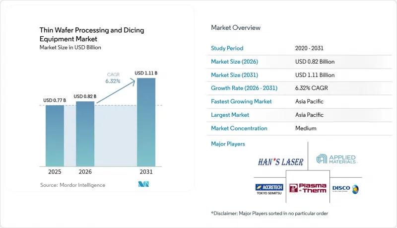
Mordor Intelligence에 의하면, 2026년 박형 웨이퍼 가공 및 다이싱 장비 시장 규모는 8억 2,000만 달러로 추정되고 2025년 7억 7,000만 달러에서 확대해, 2031년에는 11억 1,000만 달러에 이를 것으로 예측됩니다.
2026년부터 2031년까지 연평균 성장률(CAGR) 6.32%로 성장할 것으로 전망됩니다.

본 보고서는 장비 유형(얇게 깎기 장비 및 다이싱 장비), 용도(메모리 및 로직 TSV, MEMS 디바이스, 파워 디바이스 등), 웨이퍼 두께(750mm, 120mm 등),웨이퍼 크기(4인치 미만, 5-6인치 등), 지역(북미, 남미, 유럽, 아시아태평양 등)별로 분류되어 있습니다. 시장 전망은 금액(달러) 기준으로 제시되어 있습니다.
세계의 박형 웨이퍼 가공 및 다이싱 장비 시장 동향 및 인사이트
RFID, 스마트 카드, 자동차용 파워 IC의 채택 확대
비접촉식 결제 카드나 자동차의 전기화에는 고주파 효율과 열 성능을 확보하기 위해 두께가 120µm 이하인 다이가 필요합니다. 배터리식 전기차(BEV)에 탑재되는 실리콘 카바이드(SiC) 트랙션 인버터는 열 저항을 줄이기 위해 두께 100µm 미만의 웨이퍼에 의존하고 있으며, 이것이 고도의 연마,CMP, 그리고 응력 완화 모듈에 대한 수요를 견인하고 있습니다. 자동차 콕핏의 디지털화는 정밀한 두께 제어와 저응력 다이 분리를 필요로 하는 고성능 SoC에 대한 수요를 더욱 부추기고 있습니다. 그 결과, 각 OEM 업체들은 더 좁은 두께 공차와 더 좁은 절단 폭을 지정하고 있으며, 이로 인해 프리미엄 박막화 및 플라즈마 다이싱 장비의 평균 판매 가격이 상승하고 있습니다. 이러한 호재는 박막 웨이퍼 가공 및 다이싱 장비 시장의 매출 확대를 직접적으로 뒷받침하고 있습니다.
3D-IC TSV 메모리 및 로직 수요의 급증
반도체 제조업체들은 평면 스케일링의 한계를 극복하기 위해 수직 통합으로 전환하고 있습니다. TSV 적층형 DRAM이나 칩렛 기반 CPU의 경우 웨이퍼를 50µm 이하로 얇게 가공해야 하지만, 기존의 양면 연마 시스템으로는 뒤틀림을 유발하지 않고 이를 처리할 수 없습니다. 주요 파운드리 기업들은 2nm 로직의 양산 체제 구축을 위해 수십억 달러 규모의 예산을 편성하고 있으며, 여기에는 캐리어 디본드, 레이저 디본드, 플라즈마 다이싱 장비의 대량 도입이 포함됩니다. 이러한 전환으로 인해 처리량 요구 사항은 더욱 높아지고 있습니다. 2nm 팹 한 곳만으로도 월간 6만 장의 300mm 웨이퍼를 소비할 가능성이 있으며, 각 공정에서 TSV의 측벽을 보호하기 위한 초고정밀 싱귤레이션이 필수적입니다. 그 결과, 통합형 계측 기능과 실시간 응력 보정 기능을 갖춘 장비를 제공하는 공급업체들이 얇은 웨이퍼 가공 및 다이싱 장비 시장에서 점유율을 확대되고 있습니다.
웨이퍼의 뒤틀림 및 다이 균열로 인한 수율 저하
웨이퍼 두께를 100µm 미만으로 얇게 하면 내부 응력 구배가 증가하여 연마 후 뒤틀림이 두드러지게 나타납니다. 300mm 기판의 경우, 종종 ±80µm을 초과하기도 합니다. 뒤틀림 보정용 캐리어나 척 레벨의 능동 보정은 비용과 복잡성을 증가시키지만, 여전히 필수적입니다. 왜냐하면 가혹한 TSV 적층 구조에서는 다이 파손으로 인한 수율 손실이 10-15%에 달할 가능성이 있기 때문입니다. 플라즈마를 이용한 싱그레이션에서는 국부적인 발열이 발생하며, 척의 냉각이 불충분할 경우 뒤틀림을 악화시킬 가능성이 있으므로, 폐쇄 루프 방식의 열 관리가 필수적입니다. 결함 밀도 지표가 200µm이라는 기존 기준치에 도달할 때까지는 첨단 박형화 라인의 도입이 단계적으로 이루어질 가능성이 있으며, 이로 인해 박형 웨이퍼 가공 및 다이싱 장비 시장의 단기적인 수익 전망은 둔화될 것으로 예측됩니다.
부문별 분석
2025년, 다이싱 플랫폼은 얇은 웨이퍼 가공 및 다이싱 장비 시장의 63.45% 점유율을 차지하며, 레거시 노드와 최첨단 노드 모두에서 다이싱에 대한 필수적인 수요를 반영했습니다. 기존 블레이드 시스템은 컷당 비용 지표가 성숙기에 접어들었기 때문에 여전히 대량 생산되는 소비자용 IC 시장을 독점하고 있습니다. 그러나 블레이드에 의한 미세 균열을 허용할 수 없는 웨이퍼 레벨 패키지로의 전환이 진행됨에 따라, 플라즈마 방식 및 스텔스 방식 기종의 연간 수주액은 두 자릿수 성장을 기록하고 있습니다. 얇은 웨이퍼 가공 장비는 연평균 성장률(CAGR) 7.06%를 나타낼 것으로 예측되며, 이는 일반 장비의 성장률을 상회하는 수치로, 50µm 미만의 적층 구조로의 아키텍처 전환을 시사합니다. 통합된 계측 기능, 진동이 없는 스테이지, AI 기반 두께 피드백 루프가 결합되어 평균 판매 가격(ASP)을 끌어올리고 있기 때문에 얇은 웨이퍼 가공 및 다이싱 장비 시장에서 얇은 웨이퍼 부문은 이미 단위당 매출 비율 측면에서 우위를 점하고 있습니다.
시장 침투율은 공정 노드의 분화와 병행하여 진행되고 있습니다. 고도의 3D 집적을 목적으로 하는 웨이퍼는 대부분의 경우 두께가 50µm 이하가 될 때까지 백그라인드 공정이 수행된 후, 플라즈마 다이싱이 이루어집니다. 이 공정을 통해 기존 블레이드식 라인에 비해 웨이퍼 1장당 장비 수요가 실질적으로 2배로 증가합니다. 한편, 성숙한 로직 및 아날로그 팹에서는 제품 성능상 초박형 웨이퍼 처리가 필수적이지 않은 한, 설비 투자가 미뤄지고 있습니다. 공급업체들은 모듈식 섀시 설계를 활용하여 기존 라인을 개조함으로써 투자 회수 기간을 단축하고, 초박형 웨이퍼 가공 및 다이싱 장비 시장의 총 접근 가능 시장 규모를 확대되고 있습니다. 이와 동시에, 진공이 필요 없는 플라즈마 챔버를 전문으로 하는 신규 진출기업들이 화합물 반도체 제조업체들을 적극적으로 유치하고 있어, 블레이드 기술에 의존하는 기존 기업들의 점유율을 서서히 빼앗으며 경쟁 환경의 변동을 가속화하고 있습니다.
2025년에는 AI 서버 가속기에 사용되는 HBM 모듈의 3D 적층이 주는 즉각적인 이점으로 인해, 메모리 및 로직용 TSV 공정이 얇은 웨이퍼 가공 및 다이싱 장비 시장 규모의 31.80%를 차지했습니다. 한편, 와이드 밴드갭 디바이스에 의존하는 트랙션 인버터, 차량용 충전기, 재생에너지 관련 전력 변환을 원동력으로 파워 반도체가 8.16%라는 가장 높은 CAGR을 기록하고 있습니다. 이러한 소재는 매우 깨끗한 절단 가장자리가 필요하고 경도도 높기 때문에 플라즈마 및 스텔스 다이싱의 가치 제안과 완벽하게 부합합니다. 전기자동차 출하 대수가 증가함에 따라, 장비에 대한 수요는 웨이퍼 수 증가율을 훨씬 능가하는 속도로 증가하고 있습니다. 이는 SiC 기판이 일반적으로 블레이드 파손을 유발하기 쉬우므로, 조기에 레이저 또는 플라즈마를 이용한 개별 가공으로 전환해야 하기 때문입니다.
파워 부문의 설비 투자 의지에 힘입어, 얇은 웨이퍼 가공 및 다이싱 장비 시장 내 성장 점유율 구도가 재편되고 있습니다. 자동차 OEM의 인증 요건에서는 멀티 사이트에서의 중복성이 요구되고 있어, 이에 따라 장비 도입 대수가 증가하고 있습니다. 한편, MEMS 및 RFID는 계속해서 한 자릿수 중반대의 성장세를 이어가고 있어, 소모품 주도형 블레이드 시스템에 안정적이고 정기적인 부품 매출을 가져다주고 있습니다. CMOS 이미지 센서는 멀티 카메라가 탑재된 스마트폰이나 자율주행용 ADAS 시스템에서 호황을 보이고 있지만, 많은 CIS 팹이 200mm 라인으로 전환되고 있어 300mm TSV 로직에 비해 단가는 억제되고 있습니다. 통합된 제어 소프트웨어를 통해 이러한 다양한 요구 사항에 대응할 수 있는 공급업체는 고객 유지율을 높이고, 고객 1인당 평생 수익을 확보할 수 있습니다.
지역별 분석
2025년에 아시아태평양이 59.65%의 점유율을 차지한 배경에는 대만의 파운드리 업계에서의 주도적 지위, 한국의 메모리 생산량, 그리고 중국의 보조금에 힘입은 생산 능력 확대가 있습니다. 이 지역의 연평균 성장률(CAGR) 8.05%는 2026년까지 가동을 시작할 예정인 4개의 2nm 제조 시설을 포함해 잇달아 발표된 팹 건설 소식의 혜택을 받고 있습니다. 이것만으로도월6만 장의 300mm 웨이퍼와 집중적인 얇은 웨이퍼 가공이 필요합니다. 디스코(DISCO)나 도쿄정밀(Tokyo Seimitsu)과 같은 일본 장비 제조업체들이 블레이드 및 스텔스 다이싱 시스템의 대부분을 공급하고 있으며, 지역 내 공급업체와의 근접성과 충실한 사후 서비스가 얇은 웨이퍼 가공 및 다이싱 장비 시장에서 아시아태평양의 우위를 더욱 공고히 하고 있습니다.
북미는 미국의 산업 정책이 국내 생산을 촉진하고 있어 2위를 차지하고 있습니다. ‘CHIPS 법’의 인센티브에 연동된 파운드리 확장을 위해서는 첨단 CMP, 캐리어 본딩, 플라즈마 다이싱 기술 수입을 포함하여 아시아의 공정 성능과 동등한 수준이 요구되고 있습니다. 다국적 IDM 기업들의 대규모 설비 투자는 장비 공급업체의 투자 회수 기간을 단축시키고, 지역별 수익원을 다각화하고 있습니다. 환경·건강·안전 관련 규제로 인해 팹에서는 블레이드 시스템을 대신해 미세 입자 배출량이 적은 플라즈마 장비의 도입이 진행되고 있으며, 이는 북미의 얇은 웨이퍼 가공 및 다이싱 장비 시장의 기술 구성을 소폭 변화시키고 있습니다.
유럽의 반도체 전략은 자동차용 및 산업용 디바이스에 중점을 두고 있습니다. 투자 대상은 유럽 칩스 법에 힘입은 실리콘 카바이드(SiC) 파워 반도체 팹과 첨단 패키징 파일럿 라인입니다. 유럽연합(EU) 내의 엄격한 배기가스 규제로 인해 습식 화학 방식에 의한 박막화 공정의 폐지가 가속화되고 있으며, 그 대신 폐쇄 루프 방식의 연마제를 사용하지 않는 CMP나 건식 레이저 어블레이션 시스템이 채택되고 있습니다. 이로 인해 환경 성능에 최적화된 장비를 위한 프리미엄 틈새 시장이 형성되고 있습니다. 유럽의 웨이퍼 처리량은 절대치로는 아시아태평양이나 북미에 미치지 못하지만, 고사양 장비 조달 경향으로 인해 장비 1대당 평균 매출액이 높아지고 있어, 전 세계 얇은 웨이퍼 가공 및 다이싱 장비 시장에 대한 기여도를 유지하고 있습니다.
기타 혜택 :
- 엑셀 형식 시장 예측(ME) 시트
- 3개월간의 애널리스트 지원
자주 묻는 질문
목차
제1장 서론
제2장 조사 방법
제3장 주요 요약
제4장 시장 구도
제5장 시장 규모 및 성장 예측
제6장 경쟁 구도
제7장 시장 기회 및 향후 전망
KTH 26.09.08According to Mordor Intelligence, thin wafer processing and Dicing Equipment market size in 2026 is estimated at USD 0.82 billion, growing from 2025 value of USD 0.77 billion with 2031 projections showing USD 1.11 billion, growing at 6.32% CAGR over 2026-2031.
This report is Segmented by Equipment Type (Thinning Equipment and Dicing Equipment), Application (Memory and Logic TSV, MEMS Devices, Power Devices, and More), Wafer Thickness (750 Mm, 120 Mm, and More), Wafer Size (<4 Inch, 5-6 Inch, and More), and Geography (North America, South America, Europe, Asia-Pacific, and More). The Market Forecasts are Provided in Terms of Value (USD).
Global Thin Wafer Processing And Dicing Equipment Market Trends and Insights
Rising Adoption of RFID, Smart Cards and Automotive Power ICs
Contactless payment cards and vehicle electrification require dies with thicknesses of <=120 µm for radio-frequency efficiency and thermal performance. Silicon-carbide traction inverters in battery-electric cars rely on wafers with thicknesses below 100 µm to reduce thermal resistance, which in turn drives demand for advanced grinding, CMP, and stress-relief modules. Automotive cockpit digitalization further boosts demand for high-performance SoCs that require precise thickness control and low-stress die singulation. As a result, OEMs specify narrower thickness tolerances and lower kerf widths, lifting average selling prices for premium thinning and plasma-dicing tools. This tailwind directly supports revenue expansion in the thin wafer processing and dicing equipment market.
Surge in 3D-IC TSV Memory and Logic Demand
Chipmakers are moving toward vertical integration to bypass the limits of planar scaling. TSV-stacked DRAM and chiplet-based CPUs require wafers to be thinned to <=50 µm, which traditional double-side grind systems cannot process without inducing warpage. Leading foundries have earmarked multi-billion-dollar budgets for 2nm logic ramps that include large batches of carrier-de-bond, laser-debond, and plasma-dicing tools. The shift amplifies throughput requirements: a single 2 nm fab can consume 60,000 300 mm wafers per month, each pass obligating ultra-clean singulation to protect TSV sidewalls. Consequently, equipment suppliers offering integrated metrology and real-time stress compensation gain share inside the thin wafer processing and dicing equipment market.
Wafer Warpage and Die-Cracking Yield Losses
Reducing wafer thickness below 100 µm magnifies internal stress gradients and accentuates post-grind bow, often exceeding +-80 µm on a 300 mm substrate. Bow-corrective carriers and chuck-level active compensation add cost and complexity yet remain essential, as yield losses from die cracking can reach 10-15% in aggressive TSV stacks. Plasma-based singulation introduces localized heating, which can worsen warp if chuck cooling is inadequate, necessitating closed-loop thermal management. Until defect-density metrics match those of 200 µm historical baselines, adoption curves for advanced thinning lines may progress in staged rollouts, dampening near-term revenue potential for the thin wafer processing and dicing equipment market.
Other drivers and restraints analyzed in the detailed report include:
- Ongoing Miniaturization of Consumer Electronics
- CAPEX Race Among Foundries for >=6 kW Laser Plasma Dicing Tools
- High Upfront Cost of Advanced Thinning/Dicing Lines
For complete list of drivers and restraints, kindly check the Table Of Contents.
Segment Analysis
Dicing platforms captured 63.45% of the thin wafer processing and dicing equipment market share in 2025, reflecting the indispensable demand for die-singulation across both legacy and leading-edge nodes. Conventional blade systems still dominate high-volume consumer ICs, thanks to mature cost-per-cut metrics; however, plasma and stealth variants are registering double-digit yearly bookings as customers shift to wafer-level packages that cannot tolerate blade-induced microcracks. Thinning tools are expected to record a 7.06% CAGR, outpacing general equipment growth and signaling an architectural pivot toward sub-50 µm stacks. Integrated metrology, vibration-free stages, and AI-driven thickness feedback loops collectively raise ASPs, so the thinning segment already commands a greater revenue-per-unit ratio inside the thin wafer processing and dicing equipment market.
Market penetration parallels process-node divergence. Wafers targeted for advanced 3D integration often undergo back-grinding to a thickness of <=50 µm, followed by plasma dicing, a process that practically doubles the tool demand per wafer compared to traditional blade lines. Conversely, mature logic and analog fabs defer capex unless product performance mandates ultra-thin handling. Suppliers leverage modular chassis designs to retrofit legacy lines, shortening payback periods and expanding their total accessible Thin wafer processing and dicing equipment market size. In parallel, new entrants specializing in vacuum-less plasma chambers are courting compound semiconductor makers, nibbling away at the share of incumbents reliant on blade technology and driving competitive turnover.
Memory and logic TSV processes held 31.80% of the thin wafer processing and dicing equipment market size in 2025 due to the immediate 3D-stacking benefits within HBM modules used in AI server accelerators. Yet power semiconductors post the fastest 8.16% CAGR, fueled by traction inverters, onboard chargers, and renewables-linked power conversion that depend on wide-bandgap devices. These materials require ultra-clean kerf edges and present higher hardness, aligning perfectly with plasma and stealth dicing value propositions. As electric-vehicle unit shipments increase, tool demand intensifies far beyond proportional wafer counts, because SiC substrates typically break more blades and must transition to laser or plasma singulation early.
The power segment's capital appetite reshuffles growth share inside the thin wafer processing and dicing equipment market. Automotive OEM qualification regimes require multi-site redundancy, thereby increasing the number of equipment installations. Meanwhile, MEMS and RFID continue to experience mid-single-digit expansion, offering steady recurring parts sales for consumable-driven blade systems. CMOS image sensors are thriving in multi-camera smartphones and autonomous-driving ADAS systems; however, many CIS fabs are migrating to 200 mm lines, tempering unit value relative to 300 mm TSV logic. Suppliers that can span these divergent requirements with unified control software improve stickiness, supporting lifetime revenue per customer.
Complete Report Scope:
- By Equipment Type
- Thinning Equipment
- Dicing Equipment
- Blade Dicing
- Laser Ablation
- Stealth Dicing
- Plasma Dicing
- By Application
- Memory and Logic (TSV)
- MEMS Devices
- Power Devices
- CMOS Image Sensors
- RFID
- Others
- By Wafer Thickness
- 750 µm
- 120 µm
- 50 µm
- By Wafer Size
- <4 inch
- 5-6 inch
- 8 inch
- 12 inch
- By Geography
- North America
- United States
- Canada
- Mexico
- South America
- Brazil
- Argentina
- Rest of South America
- Europe
- Germany
- United Kingdom
- France
- Russia
- Rest of Europe
- Asia-Pacific
- China
- Japan
- India
- South Korea
- South-East Asia
- Rest of Asia-Pacific
- Middle East and Africa
- Middle East
- Saudi Arabia
- United Arab Emirates
- Rest of Middle East
- Africa
- South Africa
- Egypt
- Rest of Africa
- Middle East
- North America
Geography Analysis
Asia-Pacific's 59.65% share in 2025 stems from Taiwan's foundry leadership, South Korea's memory output, and China's subsidy-backed capacity buildout. The region's 8.05% CAGR benefits from a wave of fab announcements, including plans for four 2nm facilities coming online by 2026, which alone call for 60,000 300mm wafers per month and intensive thin-wafer processing. Japanese equipment makers, such as DISCO and Tokyo Seimitsu, supply a majority of blade and stealth dicing systems, ensuring regional vendor proximity and after-sales service density that reinforce Asia-Pacific dominance in the thin wafer processing and dicing equipment market.
North America ranks second as U.S. industrial policy stimulates domestic production. Foundry expansions linked to CHIPS Act incentives require parity with Asian process performance, including the importation of advanced CMP, carrier-bond, and plasma-dicing technologies. Large capital commitments by multinational IDMs shorten payback periods for equipment vendors and diversify geographic revenue streams. Environmental, health, and safety regulations push fabs to adopt low-particulate plasma tools over blade systems, modestly nudging technical mixes sold into the North American Thin wafer processing and dicing equipment market.
Europe's semiconductor strategy skews toward automotive and industrial devices. Investments target silicon-carbide power fabs and advanced packaging pilot lines supported by the European Chips Act. Strict emissions guidelines within the European Union are accelerating the retirement of wet-chemistry thinning paths in favor of closed-loop, abrasive-less CMP and dry laser ablation systems, thereby fostering a premium niche for environmentally optimized tools. Although Europe's absolute wafer volume trails that of the Asia-Pacific and North America, its high-specification procurement profile lifts the average revenue per tool, sustaining its contribution to the global thin wafer processing and dicing equipment market.
- Disco Corporation
- Tokyo Seimitsu Co., Ltd. (ACCRETECH)
- Advanced Dicing Technologies Ltd.
- Plasma-Therm LLC
- SPTS Technologies Ltd.
- Han's Laser Technology Industry Group Co., Ltd.
- ASM Laser Separation International B.V.
- Suzhou Delphi Laser Co., Ltd.
- Panasonic Holdings Corporation
- Hitachi High-Tech Corporation
- Applied Materials, Inc.
- Lam Research Corporation
- EV Group (EVG)
- Veeco Instruments Inc.
- Kulicke & Soffa Industries, Inc.
- TAZMO Co., Ltd.
- PVA TePla AG
- Lintec Corporation
- Synova SA
- Nidec-Read Corporation
- LASEA SA
- 3D-Micromac AG
- NAURA Technology Group Co., Ltd.
Additional Benefits:
- The market estimate (ME) sheet in Excel format
- 3 months of analyst support
TABLE OF CONTENTS
1 INTRODUCTION
- 1.1 Study Assumptions and Market Definition
- 1.2 Scope of the Study
2 RESEARCH METHODOLOGY
3 EXECUTIVE SUMMARY
4 MARKET LANDSCAPE
- 4.1 Market Overview
- 4.2 Market Drivers
- 4.2.1 Rising adoption of RFID, smart cards and automotive power ICs
- 4.2.2 Surge in 3D-IC (TSV) memory and logic demand
- 4.2.3 Ongoing miniaturisation of consumer electronics
- 4.2.4 CAPEX race among foundries for >=6 kW laser plasma dicing tools
- 4.2.5 Subsidies for 3D-IC pilot lines in China and Europe
- 4.2.6 Rapid uptake of plasma dicing for ultra-thin SiC power devices
- 4.3 Market Restraints
- 4.3.1 Wafer warpage and die-cracking yield losses
- 4.3.2 High upfront cost of advanced thinning/dicing lines
- 4.3.3 Shortage of epi-ready ultra-thin SiC/GaN wafers
- 4.3.4 Tightening environmental rules on laser ablation particulates
- 4.4 Industry Value Chain Analysis
- 4.5 Regulatory Landscape
- 4.6 Technological Outlook
- 4.7 Impact of Macroeconomic Factors on the Market
- 4.8 Porter's Five Forces Analysis
- 4.8.1 Threat of New Entrants
- 4.8.2 Bargaining Power of Buyers
- 4.8.3 Bargaining Power of Suppliers
- 4.8.4 Threat of Substitutes
- 4.8.5 Intensity of Competitive Rivalry
5 MARKET SIZE AND GROWTH FORECASTS (VALUE)
- 5.1 By Equipment Type
- 5.1.1 Thinning Equipment
- 5.1.2 Dicing Equipment
- 5.1.2.1 Blade Dicing
- 5.1.2.2 Laser Ablation
- 5.1.2.3 Stealth Dicing
- 5.1.2.4 Plasma Dicing
- 5.2 By Application
- 5.2.1 Memory and Logic (TSV)
- 5.2.2 MEMS Devices
- 5.2.3 Power Devices
- 5.2.4 CMOS Image Sensors
- 5.2.5 RFID
- 5.2.6 Others
- 5.3 By Wafer Thickness
- 5.3.1 750 µm
- 5.3.2 120 µm
- 5.3.3 50 µm
- 5.4 By Wafer Size
- 5.4.1 <4 inch
- 5.4.2 5-6 inch
- 5.4.3 8 inch
- 5.4.4 12 inch
- 5.5 By Geography
- 5.5.1 North America
- 5.5.1.1 United States
- 5.5.1.2 Canada
- 5.5.1.3 Mexico
- 5.5.2 South America
- 5.5.2.1 Brazil
- 5.5.2.2 Argentina
- 5.5.2.3 Rest of South America
- 5.5.3 Europe
- 5.5.3.1 Germany
- 5.5.3.2 United Kingdom
- 5.5.3.3 France
- 5.5.3.4 Russia
- 5.5.3.5 Rest of Europe
- 5.5.4 Asia-Pacific
- 5.5.4.1 China
- 5.5.4.2 Japan
- 5.5.4.3 India
- 5.5.4.4 South Korea
- 5.5.4.5 South-East Asia
- 5.5.4.6 Rest of Asia-Pacific
- 5.5.5 Middle East and Africa
- 5.5.5.1 Middle East
- 5.5.5.1.1 Saudi Arabia
- 5.5.5.1.2 United Arab Emirates
- 5.5.5.1.3 Rest of Middle East
- 5.5.5.2 Africa
- 5.5.5.2.1 South Africa
- 5.5.5.2.2 Egypt
- 5.5.5.2.3 Rest of Africa
- 5.5.5.1 Middle East
- 5.5.1 North America
6 COMPETITIVE LANDSCAPE
- 6.1 Market Concentration
- 6.2 Strategic Moves
- 6.3 Market Share Analysis
- 6.4 Company Profiles (includes Global-level Overview, Market-level Overview, Core Segments, Financials as available, Strategic Information, Market Rank/Share, Products and Services, Recent Developments)
- 6.4.1 Disco Corporation
- 6.4.2 Tokyo Seimitsu Co., Ltd. (ACCRETECH)
- 6.4.3 Advanced Dicing Technologies Ltd.
- 6.4.4 Plasma-Therm LLC
- 6.4.5 SPTS Technologies Ltd.
- 6.4.6 Han's Laser Technology Industry Group Co., Ltd.
- 6.4.7 ASM Laser Separation International B.V.
- 6.4.8 Suzhou Delphi Laser Co., Ltd.
- 6.4.9 Panasonic Holdings Corporation
- 6.4.10 Hitachi High-Tech Corporation
- 6.4.11 Applied Materials, Inc.
- 6.4.12 Lam Research Corporation
- 6.4.13 EV Group (EVG)
- 6.4.14 Veeco Instruments Inc.
- 6.4.15 Kulicke & Soffa Industries, Inc.
- 6.4.16 TAZMO Co., Ltd.
- 6.4.17 PVA TePla AG
- 6.4.18 Lintec Corporation
- 6.4.19 Synova SA
- 6.4.20 Nidec-Read Corporation
- 6.4.21 LASEA SA
- 6.4.22 3D-Micromac AG
- 6.4.23 NAURA Technology Group Co., Ltd.
7 MARKET OPPORTUNITIES AND FUTURE OUTLOOK
- 7.1 White-space and Unmet-need Assessment


