

|
시장보고서
상품코드
2122637
수직 공진 표면 발광 레이저(VCSEL) 시장 : 시장 점유율 분석, 업계 동향 및 통계, 성장 예측(2026-2031년)Vertical Cavity Surface Emitting Laser - Market Share Analysis, Industry Trends & Statistics, Growth Forecasts (2026 - 2031) |
||||||
 Mordor Intelligence
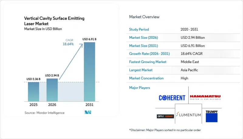
Mordor Intelligence에 의하면, 수직 공진 표면 발광 레이저(VCSEL) 시장 규모는 2026년에 29억 4,000만 달러로 추정되고, 2031년까지 69억 1,000만 달러에 이를 전망이며, CAGR 18.64%를 나타낼 것으로 예측됩니다.
본 보고서는 파장별(적색, 근적외선, 단파장 적외선), 다이 크기별(0.02-0.06 mm², 0.06-0.4 mm², 0.4-1.3 mm², 1.0-7.5 mm²), 최종 사용자 산업별(통신, 모바일·소비자, 자동차, 의료, 산업, 항공우주 및 방위), 용도별(데이터 통신, 홍채 스캔, ADAS LiDAR 등), 그리고 지역별로 분류되어 있습니다. 시장 예측은 금액(달러) 기준으로 제시되어 있습니다.
세계의 수직 공진 표면 발광 레이저(VCSEL) 시장 동향 및 인사이트
AI 최적화 하이퍼스케일 데이터센터에서 VCSEL 기반 광 링크 채택이 급증
하이퍼스케일 사업자들은 기존 클라우드 워크로드보다 4.2배 빠르게 증가하는 이스트-웨스트 트래픽에 대응하기 위해 100기가비트 레인에서 200기가비트 레인으로의 업그레이드를 추진하고 있습니다. 현재 2차원 64 이미터 어레이는 모듈당 1.6테라비트의 처리량을 실현하고 있으며, 실리콘 포토닉스 방식에 비해 기가비트당 트랜시버 비용을 18% 절감하고 테라비트당 전력 소비를 3.8와트로 낮추고 있습니다. 프론트 패널 모듈 대신 스위치 ASIC 위에 VCSEL 다이를 실장한 코패키지형 광 모듈이 보급되고 있으며, 이로 인해 홉 지연이 12나노초 단축되어 단거리 멀티모드 링크의 도입이 확대되고 있습니다. Microsoft Azure를 비롯한 각 공급업체들이 전력 사용 효율(PUE)을 1.15 미만으로 억제하는 것을 목표로 하는 가운데, VCSEL의 효율적 우위가 수직 공진기 표면 발광 레이저(VCSEL) 시장의 성장을 뒷받침하고 있습니다. CHIPS법에 따른 보조금으로 자금을 조달한 자본 집약형 팹은 현지 공급 안정성을 확보하는 동시에 제품 인증 주기를 가속화하고 있습니다.
플래그십 및 중급형 스마트폰에 3D 센싱용 VCSEL 어레이의 급속한 통합
각 스마트폰 제조업체들은 940나노미터 플러드 일루미네이터를 400달러 미만의 단말기에 탑재하고 있으며, 2024년부터 2027년까지 해당 단말기 수는 2배로 증가할 전망입니다. 새로운 도트 프로젝터는 피크 출력이 1.2와트를 초과하면서도, 밝은 햇빛 아래에서도 0.4초 미만에 얼굴 인식을 가능하게 합니다. 2.4mm × 3.2mm 크기의 소형 모놀리식 모듈을 통해 기판 공간을 34% 절감하여, 폴더블 힌지 및 웨어러블 기기에 쉽게 적용할 수 있게 되었습니다. 심도 맵의 품질은 기기상의 AR 필터 및 제스처 내비게이션을 지원하는 한편, 자동차용 실내 카메라와의 업계 전반에 걸친 대량 생산을 통해 다이 비용이 연간 0.14달러 절감되었습니다. 다양한 이용 사례 덕분에 스마트폰 출하량이 정체된 상황에서도 수직 공진 표면 발광 레이저(VCSEL) 시장은 두 자릿수 성장을 유지하고 있습니다.
InP 기반 VCSEL 에피택시에서 수율이 낮아 장파장 제품공급이 제한되고 있습니다.
인듐 인화물(InP) 웨이퍼의 결함 밀도는 여전히 갈륨 비소(GaAs)의 2.3배로 높아, 이로 인해 수율이 저하되고,다이 비용을 940나노미터 상당 제품보다 1.80달러 높게 유지시키고 있어, 가격에 민감한 소비자용 기기 시장에는 부담이 되고 있습니다. 3인치 웨이퍼의 기판 가격은 평균 420달러이지만, 금속 유기 화학 기상 증착(MOCVD) 장비의 가동률은 고작 68%에 그치고 있어, 규모의 경제와는 거리가 먼 상황입니다. 4,800만 달러 규모의 확장 계획은 2027년 하반기까지 완전 생산에 도달하지 못할 전망이며, 이로 인해 디스플레이 내장 센서 및 장거리 데이터 통신 링크용 공급 부족이 장기화될 것으로 보입니다. 이러한 병목 현상으로 인해, 본래라면 견조한 성장이 예상되던 수직 공진기 표면 발광 레이저(VCSEL) 시장의 성장이 일시적으로 저해되고 있습니다.
부문 분석
750나노미터에서 1,400나노미터 범위의 근적외선 디바이스는 2025년에 매출의 56.72%를 차지했으며, 데이터 통신용 트랜시버와 스마트폰의 심도 카메라에 있어 핵심 부문으로 자리 잡고 있습니다. 1,400나노미터에서 3,000나노미터의 파장 범위를 가진 단파장 적외선 이미터는 IEC 60825 규격의 제한이 완화되어 10배 더 높은 광 출력이 허용됨에 따라 연평균 성장률(CAGR) 19.37%로 확대되고 있습니다. 이는 망막에 대한 위험 경고를 발령하지 않고도 1.2미터를 넘는 범위를 스캔해야 하는 차량 내 모니터링 시스템에 획기적인 변화를 가져오고 있습니다.
Lumentum에 따르면, 2025년 단파장 적외선 제품 출하량은 전년 대비 34% 증가를 기록했으며, 자동차 업계의 Tier 1 공급업체들은 1,550나노미터 어레이를 헤드업 디스플레이에 통합하고 있습니다. 광학 마우스가 정전용량식 인터페이스로 대체됨에 따라, 750나노미터 미만의 적색 파장은 계속해서 감소 추세를 보이고 있습니다. 공급망은 양극화되고 있습니다. 갈륨 비소 팹은 850나노미터 및 940나노미터의 대량 주문을 우선시하는 반면, 인듐 인화물 전문 제조업체들은 자동차 및 의료 분야의 수익성을 추구하고 있으며, 이 모든 것이 종합적으로 수직 공진기 표면 발광 레이저(VCSEL) 시장을 재편하고 있습니다.
0.06-0.4 mm2의 실적는 스마트폰 내부의 열 부하와 얼굴 인식 성능의 균형을 맞추고 있어, 2025년에는 39.14%의 점유율을 차지했습니다. 200미터 LiDAR에 필요한 8kW/cm2의 복사 조도 임계값을 충족하기 위해, 1.0-7.5mm2 크기의 제품은 19.61%라는 놀라운 연간 성장률을 기록하고 있습니다. 이러한 성장은 자율주행차, 로봇 공학, 첨단 매핑 기술 등 정확하고 효율적인 감지 능력이 필수적인 분야에서 고성능 LiDAR 시스템에 대한 수요가 증가함에 따라 주도되고 있습니다.
ams OSRAM은 현재 중형 승용차용으로 피크 출력 100와트에 달하는 3.5 mm²의 다중 접합 어레이를 출하하고 있습니다. TRUMPF의 7.2 mm2 다이는 400와트의 버스트 출력을 입증했지만, 듀티 사이클이 0.8%로 제한되어 있었기 때문에 마이크로채널 냉각 프로그램의 도입이 진행되고 있습니다. 다이 면적이 클수록 수율이 중형 크기의 88%에 비해 72%로 떨어지기 때문에 제조 라인 분석을 통해 불량품을 줄여야 합니다. 이러한 규모의 변화는 ADAS의 보급이 수직 공진 표면 발광 레이저(VCSEL) 시장의 수익 구조를 어떻게 재편하고 있는지를 여실히 보여줍니다.
지역별 분석
2025년, 아시아태평양은 35.77%라는 압도적인 점유율을 차지했습니다. 이는 대만 및 일본의 에피택셜 팹이 82%라는 놀라운 가동률을 유지하고 있는 데 힘입은 결과입니다. 이러한 견실한 성과는 제조 능력의 발전과 최첨단 기술에 대한 꾸준한 수요에 힘입은 것으로, 해당 지역이 세계 반도체 시장에서 지극히 중요한 역할을 하고 있음을 여실히 보여줍니다. 한편, 중국은 화합물 반도체 펀드에 280억 위안을 투자하여 2027년까지 850나노미터 및 940나노미터 기술의 자급자족을 전략적으로 목표로 하고 있습니다. 이는 수입 의존도를 낮추고 국내 반도체 생태계를 강화하려는 중국의 노력을 반영한 것입니다.
Coherent와 Lumentum은 북미에서 사업 확장을 추진하고 있으며, 그 배경에는 ‘CHIPS법’에 따른 18억 달러의 보조금이 있습니다. 이 보조금은 보다 안정적이고 안전한 공급망을 확보함으로써 하이퍼스케일러공급 리스크를 완화하기 위한 것입니다. 이 자금은 하이퍼스케일 데이터센터에 필수적인 첨단 포토닉스 기술 개발을 지원하고 있습니다. 한편, 독일의 포토닉스 벨트를 중심으로 한 유럽은 자동차 업계의 Tier 1 공장에 인접해 있다는 입지 조건의 혜택을 누리고 있습니다. 이를 통해 VCSEL의 리드타임이 14주에서 불과 9주로 단축될 뿐만 아니라, 주요 자동차 제조업체와의 협업 기회도 확대되어 포토닉스 용도 분야의 혁신이 촉진되고 있습니다.
사우디아라비아와 UAE의 하이퍼스케일 캠퍼스에 대한 국부펀드의 투자가 증가하고 있으며, 중동 및 아프리카에서는 연평균 성장률(CAGR)이 19.73%를 나타낼 것으로 예측됩니다. 이러한 투자는 지역 기술력 향상에 필수적인 현지화된 대규모 언어 모델 훈련을 지원하는 것을 목적으로 합니다. 또한, 지리적 분산화는 정치적 공급망 위험을 완화하는 데 중요한 역할을 수행하고 있으며, 이를 통해 전 세계 수직 공진기 표면 발광 레이저(VCSEL) 시장을 강화하고 지정학적 불확실성에 대한 회복력을 확보하고 있습니다.
기타 혜택 :
- 엑셀 형식 시장 예측(ME) 시트
- 3개월간 애널리스트 지원
자주 묻는 질문
목차
제1장 서론
제2장 조사 방법
제3장 주요 요약
제4장 시장 구도
제5장 시장 규모 및 성장 예측
제6장 경쟁 구도
제7장 시장 기회 및 향후 전망
AJY 26.09.07According to Mordor Intelligence, the vertical cavity surface-emitting laser market size was USD 2.94 billion in 2026 and is projected to reach USD 6.91 billion by 2031, growing at an 18.64% CAGR.
This report is Segmented by Wavelength (Red, Near-Infrared, Shortwave-Infrared), Die Size (0. 02-0. 06 Mm2, 0. 06-0. 4 Mm2, 0. 4-1. 3 Mm2, 1. 0-7. 5 Mm2), End-User Industry (Telecom, Mobile and Consumer, Automotive, Medical, Industrial, Aerospace and Defense), Application (Datacom, Iris Scan, ADAS LiDAR, and More), and Geography. The Market Forecasts are Provided in Terms of Value (USD).
Global Vertical Cavity Surface Emitting Laser Market Trends and Insights
Surging Adoption of VCSEL-Based Optical Links in AI-Optimized Hyperscale Data Centers
Hyperscale operators are upgrading from 100 gigabit to 200 gigabit lanes to satisfy east-west traffic that scales 4.2 times faster than traditional cloud workloads. Two-dimensional 64-emitter arrays now deliver 1.6 terabit throughput per module, reducing transceiver cost by 18% per gigabit and lowering power draw to 3.8 watts per terabit compared to silicon-photonics alternatives. Front-panel modules are giving way to co-packaged optics that seat VCSEL dies on switch ASICs, cutting hop latency by 12 nanoseconds and driving preference for short-reach multimode links. As Microsoft Azure and other providers strive to achieve power-usage-effectiveness ratios below 1.15, the efficiency advantage of VCSELs bolsters the vertical cavity surface-emitting laser market. Capital-intensive fabs funded by CHIPS Act grants ensure local supply security and accelerate product qualification cycles.
Rapid Integration of 3D Sensing VCSEL Arrays in Flagship and Mid-Tier Smartphones
Smartphone brands have pushed 940-nanometer flood illuminators into devices priced under USD 400, doubling the addressable unit base between 2024 and 2027. New dot projectors exceed 1.2 watts peak power yet unlock faces in under 0.4 seconds under bright sunlight. Compact 2.4 mm X 3.2 mm monolithic modules shave 34% board space, easing adoption in foldable hinges and wearables. Depth-map quality supports on-device AR filters and gesture navigation, while cross-industry volumes with automotive cabin cameras erode die cost by USD 0.14 annually. The use case breadth sustains double-digit growth for the vertical cavity surface-emitting laser market, even as overall smartphone shipments plateau.
Limited Yield for InP-Based VCSEL Epitaxy Constrains Long-Wave Supply
Defect densities in indium phosphide wafers remain 2.3 times higher than those in gallium arsenide, suppressing yield and keeping die costs USD 1.80 above those of 940-nanometer equivalents, a burden for price-sensitive consumer gadgets. Substrate prices average USD 420 for a 3-inch wafer, while metal-organic chemical vapor deposition reactors run at only 68% utilization, far from scale economies. Planned expansions worth USD 48 million will not reach full output until late 2027, prolonging shortages for under-display sensors and long-reach datacom links. The bottleneck temporarily hinders the otherwise robust growth of the vertical cavity surface-emitting laser market.
Other drivers and restraints analyzed in the detailed report include:
- Transition to Long-Wavelength 1.3 µm VCSELs Enabling Under-Display Biometric Modules
- Multi-Junction VCSELs Powering High-Resolution Solid-State LiDAR for ADAS
- Short Optical Reach Versus Silicon Photonics in Next-Generation Data Centers
For complete list of drivers and restraints, kindly check the Table Of Contents.
Segment Analysis
Near-infrared devices, ranging from 750 nanometers to 1,400 nanometers, controlled 56.72% of the revenue in 2025, an anchor segment for datacom transceivers and smartphone depth cameras. Shortwave-infrared emitters between 1,400 nanometers and 3,000 nanometers are expanding at a 19.37% CAGR due to looser IEC 60825 limits that allow 10 times higher optical power, a game-changer for cabin monitoring systems that must scan beyond 1.2 meters without triggering retinal-hazard warnings.
Lumentum documented 34% year-over-year growth in shortwave-infrared shipments in 2025, with automotive tier-1 suppliers integrating 1,550-nanometer arrays into head-up displays. Red wavelengths below 750 nanometers continue to fade as optical mice give way to capacitive interfaces. Bifurcated supply chains emerge: gallium arsenide fabs prioritize high-volume orders for 850 nanometer and 940 nanometer, while indium phosphide specialists chase automotive and medical margins, collectively reshaping the vertical cavity surface-emitting laser market.
The footprints of 0.06-0.4 mm2 held a 39.14% share in 2025, as they balance thermal load with facial-recognition performance inside smartphones. To meet the 8 kW/cm2 irradiance threshold required for a 200-meter LiDAR, formats ranging from 1.0 to 7.5 mm2 are witnessing an impressive annual growth rate of 19.61%. This growth is driven by the increasing demand for high-performance LiDAR systems in applications such as autonomous vehicles, robotics, and advanced mapping technologies, where precise and efficient sensing capabilities are critical.
ams OSRAM now ships 3.5 mm2 multi-junction arrays that reach 100-watt peaks for mid-range passenger cars. TRUMPF's 7.2 mm2 dies demonstrated 400-watt bursts, although limited to 0.8% duty cycles, prompting the implementation of microchannel cooling programs. Larger die areas yield 72% versus 88% for mid-sizes, prompting fabrication-line analytics to mitigate scrap. The scale shift highlights how ADAS adoption reconfigures revenue pools within the vertical cavity surface-emitting laser market.
Complete Report Scope:
- By Wavelength
- Red (650-750 nm)
- Near-Infrared (750-1400 nm)
- Shortwave-Infrared (1400-3000 nm)
- By Die Size
- 0.02 - 0.06 mm2
- 0.06 - 0.4 mm2
- 0.4 - 1.3 mm2
- 1.0 - 7.5 mm2
- By End-User Industry
- Telecom
- Mobile and Consumer
- Automotive
- Medical
- Industrial
- Aerospace and Defense
- By Application
- Datacom
- Facial Recognition and Depth Camera
- Gesture Recognition
- Proximity Sensing
- Laser Autofocus
- Iris Scan
- Medical Diagnostics
- ADAS LiDAR
- Industrial Processing
- Optical Mouse
- Other Application
- By Geography
- North America
- United States
- Canada
- Mexico
- Europe
- Germany
- United Kingdom
- France
- Russia
- Rest of Europe
- Asia-Pacific
- China
- Japan
- India
- South Korea
- Australia
- Rest of Asia-Pacific
- Middle East and Africa
- Middle East
- Saudi Arabia
- United Arab Emirates
- Rest of Middle East
- Africa
- South Africa
- Egypt
- Rest of Africa
- Middle East
- South America
- Brazil
- Argentina
- Rest of South America
- North America
Geography Analysis
In 2025, the Asia-Pacific region commanded a dominant 35.77% share, buoyed by Taiwanese and Japanese epitaxial fabs running at an impressive 82% utilization rate. This strong performance highlights the region's pivotal role in the global semiconductor market, driven by advancements in manufacturing capabilities and robust demand for cutting-edge technologies. Meanwhile, China's CNY 28 billion investment in its compound semiconductor fund is strategically targeting self-sufficiency in 850-nanometer and 940-nanometer technologies by 2027, reflecting the country's commitment to reducing reliance on imports and strengthening its domestic semiconductor ecosystem.
Coherent and Lumentum have expanded in North America, bolstered by USD 1.8 billion in CHIPS Act grants, which mitigate supply risks for hyperscalers by ensuring a more stable and secure supply chain. This funding supports the development of advanced photonics technologies critical for hyperscale data centers. Meanwhile, Europe, centered in Germany's photonics belt, benefits from its closeness to automotive tier-1 plants, which not only reduces VCSEL lead times from 14 weeks to just 9 but also enhances collaboration opportunities with key automotive manufacturers, fostering innovation in photonics applications.
Sovereign funds are increasingly investing in hyperscale campuses in Saudi Arabia and the UAE, driving a projected 19.73% CAGR in the Middle East and Africa. These investments aim to support the training of localized large-language models, which are critical for advancing regional technological capabilities. Additionally, geographic diversification is playing a key role in mitigating political supply chain risks, thereby strengthening the global vertical cavity surface-emitting laser market and ensuring its resilience against geopolitical uncertainties.
- Coherent Corporation
- Lumentum Operations LLC
- ams OSRAM AG
- TRUMPF Group
- Broadcom Inc.
- Hamamatsu Photonics KK
- HLJ Technology Co. Ltd
- Teledyne FLIR Systems Inc.
- Vertilite Inc.
- Leonardo Electronics US
- Santec Corporation
- IQE plc
- WIN Semiconductors Corp.
- Bandwidth10 Inc.
- VERTILAS GmbH
- Ushio America Inc.
- Inneos LLC
- Frankfurt Laser Company
- Alight Technologies ApS
Additional Benefits:
- The market estimate (ME) sheet in Excel format
- 3 months of analyst support
TABLE OF CONTENTS
1 INTRODUCTION
- 1.1 Study Assumptions and Market Definition
- 1.2 Scope of the Study
2 RESEARCH METHODOLOGY
3 EXECUTIVE SUMMARY
4 MARKET LANDSCAPE
- 4.1 Market Overview
- 4.2 Market Drivers
- 4.2.1 Surging Adoption of VCSEL-Based Optical Links in AI-Optimized Hyperscale Data Centers
- 4.2.2 Rapid Integration of 3D Sensing VCSEL Arrays in Flagship and Mid-Tier Smartphones
- 4.2.3 Transition to Long-Wavelength (1.3 µm) VCSELs Enabling Under-Display Biometric Modules
- 4.2.4 Multi-Junction VCSELs Powering High-Resolution Solid-State LiDAR for ADAS
- 4.2.5 GaN-on-Si VCSEL Platforms Lowering Cost per Emitter and Expanding Visible-Light Markets
- 4.2.6 Government-Backed Semiconductor Reshoring Incentives Accelerating New VCSEL Fabs
- 4.3 Market Restraints
- 4.3.1 Limited Yield for InP-Based VCSEL Epitaxy Constrains Long-Wave Supply
- 4.3.2 Short Optical Reach Versus Silicon Photonics in Next-Gen Data-Center Architectures
- 4.3.3 IP Concentration Raises Licensing Costs for Emerging VCSEL Suppliers
- 4.3.4 Tight Eye-Safety Regulations Cap Output Power in Automotive Cabin Applications
- 4.4 Industry Value Chain Analysis
- 4.5 Regulatory Landscape
- 4.6 Technological Outlook
- 4.7 Porter's Five Forces Analysis
- 4.7.1 Bargaining Power of Suppliers
- 4.7.2 Bargaining Power of Buyers
- 4.7.3 Threat of New Entrants
- 4.7.4 Threat of Substitutes
- 4.7.5 Intensity of Competitive Rivalry
- 4.8 Impact of Macroeconomic Factors on the Market
- 4.9 Patent Landscape
- 4.10 Material Trend Analysis
5 MARKET SIZE AND GROWTH FORECASTS (VALUE)
- 5.1 By Wavelength
- 5.1.1 Red (650-750 nm)
- 5.1.2 Near-Infrared (750-1400 nm)
- 5.1.3 Shortwave-Infrared (1400-3000 nm)
- 5.2 By Die Size
- 5.2.1 0.02 - 0.06 mm2
- 5.2.2 0.06 - 0.4 mm2
- 5.2.3 0.4 - 1.3 mm2
- 5.2.4 1.0 - 7.5 mm2
- 5.3 By End-User Industry
- 5.3.1 Telecom
- 5.3.2 Mobile and Consumer
- 5.3.3 Automotive
- 5.3.4 Medical
- 5.3.5 Industrial
- 5.3.6 Aerospace and Defense
- 5.4 By Application
- 5.4.1 Datacom
- 5.4.2 Facial Recognition and Depth Camera
- 5.4.3 Gesture Recognition
- 5.4.4 Proximity Sensing
- 5.4.5 Laser Autofocus
- 5.4.6 Iris Scan
- 5.4.7 Medical Diagnostics
- 5.4.8 ADAS LiDAR
- 5.4.9 Industrial Processing
- 5.4.10 Optical Mouse
- 5.4.11 Other Application
- 5.5 By Geography
- 5.5.1 North America
- 5.5.1.1 United States
- 5.5.1.2 Canada
- 5.5.1.3 Mexico
- 5.5.2 Europe
- 5.5.2.1 Germany
- 5.5.2.2 United Kingdom
- 5.5.2.3 France
- 5.5.2.4 Russia
- 5.5.2.5 Rest of Europe
- 5.5.3 Asia-Pacific
- 5.5.3.1 China
- 5.5.3.2 Japan
- 5.5.3.3 India
- 5.5.3.4 South Korea
- 5.5.3.5 Australia
- 5.5.3.6 Rest of Asia-Pacific
- 5.5.4 Middle East and Africa
- 5.5.4.1 Middle East
- 5.5.4.1.1 Saudi Arabia
- 5.5.4.1.2 United Arab Emirates
- 5.5.4.1.3 Rest of Middle East
- 5.5.4.2 Africa
- 5.5.4.2.1 South Africa
- 5.5.4.2.2 Egypt
- 5.5.4.2.3 Rest of Africa
- 5.5.4.1 Middle East
- 5.5.5 South America
- 5.5.5.1 Brazil
- 5.5.5.2 Argentina
- 5.5.5.3 Rest of South America
- 5.5.1 North America
6 COMPETITIVE LANDSCAPE
- 6.1 Market Concentration
- 6.2 Strategic Moves
- 6.3 Market Share Analysis
- 6.4 Company Profiles (includes Global Level Overview, Market Level Overview, Core Segments, Financials as available, Strategic Information, Market Rank/Share for Key Companies, Products and Services, and Recent Developments)
- 6.4.1 Coherent Corporation
- 6.4.2 Lumentum Operations LLC
- 6.4.3 ams OSRAM AG
- 6.4.4 TRUMPF Group
- 6.4.5 Broadcom Inc.
- 6.4.6 Hamamatsu Photonics KK
- 6.4.7 HLJ Technology Co. Ltd
- 6.4.8 Teledyne FLIR Systems Inc.
- 6.4.9 Vertilite Inc.
- 6.4.10 Leonardo Electronics US
- 6.4.11 Santec Corporation
- 6.4.12 IQE plc
- 6.4.13 WIN Semiconductors Corp.
- 6.4.14 Bandwidth10 Inc.
- 6.4.15 VERTILAS GmbH
- 6.4.16 Ushio America Inc.
- 6.4.17 Inneos LLC
- 6.4.18 Frankfurt Laser Company
- 6.4.19 Alight Technologies ApS
7 MARKET OPPORTUNITIES AND FUTURE OUTLOOK
- 7.1 White-Space and Unmet-Need Assessment


