

|
시장보고서
상품코드
2122639
웨이퍼 세정 장비 시장 : 시장 점유율 분석, 업계 동향 및 통계, 성장 예측(2026-2031년)Wafer Cleaning Equipment - Market Share Analysis, Industry Trends & Statistics, Growth Forecasts (2026 - 2031) |
||||||
 Mordor Intelligence
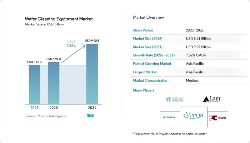
Mordor Intelligence에 의하면, 웨이퍼 세정 장비 시장 규모는 2025년에 64억 2,000만 달러로 평가되었고, 2026년 69억 1,000만 달러에서 2031년까지 99억 2,000만 달러에 이를 것으로 예측되며, 예측 기간(2026-2031년) CAGR은 7.52%를 나타낼 전망입니다.
본 보고서는 운영 모드별(자동 장비 등), 기술 유형별(싱글 웨이퍼 스프레이, 싱글 웨이퍼 극저온 세정 등), 웨이퍼 크기별(150mm 이하, 200mm, 300mm, 450mm 이상), 용도별(스마트폰·태블릿, 메모리 디바이스 등), 최종 사용자별(파운드리, IDM, OSAT), 지역별(북미, 유럽, 아시아태평양, 남미, 중동 및 아프리카)로 분류되어 있습니다.
세계의 웨이퍼 세정 장비 시장 동향 및 인사이트
3D NAND의 보급과 DRAM의 미세화가 진행되면서, 결함 없는 FEOL 세정에 대한 수요가 증가하고 있습니다.
2030년까지 1,000층 3D NAND를 실현하기 위한 양산 로드맵에서는 층이 1층 늘어날 때마다 입자로 인한 수율 저하가 발생하기 때문에 세정 공정이 두 배로 증가하고 있습니다. SK하이닉스는 2028년까지의 메모리 미세화를 위해 750억 달러를 계상했으며, 그 중 80%를 고대역폭 메모리에 할당하고 있습니다. 램 리서치(Lam Research)는 딥 트렌치 내의 폴리머 잔류물을 줄이기 위해 ‘Cryo 3.0’ 에칭 공정을 도입했습니다. 서브옹스트롬 수준의 제거 정밀도를 실현하는 장비 제조업체들은 층수 증가의 혜택을 누리고 있으며, 웨이퍼 세정 장비 시장을 주도하고 있습니다. 현재 메모리 제조 공장에서는 10nm 미만에서 검증된 제거 효율을 조건으로 장비 구매 계약을 체결하고 있어, 장기적인 수요가 더욱 강화되고 있습니다.
미국, 한국, 대만의 파운드리 생산 능력 확대가 새로운 장비 도입 기반을 창출하고 있습니다.
CHIPS법에 따라 애리조나주에서 대규모 장비 조달이 이루어졌습니다. 해당 주에 위치한 TSMC의 복합 시설에는 수천 대의 공정 장비가 필요합니다. Samsung Electronics와 SK하이닉스는 2047년까지 16개의 신규 팹 건설에 622조 원(4,710억 달러)을 투자하겠다고 밝혔으며, 당분간 수주 사이클이 활발해지고 있습니다. 도쿄 일렉트론은 차세대 비즈니스 기회를 확보하기 위해 5년간 연구개발비를 1조 5,000억 엔으로 거의 두 배로 늘렸습니다. 생산 능력 확충은 3nm 이하에 중점을 두고 있으며, 그 결과 첨단 웨이퍼 세정 장비 시장에 진입한 기업만이 충족할 수 있는 사양이 요구되고 있습니다. 장비의 납기 기간이 짧고 서비스 거점이 인접해 있다는 점이 완전 자동 세정 플랫폼의 수주를 즉시 급증시켰습니다.
불소계 온실가스(F-GHG)에 대한 엄격한 배출 규제
세계 반도체 업계는 PFOA의 단계적 폐지를 약속함에 따라, 사용 가능한 화학물질의 선택지가 좁아지고 있습니다. 미국 환경보호청(EPA)의 PFAS 심사 가속화는 화학 물질 로드맵에 불확실성을 초래하고 있습니다. 유럽의 팹에서는 주로 배출 저감 모듈을 사후 장착함으로써 2010년부터 2020년에 걸쳐 PFC 배출량을 42% 감축했습니다. 현재 장비 제조업체들은 스크러버와 폐쇄형 화학물질 재활용 장비를 세트로 판매하고 있으며, 이로 인해 도입 비용이 상승하고 투자 회수 기간(ROI)이 장기화되면서 웨이퍼 세정 장비 시장의 성장 전망은 둔화되고 있습니다.
부문 분석
최첨단 로직 라인의 엄격한 오염 관리 요건으로 인해 2025년 매출의 73.88%를 완전 자동화 플랫폼이 차지했으며, 웨이퍼 세정 장비 시장은 ‘자동화 우선’ 패러다임으로 전환되었습니다. 반자동 장비는 연구 개발(R&D)용 클린룸에서 계속 사용되고 있으며, 수동 시스템은 특수한 공정이나 구식 공정에만 국한되어 있습니다. 이미 지배적인 위치를 차지하고 있는 완전 자동화 부문은 AI를 활용한 레시피 최적화를 배경으로 연평균 8.14%의 복합 성장률로 확대될 것으로 예측됩니다. SCREEN사의 SS-3200 스핀 스크러버는 시간당 500장의 웨이퍼를 처리하면서 탈이온수 사용량을 줄이고, 장비 교체 주기를 뒷받침하고 있습니다.
장비 컨트롤러에 내장된 공정 분석 기능은 현재 로트당 수백만 개의 데이터 포인트를 저장하고 있어, 팹은 이상 현상을 예측하고 라인 정지를 사전에 방지할 수 있게 되었습니다. 각 벤더사는 노즐 오염이나 유량 불안정을 경고하는 예측 유지보수 모듈을 탑재하고 있습니다. 이러한 디지털 워크플로는 스마트 제조의 요건과 부합하며, 프리미엄 가격 책정을 뒷받침하고 있습니다. 그 결과, 웨이퍼 세정 장비 시장에서는 구매 결정 기준이 자본 지출(CAPEX)에서 가동률 지표 및 절수 효과를 기반으로 한 총 소유 비용(TCO)으로 전환되고 있습니다.
CAGR 스크러버는 화학 약품만으로는 해결할 수 없는 블랭킷 산화막 제거 작업을 담당했습니다.
도쿄 일렉트론의 극저온 에칭은 CO2 배출량을 80% 감축하여 친환경 화학(Green Chemistry)을 뒷받침했습니다. ACM Research사의 ‘Ultra C Tahoe’는 기존 성능을 유지하면서 황산 사용량을 75% 줄였으며, 여러 파운드리로 도입되었습니다. 현재 기술적 의사 결정은 입자 수 사양과 마찬가지로 물 및 온실가스 지표를 중시하는 방향으로 바뀌고 있으며, 웨이퍼 세정 장비 시장에서 싱글 웨이퍼 기술 혁신의 전략적 중요성이 더욱 높아지고 있습니다.
지역별 분석
아시아태평양은 2025년 매출의 71.92%를 차지했으며, 대만, 한국, 중국에서의 클러스터 투자가 주도적인 역할을 했습니다. 이 3개국에서는 총 월간 770만 장 이상의 웨이퍼 세정 능력이 도입되었습니다. 가오슝과 신주에서 파운드리 확장이 단기적인 장비 도입을 뒷받침한 반면, 수출 규제 하에서 중국의 IDM이 급증하면서 국내 장비 도입이 촉진되었습니다.
북미의 점유율은 CHIPS법에 따른 보조금을 활용한 TSMC의 애리조나주 및 인텔의 오하이오주 투자로 인해 상승했습니다. 이 팹들에서는 미국에 기반을 둔 서비스 팀과 예비 부품 허브가 지정되어, 웨이퍼 세정 장비 시장공급업체 선정 동향에 변화를 가져왔습니다.
유럽은 특수 분야에서 주도적인 위치를 유지했습니다. 인피니온과 ST마이크로일렉트로닉스는 SiC 생산을 확대했으며, 네덜란드에서는 1,200만 유로를 투자해 ‘ChipNL 센터’를 설립하고 세정 및 계측 플랫폼의 공동 개발을 추진하고 있습니다. 자동차 분야 수요가 장비의 꾸준한 교체를 뒷받침하고 있습니다.
남미, 중동 및 아프리카에서는 조립 공장에서 수요가 점차 대두되고 있습니다. UAE와 브라질 정부의 인센티브는 여전히 현지 웨이퍼 세정 서비스가 필요한 백엔드 시설 유치를 목표로 하고 있으며, 이는 웨이퍼 세정 장비 시장의 장기적인 지리적 다각화를 시사합니다.
기타 혜택 :
- 엑셀 형식 시장 예측(ME) 시트
- 3개월간의 애널리스트 지원
자주 묻는 질문
목차
제1장 서론
제2장 조사 방법
제3장 주요 요약
제4장 시장 구도
제5장 시장 규모 및 성장 예측
제6장 경쟁 구도
제7장 시장 기회 및 향후 전망
AJY 26.09.09According to Mordor Intelligence, the wafer cleaning equipment market size was valued at USD 6.42 billion in 2025 and estimated to grow from USD 6.91 billion in 2026 to reach USD 9.92 billion by 2031, at a CAGR of 7.52% during the forecast period (2026-2031).
This report is Segmented by Operating Mode (Automatic Equipment, and More), Technology Type (Single-Wafer Spray, Single-Wafer Cryogenic, and More), Wafer Size (<=150 Mm, 200 Mm, 300 Mm, and >=450 Mm), Application (Smartphones and Tablets, Memory Devices, and More), End-User (Foundries, IDM, and OSAT), and Geography (North America, Europe, Asia-Pacific, South America, and Middle East and Africa).
Global Wafer Cleaning Equipment Market Trends and Insights
Proliferation of 3-D NAND and DRAM Node Shrinks Driving Defect-Free FEOL Cleaning Demand
Mass-production roadmaps toward 1,000-layer 3-D NAND by 2030 multiply cleaning steps because every additional layer increase particle-induced yield loss. SK Hynix earmarked USD 75 billion for memory scaling through 2028, directing 80% to high-bandwidth memory. Lam Research introduced Cryo 3.0 etch to mitigate polymer residues in deep trenches. Equipment makers that deliver sub-angstrom removal precision are benefiting from rising layer counts, lifting the wafer cleaning equipment market. Memory fabs now contractually link tool purchase decisions to demonstrated removal efficiency below 10 nm, reinforcing long-term demand.
Foundry Capacity Expansion in the U.S., Korea and Taiwan Creating New Tool Install Base
The CHIPS Act triggered large-scale tool procurement in Arizona, where TSMC's complex requires thousands of process tools. Samsung and SK Hynix committed 622 trillion won (USD 471 billion) for 16 new fabs by 2047, intensifying immediate order cycles. Tokyo Electron nearly doubled R&D spend to JPY 1.5 trillion over five years to secure next-generation opportunities. Capacity additions focus on 3 nm and below, translating to tool specs that only advanced wafer cleaning equipment market participants can meet. Short tool lead-times and service proximity drove an immediate surge in orders for fully automatic cleaning platforms.
Stringent Discharge Regulations on Fluorinated Greenhouse Gases (F-GHGs)
The global semiconductor industry pledged to phase out PFOA, tightening chemical options. The U.S. EPA's accelerated PFAS review injects uncertainty into chemistry roadmaps. European fabs cut PFC emissions 42% from 2010-2020, mainly by retrofitting abatement modules. Equipment firms now bundle scrubbers and closed-loop chemical recycle units, raising acquisition cost and extending ROI timelines, moderating the wafer cleaning equipment market growth projection.
Other drivers and restraints analyzed in the detailed report include:
- Transition Toward 300 mm SiC and GaN Power Wafers Requiring New Wet-Bench Chemistries
- Adoption of EUV Lithography Necessitating Ultra-Low Particle Cleans <10 nm
- Rising Ultrapure-Water (UPW) Cost in Drought-Prone Semiconductor Hubs
For complete list of drivers and restraints, kindly check the Table Of Contents.
Segment Analysis
Fully automatic platforms generated 73.88% of 2025 revenue thanks to strict contamination-control mandates on advanced logic lines, placing the wafer cleaning equipment market in an automation-first paradigm. Semi-automatic tools persisted in R&D cleanrooms, while manual systems stayed limited to specialty or legacy flows. The fully automatic segment, already dominant, is forecast to compound at 8.14% annually on the back of AI-driven recipe optimization. SCREEN's SS-3200 spin-scrubber processed 500 wafers per hour while cutting deionized-water use, underpinning replacement cycles.
Process analytics embedded in machine controllers now store millions of datapoints per lot, allowing fabs to predict excursions and prevent line stops. Vendors embed predictive-maintenance modules that flag nozzle fouling or flow instability. These digital workflows align with smart-manufacturing mandates, supporting premium pricing. Consequently, the wafer cleaning equipment market sees purchasing decisions shift from capex alone toward total cost-of-ownership anchored in uptime metrics and water savings.
Single-wafer spray lines earned 33.05% revenue share in 2025 by combining small footprint, chemistry savings, and recipe flexibility, helping maintain the wafer cleaning equipment market trajectory. Cryogenic CO2 variants, though newer, registered the fastest 11.64% CAGR outlook on the promise of near-zero liquid discharge. Batch immersion tools survived in high-volume commodity lines, while batch spray occupied the mid-tier. Scrubbers served blanket oxide removal tasks that chemicals alone could not address.
Tokyo Electron's cryogenic etch reduced CO2 emissions 80%, validating green-chemistry claims. ACM Research's Ultra C Tahoe slashed sulfuric-acid use 75% while matching legacy performance, winning multiple foundry installs. Technology decisions now revolve around water and greenhouse-gas metrics as much as particle-count specs, reinforcing the strategic importance of single-wafer innovation to the wafer cleaning equipment market.
Complete Report Scope:
- By Operating Mode
- Automatic Equipment
- Semi-automatic Equipment
- Manual Equipment
- By Technology Type
- Single-wafer Spray
- Single-wafer Cryogenic
- Batch Immersion
- Batch Spray
- Scrubbers
- By Wafer Size
- <=150 mm
- 200 mm
- 300 mm
- >=450 mm
- By Application
- Smartphones and Tablets
- Memory Devices
- RF Devices
- LED
- Power Discrete and IC
- CMOS Image Sensors
- By End-User
- Foundries
- Integrated Device Manufacturers (IDM)
- Outsourced Semiconductor Assembly and Test (OSAT)
- By Geography
- North America
- United States
- Canada
- Mexico
- Europe
- Germany
- France
- United Kingdom
- Nordics
- Rest of Europe
- Asia-Pacific
- China
- Taiwan
- South Korea
- Japan
- India
- Rest of Asia-Pacific
- South America
- Brazil
- Mexico
- Argentina
- Rest of South America
- Middle East and Africa
- Middle East
- Saudi Arabia
- United Arab Emirates
- Turkey
- Rest of Middle East
- Africa
- South Africa
- Rest of Africa
- Middle East
- North America
Geography Analysis
Asia-Pacific generated 71.92% of 2025 revenue, anchored by cluster investments in Taiwan, South Korea, and China that collectively installed more than 7.7 million wafers per month cleaning capacity. Foundry expansions in Kaohsiung and Hsinchu lifted near-term tool uptake, while China's IDM surge under export controls catalyzed domestic tool adoption.
North America's share rose on TSMC-Arizona and Intel's Ohio investments, leveraging CHIPS Act grants. These fabs specified US-based service teams and spare-parts hubs, altering vendor-selection dynamics inside the wafer cleaning equipment market.
Europe maintained specialty leadership: Infineon and STMicroelectronics expanded SiC output; the Netherlands launched the EUR 12 million ChipNL Centre to co-develop cleaning and metrology platforms. Automotive demand underpins steady tool renewal.
South America, and Middle East and Africa posted nascent demand from assembly plants. Government incentives in the UAE and Brazil aim to attract backend facilities that still need localized wafer cleaning services, hinting at longer-term geographic diversification for the wafer cleaning equipment market.
- SCREEN Semiconductor Solutions Co., Ltd.
- ACM Research Inc.
- MEI Wet Processing Systems & Services LLC
- Modutek Corporation
- Akrion Technologies LLC
- RENA Technologies GmbH
- JST Manufacturing Inc.
- Yield Engineering Systems (YES) Inc.
- AP&S International GmbH
- Semsysco GmbH
- MT Systems Co., Ltd.
- Expertech Systems Inc.
- Samco Inc.
- Naura Technology Group
- Applied Materials
- Tokyo Electron Limited (TEL)
- Kaijo Corporation
- Surpass Industry Co., Ltd.
- Kingsemi Co., Ltd.
- Hwatsing Technology Co., Ltd.
Additional Benefits:
- The market estimate (ME) sheet in Excel format
- 3 months of analyst support
TABLE OF CONTENTS
1 INTRODUCTION
- 1.1 Study Assumptions and Market Definition
- 1.2 Scope of the Study
2 RESEARCH METHODOLOGY
3 EXECUTIVE SUMMARY
4 MARKET LANDSCAPE
- 4.1 Market Overview
- 4.2 Market Drivers
- 4.2.1 Proliferation of 3-D NAND and DRAM node shrinks driving defect-free FEOL cleaning demand
- 4.2.2 Foundry capacity expansion in the U.S., Korea and Taiwan creating new tool install base
- 4.2.3 Transition toward 300 mm SiC and GaN power wafers requiring new wet-bench chemistries
- 4.2.4 Adoption of EUV lithography necessitating ultra-low particle cleans <10 nm
- 4.2.5 Rapid fab investments by Chinese IDMs despite U.S. export controls
- 4.3 Market Restraints
- 4.3.1 Stringent discharge regulations on fluorinated greenhouse gases (F-GHGs)
- 4.3.2 Rising ultrapure water (UPW) cost in drought-prone semiconductor hubs
- 4.3.3 High capex intensity versus alternative dry plasma cleans in BEOL
- 4.4 Value Chain Analysis
- 4.5 Regulatory and Technological Outlook
- 4.6 Porter's Five Forces Analysis
- 4.6.1 Threat of New Entrants
- 4.6.2 Bargaining Power of Buyers
- 4.6.3 Bargaining Power of Suppliers
- 4.6.4 Threat of Substitutes
- 4.6.5 Intensity of Competitive Rivalry
- 4.7 Investment Analysis
5 MARKET SIZE AND GROWTH FORECASTS (VALUE)
- 5.1 By Operating Mode
- 5.1.1 Automatic Equipment
- 5.1.2 Semi-automatic Equipment
- 5.1.3 Manual Equipment
- 5.2 By Technology Type
- 5.2.1 Single-wafer Spray
- 5.2.2 Single-wafer Cryogenic
- 5.2.3 Batch Immersion
- 5.2.4 Batch Spray
- 5.2.5 Scrubbers
- 5.3 By Wafer Size
- 5.3.1 <=150 mm
- 5.3.2 200 mm
- 5.3.3 300 mm
- 5.3.4 >=450 mm
- 5.4 By Application
- 5.4.1 Smartphones and Tablets
- 5.4.2 Memory Devices
- 5.4.3 RF Devices
- 5.4.4 LED
- 5.4.5 Power Discrete and IC
- 5.4.6 CMOS Image Sensors
- 5.5 By End-User
- 5.5.1 Foundries
- 5.5.2 Integrated Device Manufacturers (IDM)
- 5.5.3 Outsourced Semiconductor Assembly and Test (OSAT)
- 5.6 By Geography
- 5.6.1 North America
- 5.6.1.1 United States
- 5.6.1.2 Canada
- 5.6.1.3 Mexico
- 5.6.2 Europe
- 5.6.2.1 Germany
- 5.6.2.2 France
- 5.6.2.3 United Kingdom
- 5.6.2.4 Nordics
- 5.6.2.5 Rest of Europe
- 5.6.3 Asia-Pacific
- 5.6.3.1 China
- 5.6.3.2 Taiwan
- 5.6.3.3 South Korea
- 5.6.3.4 Japan
- 5.6.3.5 India
- 5.6.3.6 Rest of Asia-Pacific
- 5.6.4 South America
- 5.6.4.1 Brazil
- 5.6.4.2 Mexico
- 5.6.4.3 Argentina
- 5.6.4.4 Rest of South America
- 5.6.5 Middle East and Africa
- 5.6.5.1 Middle East
- 5.6.5.1.1 Saudi Arabia
- 5.6.5.1.2 United Arab Emirates
- 5.6.5.1.3 Turkey
- 5.6.5.1.4 Rest of Middle East
- 5.6.5.2 Africa
- 5.6.5.2.1 South Africa
- 5.6.5.2.2 Rest of Africa
- 5.6.5.1 Middle East
- 5.6.1 North America
6 COMPETITIVE LANDSCAPE
- 6.1 Market Concentration
- 6.2 Strategic Moves
- 6.3 Market Share Analysis
- 6.4 Company Profiles {(includes Global level Overview, Market level overview, Core Segments, Financials as available, Strategic Information, Market Rank/Share for key companies, Products and Services, and Recent Developments)}
- 6.4.1 SCREEN Semiconductor Solutions Co., Ltd.
- 6.4.2 ACM Research Inc.
- 6.4.3 MEI Wet Processing Systems & Services LLC
- 6.4.4 Modutek Corporation
- 6.4.5 Akrion Technologies LLC
- 6.4.6 RENA Technologies GmbH
- 6.4.7 JST Manufacturing Inc.
- 6.4.8 Yield Engineering Systems (YES) Inc.
- 6.4.9 AP&S International GmbH
- 6.4.10 Semsysco GmbH
- 6.4.11 MT Systems Co., Ltd.
- 6.4.12 Expertech Systems Inc.
- 6.4.13 Samco Inc.
- 6.4.14 Naura Technology Group
- 6.4.15 Applied Materials
- 6.4.16 Tokyo Electron Limited (TEL)
- 6.4.17 Kaijo Corporation
- 6.4.18 Surpass Industry Co., Ltd.
- 6.4.19 Kingsemi Co., Ltd.
- 6.4.20 Hwatsing Technology Co., Ltd.
7 MARKET OPPORTUNITIES AND FUTURE OUTLOOK
- 7.1 White-space and Unmet-Need Assessment


