|
시장보고서
상품코드
2122987
아웃소싱 반도체 조립 및 검사(OSAT) 시장 : 점유율 분석, 업계 동향과 통계, 성장 예측(2026-2031년)Outsourced Semiconductor Assembly And Test (OSAT) - Market Share Analysis, Industry Trends & Statistics, Growth Forecasts (2026 - 2031) |
||||||
 Mordor Intelligence
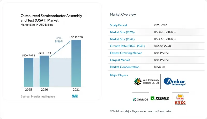
Mordor Intelligence에 의하면, 아웃소싱 반도체 조립 및 검사(OSAT) 시장 규모는 2025년에 470억 9,000만 달러로 평가되었고 2026년 511억 2,000만 달러에서 2031년까지 771억 2,000만 달러에 이를 것으로 예측되며, 예측 기간(2026-2031년) CAGR은 8.56%를 나타낼 전망입니다.
본 보고서는 서비스 유형(패키징 및 테스트), 패키지 유형(볼 그리드 어레이, 칩 스케일 패키지, 기타),용도(통신, 가전제품, 자동차, 컴퓨팅·네트워크, 기타), 기술 노드(28nm 이상, 16/14nm, 10/7nm, 기타), 지역(북미, 남미, 유럽, 아시아태평양, 중동 및 아프리카)에 따라 분류되어 있습니다.
전 세계 아웃소싱 반도체 조립 및 테스트(OSAT) 시장 동향 및 인사이트
대당 반도체 탑재량의 급증
자동차 OEM 업체들은 소프트웨어 정의 플랫폼으로의 전환을 추진하며, 차량당 반도체 부품표(BOM) 비용을 상승시키는 동시에 고신뢰성 패키지에 대한 수요를 높이고 있습니다. 폭스바겐 그룹과 온세미(onsemi)의 트랙션 인버터 제휴는 열적으로 견고한 파워 패키지가 필요한 실리콘 카바이드(SiC) 디바이스의 채택이 확대되고 있음을 여실히 보여주었습니다. ASE, BMW, Bosch가 지원하는 IMEC의 ‘Automotive Chiplet Program’은 기능 안전 규격 준수를 위한 표준화된 치플릿 패키징에 관한 밸류체인 전반에 걸친 협력을 보여줍니다. 그 결과, AEC-Q100 및 ISO 26262 인증을 획득한 OSAT 공급업체들은 새로운 설계 수주를 확보하고, 전기차 공급업체들과 수년에 걸친 생산 능력 확보에 성공했습니다.
5G에 힘입은 첨단 RF 패키지에 대한 수요
상용 5G 기지국의 확산에 따라 무선 프런트엔드는 mm파 영역으로 전환되었으며, 저손실 기판, 컨포멀 쉴드, 소형 SiP 실적가 필요하게 되었습니다. GlobalFoundries에서 Finwave Semiconductor의 E-모드 MISHEMT 집적화는 특수한 RF 패키지가 필요한 새로운 질화갈륨 디바이스의 상용화를 알리는 것으로, 2026년 양산 인증을 목표로 하고 있습니다. 6G 테스트베드 파이프라인에는 이미 코패키지드 옵틱스가 통합되어 있어, OSAT 기업들에게는 혼합 신호 조립 능력과 첨단 열 솔루션의 확충이 요구되고 있습니다.
대형 파운드리 및 IDM의 수직 통합
TSMC의 ‘Wafer Manufacturing 2.0’ 전략은 패키징 및 테스트 공정을 통합하고 턴키 서비스를 제공함으로써, 독립 OSAT 기업이 담당하는 생산량을 축소시켰습니다. 삼성도 비슷한 길을 걸었고, 인텔은 파운드리 서비스를 확대하여 첨단 인터포저를 도입했습니다. 이러한 움직임으로 인해 고수익 부문에서 제3자 업체의 점유율이 축소되었으며, OSAT 기업들은 자동차 안전 시스템이나 포토닉스와 같은 틈새 시장에 집중할 수밖에 없게 되었습니다.
부문 분석
테스트 부문은 2026년부터 2031년까지 연평균 성장률(CAGR) 10.35%를 나타낼 것으로 예측되며, 그 성장률은 패키징 부문의 성장률을 상회하지만 출발점은 더 낮습니다. AI 및 고성능 컴퓨팅(HPC) 설계에서는 칩렛 간의 상호 연결 지연, 동적 열 스로틀링, 다양한 전압 조건 하에서 딥러닝 워크로드의 성능을 검증하는 시스템 수준의 테스트 커버리지가 요구되었습니다. 이에 반해 OSAT 시장에서는 자동 테스트 장비에 적응형 머신러닝 알고리즘을 통합함으로써 테스트 시간을 단축하는 동시에 고장 부위 식별 정확도를 향상시켰습니다.
패키징 부문은 2025년 매출의 76.80%를 차지했으나, 그 구성은 팬아웃 패널 레벨, 2.5D 인터포저, 코패키지드 옵틱스 제품 라인으로 전환되었습니다. 고객이 공급업체를 통합하는 가운데, OSAT 각사는 픽스처 설계, 최종 테스트, 물류를 통합한 턴키 솔루션을 제공했습니다. Advantest는 V93000 시리즈에 AI를 활용한 분석 기능을 추가함으로써, 조립 테스트 장비 부문에서 6년 연속 1위를 유지했습니다.
볼 그리드 어레이(BGA) 기술은 기계적 견고성을 중시하는 주류 소비자용 및 산업용 플랫폼에 채택되어 2025년에도 23.85%의 점유율을 유지했습니다. 그러나 모바일 프로세서와 AI 가속기가 고밀도 재배선 층으로 전환됨에 따라, 팬아웃 웨이퍼 레벨 패키지는 연평균 성장률(CAGR) 11.02%로 성장할 전망입니다. 이러한 추세로 인해 OSAT 시장이 강화되었습니다. 이는 수율 변동을 초래하지 않으면서 대형 패널 형태를 처리할 수 있는 벤더가 제한적이기 때문입니다.
ASE가 2억 달러를 투자하여 310mm×310mm 유리 패널로 확대한 것은 비용 대비 효율이 높은 대면적 생산을 위한 설비 투자 의지를 보여주는 것입니다. 고대역폭 메모리 스택에서는 TSV(실리콘 관통 비아)와 TGV(유리 관통 비아)의 변형이 보급되었습니다. FC-BGA 기판은 첨단 노드 채택의 혜택을 받아, 네트워크용 ASIC에서 유기 라미네이트와 실리콘 인터포저 사이의 격차를 메우는 역할을 수행했습니다.
지역별 분석
아시아태평양은 2025년 OSAT 시장 매출에서 72.90%의 점유율을 유지할 것으로 보이며, 2031년까지의 연평균 성장률(CAGR)은 9.45%로 전망됩니다. 대만, 중국, 한국은 파운드리 및 기판 제조업체와의 근접성을 바탕으로 이 클러스터의 핵심을 담당해 왔으나, 무역 마찰이 심화됨에 따라 말레이시아, 베트남, 필리핀으로의 사업 다각화가 진행되었습니다. 인도는 인센티브 프로그램을 가속화하여 구자라트주에 위치한 Kaynes Technology의 4억 1,300만 달러 규모 공장과 아삼주에 위치한 Tata Electronics의 30억 달러 규모 패키징·테스트 복합 시설을 지원했습니다.
북미는 ‘CHIPS 법’에 따른 자금 지원을 받아 전략적 중요성을 회복했습니다. Amkor사는 국내 자동차 및 AI 고객에게 공급하기 위한 목적으로 애리조나주에 첨단 패키징 시설의 착공을 시작했습니다. Texas Instruments는 여러 웨이퍼 팹과 이에 상응하는 백엔드 생산 능력에 600억 달러를 배정하는 한편, SkyWater가 9,300만 달러에 Infineon의 오스틴 공장을 인수함으로써 국가 차원의 중복성을 높였습니다.
유럽은 틈새 연구개발에서 대규모 생산으로 전환했습니다. Silicon Box사는 이탈리아에 13억 유로(14억 7,000만 달러)를 투자해 패널 레벨 공장을 건설하는 데 대해 EU의 승인을 받았으며, 연간 1억 개 이상의 SiP(시스템 인 패키지) 생산을 목표로 하고 있습니다. Thales, Radiall, Foxconn은 방위 및 항공우주 부문의 고객에게 서비스를 제공하기 위해 프랑스 내 OSAT 제휴 구축을 검토했습니다. onsemi는 체코 공화국의 실리콘 카바이드(SiC) 생산 라인에 20억 달러를 투자하여 e-모빌리티 프로젝트를 위한 현지 공급을 확보했습니다. 중동 및 아프리카는 여전히 신흥 시장이며, 이스라엘과 아랍에미리트는 백엔드 투자자를 유치하기 위한 정책 프레임워크를 검토하고 있습니다.
기타 혜택
- 엑셀 형식 시장 예측(ME) 시트
- 3개월간 애널리스트 지원
자주 묻는 질문
목차
제1장 서론
제2장 조사 방법
제3장 주요 요약
제4장 시장 구도
제5장 시장 규모와 성장 예측
제6장 경쟁 구도
제7장 시장 기회와 향후 전망
JHS 26.09.09According to Mordor Intelligence, the outsourced semiconductor assembly and test market size was valued at USD 47.09 billion in 2025 and estimated to grow from USD 51.12 billion in 2026 to reach USD 77.12 billion by 2031, at a CAGR of 8.56% during the forecast period (2026-2031).
This report is Segmented by Service Type (Packaging, and Testing), Packaging Type (Ball Grid Array, Chip-Scale Package, and More), Application (Communication, Consumer Electronics, Automotive, Computing and Networking, and More), Technology Node (>=28 Nm, 16/14 Nm, 10/7 Nm, and More), and Geography (North America, South America, Europe, Asia-Pacific, and Middle East and Africa).
Global Outsourced Semiconductor Assembly And Test (OSAT) Market Trends and Insights
Soaring Semiconductor Content Per Vehicle
Automotive OEMs transitioned toward software-defined platforms, lifting semiconductor bill-of-materials per car and intensifying demand for high-reliability packages. Volkswagen Group's traction inverter partnership with onsemi highlighted the rising adoption of silicon carbide devices that need thermally robust power packages.Imec's Automotive Chiplet Program, supported by ASE, BMW, and Bosch, illustrated cross-value-chain alignment on standardized chiplet packaging for functional safety compliance. OSAT providers that qualify to AEC-Q100 and ISO 26262, therefore, captured new design wins and secured multiyear capacity reservations with electric-vehicle suppliers.
5G-Led Demand for Advanced RF Packages
Commercial 5G base-station roll-outs moved the radio front-end into millimetre-wave territory, necessitating low-loss substrates, conformal shielding, and compact SiP footprints. Finwave Semiconductor's E-mode MISHEMT integration at GlobalFoundries signalled commercial deployment of novel gallium-nitride devices that require specialised RF packaging, with mass qualification targeted for 2026. The pipeline for 6G testbeds already incorporates co-packaged optics, urging OSAT firms to expand mixed-signal assembly capabilities and advanced thermal solutions.
Vertical Integration by Leading Foundries and IDMs
TSMC's Wafer Manufacturing 2.0 strategy integrated packaging and testing flows, offering turnkey services that reduced addressable volume for stand-alone OSAT companies. Samsung pursued a similar path, while Intel grew its foundry services to include advanced interposers. These moves compressed third-party share in high-margin segments and obliged OSAT firms to double down on niches such as automotive safety or photonics.
Other drivers and restraints analyzed in the detailed report include:
- AI/HPC Chiplet Architectures Needing Heterogeneous Integration
- Foundry Capacity Shortages Driving Fab-Lite Outsourcing
- Cap-Ex Intensity and Long Equipment Lead-Times
For complete list of drivers and restraints, kindly check the Table Of Contents.
Segment Analysis
Testing captured a 10.35% CAGR forecast for 2026-2031, a pace outstripping packaging's expansion yet starting from a smaller base. AI and high-performance computing designs demanded system-level test coverage that verifies chiplet interconnect latency, dynamic thermal throttling, and deep-learning workload performance under varied voltages. The outsourced semiconductor assembly and test market responded by integrating adaptive machine-learning algorithms in automatic test equipment, cutting test time while improving fault isolation.
Packaging retained 76.80% of 2025 revenue, but its composition evolved toward fan-out panel-level, 2.5D interposer, and co-packaged optics lines. As customers consolidated suppliers, OSAT groups bundled turnkey offerings that merge fixture design, final test, and logistics. Advantest secured its sixth consecutive leadership in assembly test equipment after adding AI-enabled analytics to its V93000 series.
Ball grid array technology maintained a 23.85% share in 2025 by serving mainstream consumer and industrial platforms that value mechanical robustness. However, fan-out wafer-level packages expanded at 11.02% CAGR as mobile processors and AI accelerators transitioned to high-density redistribution layers. This trend strengthened the outsourced semiconductor assembly and test market because only a limited pool of vendors can process larger panel formats without yield drift.
ASE's USD 200 million panel-level expansion to 310 mm X 310 mm glass panels illustrated a cap-ex commitment toward cost-effective, large-area builds. Through-silicon-via and through-glass-via variants proliferated in high-bandwidth memory stacks. FC-BGA substrates benefited from advanced node adoption, bridging the gap between organic laminates and silicon interposers for networking ASICs.
Complete Report Scope:
- By Service Type
- Packaging
- Testing
- By Packaging Type
- Ball Grid Array (BGA)
- Chip-Scale Package (CSP)
- Quad Flat / Dual-Inline (QFP/DIP)
- Multi-Chip Module (MCM)
- Wafer-Level Packaging (WLP)
- Fan-Out Packaging (FO-WLP / FO-BGA)
- System-in-Package (SiP)
- Through-Silicon Via (2.5D/3D TSV)
- Flip-Chip (FC-BGA / FC-CSP)
- By Application
- Communication
- Consumer Electronics
- Automotive
- Computing and Networking
- Industrial
- Other Applications
- By Technology Node
- >=28 nm
- 16/14 nm
- 10/7 nm
- 5 nm and below
- Legacy (90-65 nm)
- By Geography
- North America
- United States
- Canada
- Mexico
- South America
- Brazil
- Argentina
- Rest of South America
- Europe
- Germany
- France
- United Kingdom
- Italy
- Netherlands
- Russia
- Rest of Europe
- Asia-Pacific
- China
- Taiwan
- South Korea
- Japan
- Singapore
- Malaysia
- India
- Rest of Asia-Pacific
- Middle East and Africa
- Middle East
- Israel
- United Arab Emirates
- Saudi Arabia
- Turkey
- Rest of Middle East
- Africa
- South Africa
- Nigeria
- Rest of Africa
- Middle East
- North America
Geography Analysis
Asia-Pacific retained 72.90% share of outsourced semiconductor assembly and test market revenue in 2025 and posted a 9.45% CAGR outlook through 2031. Taiwan, China, and South Korea anchored the cluster owing to proximity to foundries and substrate makers, yet escalating trade frictions prompted diversification into Malaysia, Vietnam, and the Philippines. India accelerated incentive programmes, endorsing Kaynes Technology's USD 413 million plant in Gujarat and Tata Electronics' USD 3 billion Assam package-test complex.
North America regained strategic weight following the CHIPS Act funding. Amkor broke ground on an advanced packaging facility in Arizona designed to supply domestic automotive and AI customers. Texas Instruments earmarked USD 60 billion for multiple wafer fabs and corresponding backend capacity, while SkyWater's USD 93 million acquisition of Infineon's Austin fab added sovereign redundancy.
Europe moved from niche R&D toward scaled production. Silicon Box obtained EU approval for a EUR 1.3 billion (USD 1.47 billion) panel-level plant in Italy, targeting >100 million SiP units per year. Thales, Radiall, and Foxconn explored a French OSAT alliance to serve defence and aeronautics users. Onsemi committed USD 2 billion to a silicon-carbide line in the Czech Republic, assuring local supply for e-mobility projects. The Middle East and Africa remained an emerging frontier, with Israel and the UAE assessing policy frameworks to attract backend investors.
- ASE Technology Holding Co., Ltd.
- Amkor Technology, Inc.
- Jiangsu Changjiang Electronics Technology Co., Ltd.
- Siliconware Precision Industries Co., Ltd.
- Powertech Technology Inc.
- King Yuan Electronics Co., Ltd.
- Tongfu Microelectronics Co., Ltd.
- Tianshui Huatian Technology Co., Ltd.
- UTAC Holdings Ltd.
- Unisem (M) Berhad
- Hana Micron Inc.
- ChipMOS Technologies Inc.
- Formosa Advanced Technologies Co., Ltd.
- Chipbond Technology Corporation
- Lingsen Precision Industries, Ltd.
- Suchi Semicon Pvt. Ltd.
- Nepes Corporation
- Silicon Box Pte. Ltd.
- Shinko Electric Industries Co., Ltd.
- Carsem (M) Sdn. Bhd.
- SFA Semicon Co., Ltd.
- Stats ChipPAC Pte. Ltd.
- Orient Semiconductor Electronics, Ltd.
- Integra Technologies LLC
- Anam Semiconductor Inc.
Additional Benefits:
- The market estimate (ME) sheet in Excel format
- 3 months of analyst support
TABLE OF CONTENTS
1 INTRODUCTION
- 1.1 Study Assumptions and Market Definition
- 1.2 Scope of the Study
2 RESEARCH METHODOLOGY
3 EXECUTIVE SUMMARY
4 MARKET LANDSCAPE
- 4.1 Market Overview
- 4.2 Market Drivers
- 4.2.1 Soaring semiconductor content per vehicle
- 4.2.2 5G-led demand for advanced RF packages
- 4.2.3 AI/HPC chiplet architectures needing heterogeneous integration
- 4.2.4 Foundry capacity shortages driving fab-lite outsourcing
- 4.2.5 U.S. CHIPS and EU Chips Acts incentivising local OSAT build-out
- 4.2.6 Sustainability mandates pushing wafer-level fan-out adoption
- 4.3 Market Restraints
- 4.3.1 Vertical integration by leading foundries and IDMs
- 4.3.2 Cap-ex intensity and long equipment lead-times
- 4.3.3 Geopolitical export controls on advanced tools
- 4.3.4 Skilled-labour shortages in advanced packaging engineering
- 4.4 Value Chain Analysis
- 4.5 Regulatory Landscape
- 4.6 Technological Outlook
- 4.7 Impact of Macroeconomic Factors
- 4.8 Porter's Five Forces Analysis
- 4.8.1 Bargaining Power of Suppliers
- 4.8.2 Bargaining Power of Buyers
- 4.8.3 Threat of New Entrants
- 4.8.4 Threat of Substitutes
- 4.8.5 Intensity of Competitive Rivalry
5 MARKET SIZE AND GROWTH FORECASTS (VALUE)
- 5.1 By Service Type
- 5.1.1 Packaging
- 5.1.2 Testing
- 5.2 By Packaging Type
- 5.2.1 Ball Grid Array (BGA)
- 5.2.2 Chip-Scale Package (CSP)
- 5.2.3 Quad Flat / Dual-Inline (QFP/DIP)
- 5.2.4 Multi-Chip Module (MCM)
- 5.2.5 Wafer-Level Packaging (WLP)
- 5.2.6 Fan-Out Packaging (FO-WLP / FO-BGA)
- 5.2.7 System-in-Package (SiP)
- 5.2.8 Through-Silicon Via (2.5D/3D TSV)
- 5.2.9 Flip-Chip (FC-BGA / FC-CSP)
- 5.3 By Application
- 5.3.1 Communication
- 5.3.2 Consumer Electronics
- 5.3.3 Automotive
- 5.3.4 Computing and Networking
- 5.3.5 Industrial
- 5.3.6 Other Applications
- 5.4 By Technology Node
- 5.4.1 >=28 nm
- 5.4.2 16/14 nm
- 5.4.3 10/7 nm
- 5.4.4 5 nm and below
- 5.4.5 Legacy (90-65 nm)
- 5.5 By Geography
- 5.5.1 North America
- 5.5.1.1 United States
- 5.5.1.2 Canada
- 5.5.1.3 Mexico
- 5.5.2 South America
- 5.5.2.1 Brazil
- 5.5.2.2 Argentina
- 5.5.2.3 Rest of South America
- 5.5.3 Europe
- 5.5.3.1 Germany
- 5.5.3.2 France
- 5.5.3.3 United Kingdom
- 5.5.3.4 Italy
- 5.5.3.5 Netherlands
- 5.5.3.6 Russia
- 5.5.3.7 Rest of Europe
- 5.5.4 Asia-Pacific
- 5.5.4.1 China
- 5.5.4.2 Taiwan
- 5.5.4.3 South Korea
- 5.5.4.4 Japan
- 5.5.4.5 Singapore
- 5.5.4.6 Malaysia
- 5.5.4.7 India
- 5.5.4.8 Rest of Asia-Pacific
- 5.5.5 Middle East and Africa
- 5.5.5.1 Middle East
- 5.5.5.1.1 Israel
- 5.5.5.1.2 United Arab Emirates
- 5.5.5.1.3 Saudi Arabia
- 5.5.5.1.4 Turkey
- 5.5.5.1.5 Rest of Middle East
- 5.5.5.2 Africa
- 5.5.5.2.1 South Africa
- 5.5.5.2.2 Nigeria
- 5.5.5.2.3 Rest of Africa
- 5.5.5.1 Middle East
- 5.5.1 North America
6 COMPETITIVE LANDSCAPE
- 6.1 Market Concentration
- 6.2 Strategic Moves
- 6.3 Market Share Analysis
- 6.4 Company Profiles (includes Global level Overview, Market level Overview, Core Segments, Financials as available, Strategic Information, Market Rank/Share, Products and Services, Recent Developments)
- 6.4.1 ASE Technology Holding Co., Ltd.
- 6.4.2 Amkor Technology, Inc.
- 6.4.3 Jiangsu Changjiang Electronics Technology Co., Ltd.
- 6.4.4 Siliconware Precision Industries Co., Ltd.
- 6.4.5 Powertech Technology Inc.
- 6.4.6 King Yuan Electronics Co., Ltd.
- 6.4.7 Tongfu Microelectronics Co., Ltd.
- 6.4.8 Tianshui Huatian Technology Co., Ltd.
- 6.4.9 UTAC Holdings Ltd.
- 6.4.10 Unisem (M) Berhad
- 6.4.11 Hana Micron Inc.
- 6.4.12 ChipMOS Technologies Inc.
- 6.4.13 Formosa Advanced Technologies Co., Ltd.
- 6.4.14 Chipbond Technology Corporation
- 6.4.15 Lingsen Precision Industries, Ltd.
- 6.4.16 Suchi Semicon Pvt. Ltd.
- 6.4.17 Nepes Corporation
- 6.4.18 Silicon Box Pte. Ltd.
- 6.4.19 Shinko Electric Industries Co., Ltd.
- 6.4.20 Carsem (M) Sdn. Bhd.
- 6.4.21 SFA Semicon Co., Ltd.
- 6.4.22 Stats ChipPAC Pte. Ltd.
- 6.4.23 Orient Semiconductor Electronics, Ltd.
- 6.4.24 Integra Technologies LLC
- 6.4.25 Anam Semiconductor Inc.
7 MARKET OPPORTUNITIES AND FUTURE OUTLOOK
- 7.1 White-space and Unmet-Need Assessment