
|
시장보고서
상품코드
2123357
인쇄회로기판(PCB) 검사 장비 시장 : 점유율 분석, 업계 동향과 통계, 성장 예측(2026-2031년)Printed Circuit Board Inspection Equipment - Market Share Analysis, Industry Trends & Statistics, Growth Forecasts (2026 - 2031) |
||||||
 Mordor Intelligence
Mordor Intelligence에 의하면, 2026년 인쇄회로기판 검사 장비 시장 규모는 126억 9,000만 달러로 추정되고 있어 2025년 116억 1,000만 달러에서 확대해, 2031년에는 197억 9,000만 달러에 이를 것으로 예측됩니다.
2026년부터 2031년까지 연평균 성장률(CAGR) 9.28%로 성장할 것으로 전망됩니다.
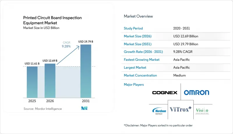
본 보고서는 검사 방법(자동 광학 검사(AOI) 등), 시스템 유형(인라인 시스템 등), 기술(2D AOI, 3D AOI 등), 최종 사용자(소비자용 전자기기 제조업체, 자동차용 전자기기 등),PCB 유형(리지드 PCB, 플렉서블 및 리지드-플렉스 PCB 등), 그리고 지역별로 분류되어 있습니다. 시장 전망은 금액(달러) 기준으로 제시되어 있습니다.
전 세계 인쇄회로기판(PCB) 검사 장비 시장 동향 및 인사이트
전자기기 분야의 소형화 진전과 부품 고밀도화
스마트폰의 부품 피치는 이미 0.3 mm까지 좁아졌으며, 각 제조업체는 수작업에 의한 육안 검사를 폐지하고, 20µm 이하의 미세 구조를 식별할 수 있는 AOI 시스템으로의 전환을 불가피하게 하고 있습니다. 50µm에서 150µm의 마이크로 비아, 블라인드 비아 및 매립 비아 스택, 재배선층 아래에 있는 구리 필러 등은 2D 그레이스케일 이미지로는 확인할 수 없습니다.
대만의 산업기술연구원(Industrial Technology Research Institute)은 2024년, 치플릿 기판의 미세한 균열을 감지할 수 있는 심자외선(DUV) 20 nm 해상도의 시제품을 시연했습니다. 5,000달러 상당의 데이터센터용 GPU 기판에서 단 하나의 결함만으로도 스크랩 비용이 발생하기 때문에 기판 1장당 15초 만에 완료되는 인라인 3D 검사는 경제적으로도 타당합니다.
자동차용 전자기기 및 전기차(EV)의 성장
세계 EV 생산 대수는 2024년에 1,400만 대에 달하고, 2030년까지 4,000만 대를 넘어설 것으로 예측됩니다. 각 EV에는 파워 모듈, 배터리 관리 보드, 운전 지원 컨트롤러가 탑재되어 있으며, 이를 합치면 내연기관 차량에 비해 PCB 사용량이 3배가 됩니다.
1차 공급업체들은 IATF 16949의 신뢰성 기준을 충족하기 위해 100% 인라인 X선 검사로 전환하고 있는 반면, ISO 26262에서는 안전 관련 어셈블리의 검사 결과에 대한 전자적 추적성이 의무화되어 있습니다. 검사의 엄격화에 따라 3D AOI 및 3D 컴퓨터 단층 촬영(CT) 플랫폼에 대한 수요가 모두 증가하고 있습니다.
고급 AOI 및 AXI 시스템에는 막대한 초기 투자가 필요합니다.
레이저 삼각측량 방식의 3D AOI 플랫폼 가격은 15만-40만 달러 범위이지만, 서브마이크론급 CT X선 시스템의 가격은 60만 달러를 초과합니다. 이러한 고비용은 특히 비용에 민감한 시장에서 사업을 전개하는 기업에게 막대한 초기 투자를 요구하기 때문에 큰 과제가 되고 있습니다. 2022년부터 2024년까지 금리 상승으로 인해 가중평균자본비용(WACC)이 150-200 베이시스 포인트 상승하면서, 투자 회수 기간이 길어지고 설비 발주가 지연됨에 따라 재무 자원에 대한 부담이 더욱 커졌습니다. 이러한 재무적 압박으로 인해 많은 기업이 자본 배분 전략을 재검토할 수밖에 없는 상황에 처해 있습니다. Equipment-as-a-Service(EaaS)는 설비 투자(CAPEX)를 운영비(OPEX)로 전환하여 기업의 초기 재무 부담을 경감시켜 주지만, 그 도입은 여전히 주로 성숙한 경제권에 국한되어 있습니다. 이러한 도입의 제한적인 확산은 해당 지역의 고도로 발달된 인프라, 유리한 규제 환경, 그리고 높은 기술적 준비도 등의 요인에 기인합니다.
부문 분석
자동 광학 검사는 2025년 매출의 56.93%를 차지하며, 2D 및 신흥 3D 광학 기술로 처리 가능한 작업의 폭이 넓음을 보여줍니다. 한편, X선 검사는 BGA(Ball Grid Array), QFN, SiP 모듈의 보급에 따라 2031년까지 연평균 성장률(CAGR) 10.74%로 확대될 것으로 예측됩니다. 컴퓨터 단층 촬영(CT) 장치는 1µm의 복셀 해상도로 마이크로 범프 및 실리콘 관통 비아(TSV) 내의 공극을 시각화하여, 파괴적인 단면 절단을 대체합니다. 0.5mm 피치를 초과하는 부품의 경우, 광학식 전용 검사 스테이션이 여전히 비용 대비 효율이 뛰어나지만, 0.3mm 피치가 주류가 됨에 따라 그 적용 범위는 좁아질 것입니다. 솔더 페이스트 검사는 스텐실 결함을 조기에 감지하기 위해 표면 실장 라인에 완벽하게 통합되어 있으며, 후공정에서의 수작업 수정 작업을 80% 이상 줄이고 있습니다.
X선 검사의 도입은 칩렛 아키텍처를 PCB 조립 현장에 도입하는 반도체 패키징 동향에 힘입고 있습니다. Comet 및 Waygate와 같은 벤더들은 현재 고처리량 기판 라인을 위해 최적화된 CT 스캐너를 제공하고 있으며, 반도체급 해상도와 컨베이어식 핸들링을 결합하고 있습니다. 광학식 검사 장비는 여전히 위험이 낮은 소비자용 제품에서 주류를 이루고 있지만, 스마트폰 분야에서도 디스플레이 하단 카메라 및 접이식 플렉서블 케이블에 대한 체적 검사가 증가하고 있습니다. 전반적으로 X선 검사 기술의 성장은 가시광선으로는 도달할 수 없는 검사 영역을 개척함으로써 인쇄회로기판(PCB) 검사 장비 시장을 주도하고 있습니다.
인라인 시스템은 2025년 수요의 60.72%를 차지하며 연평균 성장률(CAGR) 11.68%로 확대될 것으로 예측되며, 이는 모든 폼 팩터 중 가장 높은 성장률입니다. 컨베이어와의 통합을 통해 생산 흐름을 중단하지 않고, 기판 1장당 15-30초 만에 100% 검사를 수행할 수 있습니다. 프린터 및 실장기와의 폐쇄 루프 피드백을 통해 결함 감지가 즉각적인 공정 수정으로 이어지는데, 이는 오프라인 스테이션에서는 실현할 수 없는 기능입니다. 검사당 과금 계약은 검사를 소량 생산과 연동된 변동비로 취급함으로써 경제성 측면에서 인라인 시스템 도입을 더욱 촉진하고 있습니다.
오프라인 및 벤치탑형 검사 스테이션은 엔지니어링 연구소, 초기 제품 검사, 그리고 속도보다 유연성이 더 중요시되는 소량 생산 의료기기 및 항공 전자 기기 제조 현장에서 계속해서 활용되고 있습니다. 그러나 수탁 제조업체들이 여러 작업을 단일 인라인 노드로 통합함에 따라 이러한 장비의 설치 대수는 점차 감소하고 있습니다. 따라서 인쇄회로기판 검사 장비 시장은 규모 측면뿐만 아니라 스마트 팩토리 환경에서 요구되는 데이터의 상세도 측면에서도 인라인 플랫폼에 의존하는 경향을 보이고 있습니다.
지역별 분석
아시아태평양은 2025년에 전 세계 매출의 37.88%를 차지하며, 2031년까지 연평균 성장률(CAGR) 11.12%로 확대될 것으로 전망됩니다. 중국만으로도 전 세계 전자기기 제조의 28%를 차지하고 있으며, 폭스콘(Foxconn)이나 럭스쉐어 프리시전(Luxshare Precision)과 같은 수탁 조립 제조업체들이 거점을 두고 있어, 스마트폰, 노트북, 웨어러블 제품의 각 생산 라인에서 인라인 AOI를 필수로 하고 있습니다. 한국과 대만은 메모리 모듈 및 데이터센터용 가속기용 HDI 기판을 전문으로 하는 반면, 일본은 자동차 및 산업용 전자 분야에서의 프리미엄 틈새 시장을 유지하고 있어, 이는 CT 검사의 조기 도입을 정당화하고 있습니다. 중국의 ‘중국 제조 2025’나 한국의 ‘K-반도체 전략’과 같은 정부 프로그램은 스마트 팩토리용 도구에 보조금을 지급하고 있어 지역 수요를 더욱 끌어올리고 있습니다.
2025년 매출 중 북미와 유럽이 합쳐서 약 44.62%를 차지했습니다. 미국의 ‘CHIPS and Science Act’에서는 반도체 및 첨단 패키징 공장에 520억 달러가 배정되었으며, 이 중 상당 부분이 기판 및 인터포저 제조 라인용 검사 장비 도입에 사용될 예정입니다. 독일, 프랑스, 이탈리아에서는 자동차용 전자기기의 생산 능력을 확충하고 있으며, 배터리 팩 및 파워 모듈의 품질을 확보하기 위해 CT X선 검사 장비를 도입하고 있습니다. 의료기기용 FDA 21 CFR 820 및 항공우주용 AS9100과 같은 규제 체계에 따라 오프라인 CT 및 음향 현미경의 판매 기반이 확보되어 있습니다.
중동 및 아프리카, 남미는 시장 점유율이 작고 지역별로 편차가 있지만 성장세를 보이고 있습니다. 이스라엘의 방위 및 의료기기 부문에서는 IPC 클래스 3의 추적성이 필수로 요구되며, 이것이 CT 구매를 촉진하고 있습니다. 사우디아라비아와 아랍에미리트(UAE)는 경제 다각화 전략의 일환으로 국내 전자 프로그램을 출범시켜 중급 AOI 수요를 창출하고 있습니다. 브라질과 아르헨티나에서는 지역 내 소비를 위한 소비자용 전자기기 및 산업용 제어 기기가 조립되고 있으며, 비용 경쟁력이 있는 2D AOI 장비가 선호되는 한편, 인더스트리 4.0의 데이터 수집도 서서히 도입되고 있습니다. 이러한 신흥 거점들이 결합되어 인쇄회로기판 검사 장비 시장 규모를 기존의 주요 시장을 넘어 확장시키고 있습니다.
기타 혜택:
- 엑셀 형식 시장 예측(ME) 시트
- 3개월간의 애널리스트 지원
자주 묻는 질문
목차
제1장 서론
제2장 조사 방법
제3장 주요 요약
제4장 시장 구도
제5장 시장 규모와 성장 예측
제6장 경쟁 구도
제7장 시장 기회와 향후 전망
JHS 26.09.09According to Mordor Intelligence, printed circuit board inspection equipment market size in 2026 is estimated at USD 12.69 billion, growing from 2025 value of USD 11.61 billion with 2031 projections showing USD 19.79 billion, growing at 9.28% CAGR over 2026-2031.
This report is Segmented by Inspection Method (Automatic Optical Inspection, and More), System Type (Inline Systems, and More), Technology (2D AOI, 3D AOI, and More), End User (Consumer Electronics, Automotive Electronics, and More), PCB Type (Rigid PCBs, Flexible and Rigid-Flex PCBs, and More), and Geography. The Market Forecasts are Provided in Terms of Value (USD).
Global Printed Circuit Board Inspection Equipment Market Trends and Insights
Increasing Miniaturization and Higher Component Densities in Electronics
Component pitch in smartphones has already tightened to 0.3 mm, forcing manufacturers to retire manual visual checks in favour of AOI systems able to resolve features below 20 µm. Microvias between 50 µm and 150 µm, blind or buried via stacks, and copper pillars beneath redistribution layers are invisible to 2D grayscale imaging.
Taiwan's Industrial Technology Research Institute demonstrated a deep-UV 20 nm-resolution prototype in 2024 that identifies micro-cracks in chiplet substrates. As a single defect on a USD 5,000 data-center GPU substrate now drives scrap cost, inline 3D inspection at 15 s per board is economically justified.
Growth in Automotive Electronics and Electric Vehicles
Global EV output climbed to 14 million units in 2024 and is expected to surpass 40 million units by 2030. Each EV integrates power modules, battery-management boards, and driver-assistance controllers that collectively triple PCB content versus internal-combustion vehicles.
Tier-1 suppliers have moved to 100% inline X-ray inspection to meet IATF 16949 reliability standards, while ISO 26262 mandates electronic traceability of inspection results for safety-related assemblies. Increased inspection intensity lifts demand for both 3D AOI and 3D computed tomography (CT) platforms.
High Initial Capital Investments for Advanced AOI And AXI System
Prices for a laser-triangulation 3D AOI platform range from USD 150,000 to 400,000, whereas a sub-micron CT X-ray system commands a price tag exceeding USD 600,000. These high costs pose significant challenges for companies, particularly those operating in cost-sensitive markets, as they require substantial upfront investments. Between 2022 and 2024, rising interest rates pushed the weighted average cost of capital up by 150 to 200 basis points, further straining financial resources by elongating payback periods and causing delays in equipment orders. This financial pressure has led many businesses to reassess their capital allocation strategies. While equipment-as-a-service offerings transform capital expenditure into operational expenditure (OPEX), enabling companies to reduce initial financial burdens, their adoption remains largely confined to mature economies. This limited uptake is attributed to factors such as the availability of advanced infrastructure, favorable regulatory environments, and higher levels of technological readiness in these regions.
Other drivers and restraints analyzed in the detailed report include:
- Rising Adoption of Industry 4.0 Smart Manufacturing Lines
- Deployment of Advanced AI-Enabled Defect Classification Reducing False Calls
- Shortage Of Skilled Technicians for System Programming and Maintenance
For complete list of drivers and restraints, kindly check the Table Of Contents.
Segment Analysis
Automatic optical inspection delivered 56.93% of 2025 revenue, demonstrating the breadth of tasks addressable by 2D and emerging 3D optics. X-ray inspection, however, is forecast to expand at an 10.74% CAGR through 2031 as ball-grid arrays, QFNs, and SiP modules proliferate. Computed-tomography units visualize voiding in micro-bumps and through-silicon vias at 1 µm voxel resolution, replacing destructive cross-sectioning. Optical-only stations remain cost-effective for components above 0.5 mm pitch, but their addressable share will narrow as 0.3 mm pitch becomes mainstream. Solder-paste inspection is fully integrated into surface-mount lines to catch stencil defects early, reducing downstream rework by more than 80%.
X-ray adoption draws support from semiconductor packaging trends that push chiplet architectures onto PCB assembly floors. Vendors such as Comet and Waygate now offer CT scanners tailored for high-throughput board lines, merging semiconductor-class resolution with conveyorized handling. Optical stations still dominate low-risk consumer products, yet even in smartphones volumetric checks are rising for under-display cameras and folded flex tails. Overall, x-ray growth lifts the printed circuit board inspection equipment market by unlocking inspection windows unreachable by visible light.
Inline systems held 60.72% of 2025 demand and are projected to progress at a 11.68% CAGR, the fastest among all form factors. Their conveyor integration enables 100% board coverage at 15-30 s per piece without interrupting flow. Closed-loop feedback with printers and placement machines converts defect detection into immediate process correction, a capability that offline stations cannot match. Pay-per-inspection agreements further tilt economics toward inline purchases by treating inspection as a variable cost tied to low volume.
Offline and benchtop stations continue to serve engineering labs, first-article inspections, and low-volume medical, and avionics builds where flexibility outweighs speed. Yet their installed base is slowly declining as contract manufacturers consolidate multiple tasks into single inline nodes. The printed circuit board inspection equipment market therefore leans on inline platforms not only for scale but also for data granularity needed in smart-factory environments.
Complete Report Scope:
- By Inspection Method
- Automatic Optical Inspection (AOI)
- X-Ray Inspection (AXI)
- Solder Paste Inspection (SPI)
- Other Specialized Methods (Acoustic, Laser, Thermography)
- By System Type
- Inline Systems
- Offline / Benchtop Systems
- By Technology
- 2D AOI
- 3D AOI
- 2D X-Ray
- 3D / CT X-Ray
- By End User
- Consumer Electronics Manufacturers
- Automotive Electronics Manufacturers
- Industrial and Energy Electronics
- Aerospace and Defense
- Medical Device Manufacturers
- By PCB Type
- Rigid PCBs
- Flexible and Rigid-Flex PCBs
- High-Density Interconnect (HDI) PCBs
- Advanced Packaging Substrates
- Geography
- North America
- United States
- Canada
- Mexico
- Europe
- United Kingdom
- Germany
- France
- Italy
- Rest of Europe
- Asia-Pacific
- China
- Japan
- India
- South Korea
- Rest of Asia
- Middle East
- Israel
- Saudi Arabia
- United Arab Emirates
- Turkey
- Rest of Middle East
- Africa
- South Africa
- Egypt
- Rest of Africa
- South America
- Brazil
- Argentina
- Rest of South America
- North America
Geography Analysis
Asia-Pacific delivered 37.88% of global revenue in 2025 and is expected to expand at an 11.12% CAGR to 2031. China alone accounts for 28% of worldwide electronics manufacturing and hosts contract assemblers such as Foxconn and Luxshare Precision that mandate inline AOI across smartphone, laptop, and wearable lines. South Korea and Taiwan specialize in HDI substrates for memory modules and data-center accelerators, while Japan maintains a premium niche in automotive and industrial electronics that justifies early adoption of CT inspection. Government programs like China's Made in China 2025 and South Korea's K-Semiconductor Strategy subsidize smart-factory tools, further lifting regional demand.
North America and Europe jointly held roughly 44.62% of 2025 turnover. The United States CHIPS and Science Act allocate USD 52 billion for semiconductor and advanced-packaging plants, many of which will source inspection equipment for substrate and interposer lines. Germany, France, and Italy are upgrading automotive electronics capacity, installing CT X-ray to safeguard battery-pack and power-module quality. Regulatory regimes such as FDA 21 CFR 820 for medical devices and AS9100 for aerospace secure a baseline of offline CT and acoustic microscopy sales.
The Middle East, Africa, and South America contribute smaller shares but demonstrate patchy growth. Israel's defense and medical-device sector insist on IPC Class 3 traceability, prompting CT purchases. Saudi Arabia and the United Arab Emirates have launched domestic electronics programs as part of diversification agendas, adding mid-tier AOI demand. Brazil and Argentina assemble consumer electronics and industrial controls for regional consumption, favouring cost-competitive 2D AOI units yet gradually incorporating Industry 4.0 data collection. These emerging hubs collectively enlarge the printed circuit board inspection equipment market footprint beyond traditional strongholds.
- Nordson Corporation
- Koh Young Technology Inc.
- Omron Corporation
- ViTrox Corporation Berhad
- Mirtec Co., Ltd.
- Viscom AG
- Saki Corporation
- CyberOptics Corporation
- Test Research Inc.
- KLA Corporation
- Camtek Ltd.
- Yamaha Motor Co., Ltd. (Yamaha SMT)
- Unicomp Technology Co., Ltd.
- Nikon Corporation
- Comet Yxlon GmbH
- Waygate Technologies GmbH
- Shenzhen JT Automation Equipment Co., Ltd.
- GOPEL electronic GmbH
- Machine Vision Products Inc.
- Pemtron Corporation
Additional Benefits:
- The market estimate (ME) sheet in Excel format
- 3 months of analyst support
TABLE OF CONTENTS
1 INTRODUCTION
- 1.1 Study Assumptions and Market Definition
- 1.2 Scope of the Study
2 RESEARCH METHODOLOGY
3 EXECUTIVE SUMMARY
4 MARKET LANDSCAPE
- 4.1 Market Overview
- 4.2 Market Drivers
- 4.2.1 Increasing Miniaturization and Higher Component Densities in Electronics
- 4.2.2 Rising Adoption of Industry 4.0 Smart Manufacturing Lines
- 4.2.3 Growth in Automotive Electronics and Electric Vehicles
- 4.2.4 Deployment of Advanced AI-Enabled Defect Classification Reducing False Calls
- 4.2.5 Pay-Per-Inspection and Equipment-as-a-Service Business Models Lowering CapEx Barriers
- 4.2.6 Demand for Sub-Micron 3D Inspection in Advanced Packaging and Chiplet PCBs
- 4.3 Market Restraints
- 4.3.1 High Initial Capital Investments for Advanced AOI/AXI Systems
- 4.3.2 Shortage of Skilled Technicians for System Programming and Maintenance
- 4.3.3 Rapid Technology Obsolescence Leading to Compressed ROI Cycles
- 4.3.4 Radiation Safety Compliance Costs for High-Power X-Ray Inspection Lines
- 4.4 Value-Chain Analysis
- 4.5 Regulatory Landscape
- 4.6 Technological Outlook
- 4.7 Impact of Macroeconomic Factors on the Market
- 4.8 Porter's Five Forces Analysis
- 4.8.1 Threat of New Entrants
- 4.8.2 Bargaining Power of Buyers
- 4.8.3 Bargaining Power of Suppliers
- 4.8.4 Threat of Substitute Products
- 4.8.5 Intensity of Competitive Rivalry
5 MARKET SIZE AND GROWTH FORECASTS (VALUE)
- 5.1 By Inspection Method
- 5.1.1 Automatic Optical Inspection (AOI)
- 5.1.2 X-Ray Inspection (AXI)
- 5.1.3 Solder Paste Inspection (SPI)
- 5.1.4 Other Specialized Methods (Acoustic, Laser, Thermography)
- 5.2 By System Type
- 5.2.1 Inline Systems
- 5.2.2 Offline / Benchtop Systems
- 5.3 By Technology
- 5.3.1 2D AOI
- 5.3.2 3D AOI
- 5.3.3 2D X-Ray
- 5.3.4 3D / CT X-Ray
- 5.4 By End User
- 5.4.1 Consumer Electronics Manufacturers
- 5.4.2 Automotive Electronics Manufacturers
- 5.4.3 Industrial and Energy Electronics
- 5.4.4 Aerospace and Defense
- 5.4.5 Medical Device Manufacturers
- 5.5 By PCB Type
- 5.5.1 Rigid PCBs
- 5.5.2 Flexible and Rigid-Flex PCBs
- 5.5.3 High-Density Interconnect (HDI) PCBs
- 5.5.4 Advanced Packaging Substrates
- 5.6 Geography
- 5.6.1 North America
- 5.6.1.1 United States
- 5.6.1.2 Canada
- 5.6.1.3 Mexico
- 5.6.2 Europe
- 5.6.2.1 United Kingdom
- 5.6.2.2 Germany
- 5.6.2.3 France
- 5.6.2.4 Italy
- 5.6.2.5 Rest of Europe
- 5.6.3 Asia-Pacific
- 5.6.3.1 China
- 5.6.3.2 Japan
- 5.6.3.3 India
- 5.6.3.4 South Korea
- 5.6.3.5 Rest of Asia
- 5.6.4 Middle East
- 5.6.4.1 Israel
- 5.6.4.2 Saudi Arabia
- 5.6.4.3 United Arab Emirates
- 5.6.4.4 Turkey
- 5.6.4.5 Rest of Middle East
- 5.6.5 Africa
- 5.6.5.1 South Africa
- 5.6.5.2 Egypt
- 5.6.5.3 Rest of Africa
- 5.6.6 South America
- 5.6.6.1 Brazil
- 5.6.6.2 Argentina
- 5.6.6.3 Rest of South America
- 5.6.1 North America
6 COMPETITIVE LANDSCAPE
- 6.1 Market Concentration
- 6.2 Strategic Moves
- 6.3 Market Share Analysis
- 6.4 Company Profiles (includes Global Level Overview, Market Level Overview, Core Segments, Financials as available, Strategic Information, Market Rank/Share for key companies, Products and Services, and Recent Developments)
- 6.4.1 Nordson Corporation
- 6.4.2 Koh Young Technology Inc.
- 6.4.3 Omron Corporation
- 6.4.4 ViTrox Corporation Berhad
- 6.4.5 Mirtec Co., Ltd.
- 6.4.6 Viscom AG
- 6.4.7 Saki Corporation
- 6.4.8 CyberOptics Corporation
- 6.4.9 Test Research Inc.
- 6.4.10 KLA Corporation
- 6.4.11 Camtek Ltd.
- 6.4.12 Yamaha Motor Co., Ltd. (Yamaha SMT)
- 6.4.13 Unicomp Technology Co., Ltd.
- 6.4.14 Nikon Corporation
- 6.4.15 Comet Yxlon GmbH
- 6.4.16 Waygate Technologies GmbH
- 6.4.17 Shenzhen JT Automation Equipment Co., Ltd.
- 6.4.18 GOPEL electronic GmbH
- 6.4.19 Machine Vision Products Inc.
- 6.4.20 Pemtron Corporation
7 MARKET OPPORTUNITIES AND FUTURE OUTLOOK
- 7.1 White-Space and Unmet-Need Assessment