|
시장보고서
상품코드
2124976
3D IC 패키징 : 시장 점유율 분석, 업계 동향과 통계, 성장 예측(2026-2031년)3D IC Packaging - Market Share Analysis, Industry Trends & Statistics, Growth Forecasts (2026 - 2031) |
||||||
 Mordor Intelligence
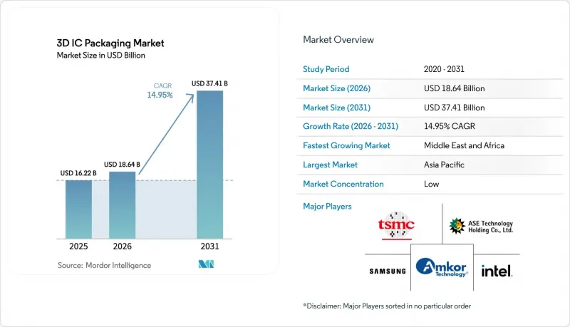
Mordor Intelligence에 의하면, 2026년 3D IC 패키징 시장 규모는 186억 4,000만 달러로 추정되며, 2025년 162억 2,000만 달러에서 2031년에는 374억 1,000만 달러에 달할 것으로 예측됩니다.
2026-2031년 연평균 성장률(CAGR)은 14.95%를 기록할 것으로 전망됩니다.
본 보고서는 패키징 기술(3D TSV, 3D WLCSP 등), 통합 기법(2.5D 인터포저,진정한 3D 스태킹 등), 디바이스 유형(메모리, 로직/프로세서 등), 최종 사용자용도(HPC 및 AI, 소비자 가전 및 모바일 등), 그리고 지역별로 분류되어 있습니다. 시장 전망은 금액(달러) 기준으로 제시되어 있습니다.
세계 3D IC 패키징 시장 동향 및 인사이트
HBM 스태킹 패키지에 대한 AI/HPC 수요의 폭발적 증가
데이터센터용 가속기의 물결이 부품표(BOM)의 우선순위를 재편하고 있으며, 3D IC 패키징 시장의 HBM 스택은 모든 첨단 노드 로드맵에서 최우선 과제가 되고 있습니다. TSMC는 Nvidia의 차세대 GPU를 지원하기 위해 2026년까지 CoWoS 생산량을월88,000 웨이퍼로 확대할 예정입니다. HBM3E에서 HBM4+로의 전환으로 인해 열 설계상의 제약을 유지한 채 유효 대역폭 밀도가 3배 증가함에 따라, 기판 제조업체들은 더 두꺼운 코어 소재나 더 미세한 구리 재분배 층의 인증을 받아야만 하는 상황에 처해 있습니다. 삼성의 H-Cube 플랫폼은 로직과 메모리를 패키지 상에서 결합하고 있으며, 이는 메모리 중심의 토폴로지가 기판 수준의 아키텍처로 확산되고 있음을 보여줍니다. 그 결과, 디바이스당 적층 다이 비율이 높아지고, TSV 구성이 더욱 다양해지며, 결국 3D IC 패키징 시장 전체에서 평균 판매 가격(ASP)이 상승하게 됩니다.
모바일 및 웨어러블 기기에서의 웨이퍼 레벨 칩 스케일 패키지(WLCSP)로의 전환
웨어러블 기기 및 프리미엄 스마트폰 제조업체들은 현재 무선 모듈, PMIC, MEMS를 7mm 미만의 플랫폼에 수용하기 위한 표준 기법으로 웨이퍼 레벨 시스템 인 패키지(WLCSP)를 채택하고 있습니다. 애플의 2026년 플래그십 모델에는 A 시리즈 SoC에 첨단 WLCSP가 채택될 것으로 널리 예상되고 있으며, 이는 폼 팩터가 기존의 ‘핀당 비용’이라는 상충 관계를 뛰어넘고 있음을 나타내는 징후입니다. 이에 대응하여 대만의 OSAT 기업들은 재배선 층 수(RDL) 우선 공정에 특화된 리소그래피 라인을 두 배로 늘려 대응하고 있는 반면, 한국의 경쟁사들은 뒤틀림을 완화하기 위해 수지 코팅된 구리박으로의 전환을 추진하고 있습니다. 이러한 움직임에 따라 3D IC 패키징 시장은 데이터센터용 실리콘의 범위를 넘어 일상적인 소비자용 디바이스로 확대되고 있으며, 이는 수익원의 다각화와 팹 가동률 향상으로 이어지고 있습니다.
TSV 제조 장비 및 CoWoS 생산 능력 부족
TSV 에칭 장비, 본딩 얼라이너, CoWoS 대응 기판 라미네이터는 여전히 12-18개월 앞까지 수주가 꽉 차 있어, AI 가속기의 납기 일정에 쫓기는 OSAT 각사의 성장 여지를 제약하고 있습니다. 애플라이드 머티리얼즈와 도쿄 일렉트론은 모두 2026년 중반까지 두 자릿수 대의 설비 수주 잔고를 예상하고 있지만, 부품 부족 및 설치 인력 부족으로 인해 실제 생산 확대는 지연되고 있습니다. TSMC가 CoWoS 기판 시장의 대부분을 차지하고 있기 때문에 구매자들은 웨이퍼 할당을 놓고 경쟁하며, 경우에 따라서는 수 분기 분량의 대금을 선불로 지불하기도 합니다. 이러한 공급 부족으로 인해, 수요 신호가 뚜렷하게 강한 경우에도 3D IC 패키징 시장 전체에서 즉각적인 수익 실현이 저해되고 있습니다.
부문별 분석
2025년, 3D TSV 노드는 3D IC 패키징 시장 점유율의 37.96%를 유지했습니다. 이는 성숙한 리소그래피 공정, 양산용 설비 및 현장 신뢰성 데이터가 메모리 공급업체의 GB당 비용 목표와 부합했기 때문입니다. 여러 HBM3E 라인에서 TSV 드릴 및 필 장비의 감가상각이 이미 완료되어, 다이 수가 증가하고 있음에도 불구하고 매출 총이익률은 안정적입니다. 한편, 하이브리드 본딩 분야는 연평균 성장률(CAGR) 21.15%로 확대되고 있으며, 구리 대 구리 직접 접촉을 활용하여 Z 방향 높이를 40%, 상호 연결 저항을 15% 줄이고 있습니다. 이러한 전기적 이점은 기존 패키지와 기판 간의 에스케이프 배선 한계를 뛰어넘는 고연산 밀도의 AI 가속기에서 매우 중요합니다.
이러한 전환으로 인해 TSV가 구식이 되는 것은 아닙니다. 오히려 두 가지 경로가 대두되고 있습니다. TSV는 대량 생산되는 메모리 및 센서 스택의 표준 기술로 남아 있는 반면, 하이브리드 본딩은 3D IC 패키징 시장에서 연산 중심이며 낮은 지연 시간이 요구되는 분야를 차지하게 될 것입니다. 인접한 제조 라인에서 두 가지 공정 모두를 처리할 수 있는 OSAT(반도체 수탁 제조업체)는 위험을 분산한 수주를 확보할 수 있습니다. 기판 제조업체들이 유리 코어의 규모 확대를 추진함에 따라 하이브리드 본딩의 정렬 정밀도는 더욱 향상되고 있으며, 이는 향후 비용 곡선이 교차하여 특정 대량 생산 SKU에서 하이브리드 본딩이 TSV를 대체하는 크로스오버 현상이 발생할 가능성을 시사합니다.
2.5D 인터포저는 실리콘 인터포저의 결함률을 0.1 dpm 미만으로 낮춘 10년에 걸친 수율 개선 성과를 바탕으로, 2025년에는 매출의 57.38%를 차지할 전망입니다. 인터포저는 프런트엔드 노드 선택과 백엔드 조립을 분리하기 때문에 GPU 벤더는 스택 전체를 재설계하지 않고도 레티클 크기의 컴퓨팅 타일을 이전 세대 노드의 I/O 다이와 함께 출하할 수 있습니다. 그러나 진정한 3D 스태킹은 연평균 성장률(CAGR) 21.28%로 성장을 지속하고, 있으며, 다이 간 지연 시간 단축을 통해 모델 학습 시간을 두 자릿수 비율로 단축할 수 있다는 점이 그 원동력이 되고 있습니다. 대표적인 이용 사례로는 수직 NAND, 메모리 인근의 컴퓨팅 렌즈, 패키지 내의 고 Q값 RF 필터 등이 있습니다. 이 모든 것은 Z축 방향의 근접성이 평면 리칫을 능가하는 시나리오입니다.
초기 신뢰성에 대한 우려-임베디드형 마이크로 범프의 전기이동이나 다이 모서리 부분의 열역학적 전단-는 낮은 탄성 계수의 언더필과 하이브리드 본딩을 통한 구리 확산 장벽으로 점차 완화되고 있습니다. 미세 유체 냉각 및 그래핀 열 확산기 기술이 성숙해짐에 따라 진정한 3D 기술의 채택이 가속화되고 있습니다. 그 결과, 3D IC 패키징 시장은 인터포저를 주류로 하는 분야와 진정한 적층 구조를 통한 고성능 분야라는 두 가지로 분화되고 있으며, 각각은 가격뿐만 아니라 차별화된 KPI 로드맵에 따라 진화를 거듭하고 있습니다.
지역별 분석
2025년, 아시아태평양은 3D IC 패키징 시장의 62.41%를 차지했습니다. 이는 대만의 첨단 노드 분야에서의 패권, 한국의 메모리 중심 백엔드 클러스터, 그리고 중국 본토의 국내 생산 능력 확대를 위한 급속한 노력에 기인합니다. TSMC의 CoWoS, 삼성의 H-Cube, ASE의 FOCoS와 같은 플랫폼이 공급업체가 밀집된 생태계를 뒷받침하고 있으며, 물류 지연을 줄이고 공정 이전 주기를 단축하고 있습니다. 그러나 지정학적 역풍 속의 이전 리스크로 인해 일부 고객은 말레이시아, 싱가포르, 베트남으로의 이중 조달을 선택할 수밖에 없게 되었으며, 이로 인해 해당 지역의 기술적 범위는 확대되는 반면, 비용 기반은 소폭 상승하고 있습니다.
북미는 최첨단 웨이퍼 및 고급 패키징 라인 모두에 대한 설비 투자를 지원하는 달러 표시 ‘CHIPS 법’에 따른 인센티브의 혜택을 받고 있습니다. TSMC의 애리조나 공장과 인텔의 오하이오 공장은 2028년까지 총월10만 장 이상의 백엔드 생산 능력을 확보할 것으로 예상되며, 이는 아시아에서 발생하는 공급 차질에 대한 완충 역할을 할 것입니다. NVIDIA, AMD 및 수많은 머신러닝 스타트업 기업들과의 지리적 근접성으로 인해 설계와 제조 간의 피드백 루프가 강화되고 있으며, 절대적인 생산량이 아시아에 미치지 못하더라도 북미는 3D IC 패키징 시장의 방향성에 있어 타의 추종을 불허하는 영향력을 가지고 있습니다.
중동 및 아프리카은 기반은 작지만 19.06%라는 가장 높은 예측 CAGR을 보이고 있습니다. UAE 정부 펀드가 지원하는 팹이나 사우디아라비아의 ‘비전 2030’ 산업 단지에서는 유리 코어 기판 라인 및 OSAT 시범 공장에 수십억 규모의 자금이 배정되고 있습니다. 유럽은 독일의 파워 일렉트로닉스 관련 전문 지식과 프랑스의 포토닉스 클러스터를 활용하여, 자동차 분야의 신뢰성과 친환경 제조 리더십에 주력하고 있습니다. 라틴아메리카는 계속해서 민수용 디바이스의 틈새 조립 거점으로 자리매김하고 있는 반면, 동유럽은 국방용 보안 패키징 구상에 주력하고 있습니다. 이러한 움직임들이 맞물리면서 생산 능력이 지리적으로 분산되고, 광범위한 3D IC 패키징 시장 내에서 지역별 수요 집적지가 형성되고 있습니다.
기타 혜택:
- 엑셀 형식 시장 예측(ME) 시트
- 3개월간의 애널리스트 지원
자주 묻는 질문
목차
제1장 A
제2장 서론
제3장 조사 방법
제4장 주요 요약
제5장 시장 구도
제6장 시장 규모 및 성장 예측(금액, 10억 달러)
제7장 경쟁 구도
제8장 시장 기회와 향후 전망
LSH 26.09.14According to Mordor Intelligence, 3D IC packaging market size in 2026 is estimated at USD 18.64 billion, growing from 2025 value of USD 16.22 billion with 2031 projections showing USD 37.41 billion, growing at 14.95% CAGR over 2026-2031.
This report is Segmented by Packaging Technology (3D TSV, 3D WLCSP and More), Integration Approach (2. 5D Interposer, True 3D Stacking, and More), Device Type (Memory, Logic/Processor and More), End-User Application (HPC & AI, Consumer Electronics & Mobile, and More), and Geography. The Market Forecasts are Provided in Terms of Value (USD).
Global 3D IC Packaging Market Trends and Insights
Explosive AI / HPC Demand for HBM-Stacked Packages
A wave of data-center accelerators is reshaping bill-of-materials priorities, pushing HBM stacks inside the 3D IC packaging market to the top of every advanced-node roadmap. TSMC is scaling CoWoS output to 88,000 wafers per month by 2026 to keep pace with Nvidia's next-generation GPUs. The shift from HBM3E to HBM4+ triples effective bandwidth density while holding thermal design limits steady, forcing substrate makers to qualify thicker core materials and finer copper redistribution layers. Samsung's H-Cube platform couples' logic and memory on-package, illustrating how memory-centric topologies are cascading down to board-level architecture. The net effect is a higher stacked-die ratio per device, a richer TSV mix and, ultimately, an elevated ASP across the 3D IC packaging market.
Mobile and Wearables Shift to Wafer-Level Chip-Scale Packages (WLCSP)
Wearable and premium-smartphone OEMs now view wafer-level system-in-package footprints as the default path to squeezing radios, PMICs and MEMS into sub-7 mm platforms. Apple's 2026 flagship is widely expected to showcase advanced WLCSP for its A-series SoC, a signal that form-factor is trumping traditional cost-per-pin trade-offs. Taiwanese OSATs have responded by doubling lithography lines dedicated to redistributed-layer-count (RDL)-first flows, while South Korean rivals pivot toward resin-coated copper foils to mitigate warpage. These moves expand the 3D IC packaging market beyond data-center silicon and into everyday consumer devices, diversifying revenue streams and improving fab loading factors.
Scarcity of Production TSV Tools and CoWoS Capacity
TSV etchers, bonding aligners and CoWoS-grade substrate laminators remain booked 12-18 months out, constraining upside for OSATs scrambling to meet AI accelerator schedules. Applied Materials and Tokyo Electron both forecast double-digit equipment backlog into mid-2026, yet component shortages and install-crew bottlenecks slow actual ramp-ups. With TSMC commanding the lion's share of CoWoS substrates, buyers compete for wafer-start allocations, sometimes pre-paying quarters in advance. The scarcity curtails immediate revenue realization across the 3D IC packaging market even when demand signals are unmistakably strong.
Other drivers and restraints analyzed in the detailed report include:
- Foundry "Foundry 2.0" Strategy Integrating Packaging
- Glass-Core and Panel-Level Substrates Lowering Cost at Scale
- Defense-Grade Chiplets Mandate Secure Heterogeneous Integration
- Thermal-Design-Limit (TDL) Challenges Beyond 1 W/mm2
For complete list of drivers and restraints, kindly check the Table Of Contents.
Segment Analysis
3D TSV nodes retained 37.96% of the 3D IC packaging market share in 2025 because mature lithographic rules, bulk production tooling and field reliability data aligned with memory vendors' cost-per-GB targets. Multiple HBM3E lines already amortized their TSV drill and fill equipment, stabilizing gross margins even as die counts increased. Yet the hybrid-bond segment is expanding at a 21.15% CAGR, levering copper-to-copper direct contact to cut z-height by 40% and interconnect resistance by 15%. These electrical gains are pivotal in compute-dense AI accelerators that push beyond traditional package-substrate escape routing limits.
The pivot does not render TSV obsolete. Instead, dual-path roadmaps emerge: TSV remains the default for high-volume memory and sensor stacks, while hybrid bonding occupies compute-centric, low-latency corners of the 3D IC packaging market. OSATs able to host both flows on adjacent lines secure risk-diversified bookings. As substrate makers scale glass cores, hy-brid bonding alignment accuracy improves further, hinting at future cross-over where cost curves intersect and hybrid bonding usurps TSV in certain volume SKUs.
2.5D interposers booked 57.38% revenue in 2025, capitalizing on a decade of yield learning that brought silicon-interposer defectivity to <0.1 dpm. Because interposers decouple front-end node choice from back-end assembly, GPU vendors ship reticle-sized compute tiles beside older-node I/O dies without redesigning the full stack. However, true 3D stacking logs a 21.28% CAGR, fuelled by die-to-die latency gains that can cut model-training time by double-digit percentages. Flagship use cases include vertical NAND, near-memory compute lenses and in-package high-Q RF filters-all scenarios where z-axis proximity beats planar reticulation.
Early reliability fears-electro-migration in buried micro-bumps and thermo-mechanical shear at die corners-are being mitigated by low-modulus under-fills and hybrid-bond copper diffusion barriers. As micro-fluidic cooling and graphene heat-spreaders mature, true 3D adoption accelerates. The 3D IC packaging market therefore bifurcates into an interposer mainstream and a true-stacked performance edge, each advancing on differentiated KPI roadmaps rather than price alone.
Complete Report Scope:
- By Packaging Technology
- 3D TSV
- 3D Wafer-Level Chip-Scale Package (WLCSP)
- Hybrid-Bond Stacking (WoW, CoW, SoIC)
- Fan-Out 3D & Panel-Level Packaging (PLP)
- By Integration Approach
- 2.5D Interposer
- True 3D Stacking
- System-in-Package / Chiplet-based HI
- By Device Type
- Memory (HBM, Wide-I/O, HMC)
- Logic / Processor
- Sensor & MEMS
- RF & Analog
- By End-User Application
- High-Performance Computing & AI
- Consumer Electronics & Mobile
- Automotive & ADAS
- Aerospace & Defence
- Medical & Industrial IoT
- Geography
- North America
- United States
- Canada
- Mexico
- Europe
- United Kingdom
- Germany
- France
- Italy
- Rest of Europe
- Asia-Pacific
- China
- Japan
- India
- South Korea
- Rest of Asia
- Middle East
- Israel
- Saudi Arabia
- United Arab Emirates
- Turkey
- Rest of Middle East
- Africa
- South Africa
- Egypt
- Rest of Africa
- South America
- Brazil
- Argentina
- Rest of South America
- North America
Geography Analysis
Asia-Pacific commanded 62.41% of the 3D IC packaging market in 2025, a consequence of Taiwan's advanced-node hegemony, South Korea's memory-centric back-end clusters and mainland China's sprint toward domestic capacity. TSMC's CoWoS, Samsung's H-Cube and ASE's FOCoS platforms anchor dense supplier habitats, driving low logistics latency and fast process transfer loops. Even so, relocation risk under geopolitical crosscurrents pushes some customers to dual source into Malaysia, Singapore and Vietnam, lengthening the region's technology reach while marginally raising cost baselines.
North America benefits from USD-denominated CHIPS Act incentives that subsidize capex for both leading-edge wafers and advanced packaging lines. TSMC Arizona and Intel Ohio collectively exceed a projected 100,000 wafers per month of back-end capacity by 2028, a cushion against Asia-bound supply disruption. Proximity to Nvidia, AMD and a host of machine-learning start-ups tightens design-manufacturing feedback loops, granting North America disproportionate influence over the direction of the 3D IC packaging market even if absolute volume lags Asia.
The Middle East and Africa region posts the highest forecast CAGR at 19.06%, albeit from a small base. Sovereign-wealth-fund-backed fabs in the UAE and Saudi Arabia's Vision 2030 industrial zones earmark billions for glass-core substrate lines and OSAT pilot plants. Europe focuses on automotive reliability and green-manufacturing leadership, leveraging German power-electronic expertise and French photonics clusters. Latin America remains a niche assembly point for consumer devices, while Eastern Europe eyes defense-oriented secure-package initiatives. Together, these moves fragment capacity geographically, opening localized demand pockets inside the broader 3D IC packaging market.
- Taiwan Semiconductor Manufacturing Co. Ltd.
- Samsung Electronics Co., Ltd.
- Advanced Semiconductor Engineering Inc.
- Amkor Technology Inc.
- Intel Corporation
- Siliconware Precision Industries Co. Ltd.
- GlobalFoundries Inc.
- Invensas Corporation
- Powertech Technology Inc.
- United Microelectronics Corporation
- Jiangsu Changjiang Electronics Technology Co. Ltd.
- Tongfu Microelectronics Co. Ltd.
- STATS ChipPAC Pte Ltd.
- ChipMOS Technologies Inc.
- ASE Test Limited
- Kyocera Corporation
- Texas Instruments Incorporated
- Micron Technology Inc.
- SK hynix Inc.
- Lam Research Corporation
Additional Benefits:
- The market estimate (ME) sheet in Excel format
- 3 months of analyst support
TABLE OF CONTENTS
1 A
2 INTRODUCTION
- 2.1 Study Assumptions & Market Definition
- 2.2 Scope of the Study
3 RESEARCH METHODOLOGY
4 EXECUTIVE SUMMARY
5 MARKET LANDSCAPE
- 5.1 Market Overview
- 5.2 Market Drivers
- 5.2.1 Explosive AI / HPC demand for HBM-stacked packages
- 5.2.2 Mobile & wearables shift to Wafer-Level Chip-Scale Packages (WLCSP)
- 5.2.3 Foundry -Foundry 2.0- strategy integrating packaging (e.g., TSMC, Samsung)
- 5.2.4 Glass-core & panel-level substrates lowering cost at scale (under-the-radar)
- 5.2.5 Defense-grade chiplets mandate secure heterogeneous integration (under-the-radar)
- 5.2.6 Carbon-neutral fabs prioritising low-temperature hybrid bonding (under-the-radar)
- 5.3 Market Restraints
- 5.3.1 Scarcity of production TSV tools & CoWoS capacity
- 5.3.2 Thermal-design-limit (TDL) challenges beyond 1 W/mm-
- 5.3.3 High IP / EDA cost for 3D floor-planning (under-the-radar)
- 5.3.4 Panel warp & yield loss >3 % in early PLP lines (under-the-radar)
- 5.4 Value / Supply-Chain Analysis
- 5.5 Regulatory Landscape
- 5.6 Technological Outlook
- 5.7 Porter-s Five Forces
- 5.7.1 Threat of New Entrants
- 5.7.2 Bargaining Power of Buyers
- 5.7.3 Bargaining Power of Suppliers
- 5.7.4 Threat of Substitutes
- 5.7.5 Competitive Rivalry
- 5.8 Pricing Analysis
6 MARKET SIZE & GROWTH FORECASTS (VALUE, USD BN)
- 6.1 By Packaging Technology
- 6.1.1 3D TSV
- 6.1.2 3D Wafer-Level Chip-Scale Package (WLCSP)
- 6.1.3 Hybrid-Bond Stacking (WoW, CoW, SoIC)
- 6.1.4 Fan-Out 3D & Panel-Level Packaging (PLP)
- 6.2 By Integration Approach
- 6.2.1 2.5D Interposer
- 6.2.2 True 3D Stacking
- 6.2.3 System-in-Package / Chiplet-based HI
- 6.3 By Device Type
- 6.3.1 Memory (HBM, Wide-I/O, HMC)
- 6.3.2 Logic / Processor
- 6.3.3 Sensor & MEMS
- 6.3.4 RF & Analog
- 6.4 By End-User Application
- 6.4.1 High-Performance Computing & AI
- 6.4.2 Consumer Electronics & Mobile
- 6.4.3 Automotive & ADAS
- 6.4.4 Aerospace & Defence
- 6.4.5 Medical & Industrial IoT
- 6.5 Geography
- 6.5.1 North America
- 6.5.1.1 United States
- 6.5.1.2 Canada
- 6.5.1.3 Mexico
- 6.5.2 Europe
- 6.5.2.1 United Kingdom
- 6.5.2.2 Germany
- 6.5.2.3 France
- 6.5.2.4 Italy
- 6.5.2.5 Rest of Europe
- 6.5.3 Asia-Pacific
- 6.5.3.1 China
- 6.5.3.2 Japan
- 6.5.3.3 India
- 6.5.3.4 South Korea
- 6.5.3.5 Rest of Asia
- 6.5.4 Middle East
- 6.5.4.1 Israel
- 6.5.4.2 Saudi Arabia
- 6.5.4.3 United Arab Emirates
- 6.5.4.4 Turkey
- 6.5.4.5 Rest of Middle East
- 6.5.5 Africa
- 6.5.5.1 South Africa
- 6.5.5.2 Egypt
- 6.5.5.3 Rest of Africa
- 6.5.6 South America
- 6.5.6.1 Brazil
- 6.5.6.2 Argentina
- 6.5.6.3 Rest of South America
- 6.5.1 North America
7 COMPETITIVE LANDSCAPE
- 7.1 Market Concentration
- 7.2 Strategic Moves
- 7.3 Market Share Analysis
- 7.4 Company Profiles (includes Global level Overview, Market level overview, Core Segments, Financials as available, Strategic Information, Market Rank/Share for key companies, Products & Services, and Recent Developments)
- 7.4.1 Taiwan Semiconductor Manufacturing Co. Ltd.
- 7.4.2 Samsung Electronics Co., Ltd.
- 7.4.3 Advanced Semiconductor Engineering Inc.
- 7.4.4 Amkor Technology Inc.
- 7.4.5 Intel Corporation
- 7.4.6 Siliconware Precision Industries Co. Ltd.
- 7.4.7 GlobalFoundries Inc.
- 7.4.8 Invensas Corporation
- 7.4.9 Powertech Technology Inc.
- 7.4.10 United Microelectronics Corporation
- 7.4.11 Jiangsu Changjiang Electronics Technology Co. Ltd.
- 7.4.12 Tongfu Microelectronics Co. Ltd.
- 7.4.13 STATS ChipPAC Pte Ltd.
- 7.4.14 ChipMOS Technologies Inc.
- 7.4.15 ASE Test Limited
- 7.4.16 Kyocera Corporation
- 7.4.17 Texas Instruments Incorporated
- 7.4.18 Micron Technology Inc.
- 7.4.19 SK hynix Inc.
- 7.4.20 Lam Research Corporation
8 MARKET OPPORTUNITIES & FUTURE OUTLOOK
- 8.1 White-Space & Unmet-Need Assessment