


|
시장보고서
상품코드
1794792
유리 기판의 혁신 : CoWoS 및 CPO 혁신 추진Glass Substrate Breakthroughs: Driving CoWoS and CPO Innovation |
||||||
유리 기판은 최근 유리관통전극(TGV) 기술의 획기적인 발전으로 첨단 반도체 패키징에서 매우 유망한 솔루션으로 부상하고 있습니다. 유리 기판은 CoWoS, CPO, FOPLP 기술 혁신을 추진할 준비가 되어 있습니다. 우수한 고주파 성능, 낮은 열팽창 계수(CTE), 우수한 치수 안정성을 활용하여 유리 기판은 I/O 밀도와 신호 무결성을 크게 향상시킵니다. 따라서 대형 인터포저, 다층 적층, 고주파 RF 애플리케이션에 특히 적합합니다. Intel, Samsung, TSMC 등 주요 기업들이 유리 기판 개발 및 채용에 적극적으로 투자하고 있는 것처럼 TGV 기술이 널리 적용되면 첨단 패키징 기술의 발전이 크게 가속화될 것입니다.
인포그래픽

주요 하이라이트
- 유리 기판은 TGV 기술의 혁신에 힘입어 첨단 반도체 패키징의 주요 신흥 재료로 부상하고 있습니다.
- 우수한 고주파 성능, 낮은 열팽창, 우수한 치수 안정성, I/O 밀도 및 신호 무결성을 향상시킵니다.
- 대형 인터포저, 다층 스태킹, 고주파 RF 시나리오에 적합합니다.
- 업계 대기업들은 유리 기판 개발에 투자하고 있으며, TGV 기술 채택과 최첨단 패키징 혁신에 박차를 가하고 있습니다.
목차
제1장 세계의 패키징 동향과 기판 재료 시장 개요
제2장 유리 기판은 비용과 성능 면에서 TSV에 도전하는 차세대 3D 통합의 물결을 주도합니다.
제3장 유리 기판은 CoWoS, CPO, FOPLP를 강화하여 새로운 시장 가능성을 열어줍니다.
제4장 TRI의 견해
KSM 25.08.27Glass substrates are emerging as a highly promising solution in advanced semiconductor packaging with recent breakthroughs in Through-Glass Via (TGV) technology. They are poised to drive innovation in CoWoS, CPO, and FOPLP technologies. Leveraging superior high-frequency performance, low coefficient of thermal expansion (CTE), and excellent dimensional stability, glass substrates significantly enhance I/O density and signal integrity. This makes them particularly well-suited for large interposers, multi-layer stacking, and high-frequency RF applications. As major players such as Intel, Samsung and TSMC actively invest in the development and adoption of glass substrates, the widespread application of TGV technology is set to profoundly accelerate the advancement of cutting-edge packaging technologies.
INFOGRAPHICS
Key Highlights:
- Glass substrates, driven by breakthroughs in TGV technology, are key emerging materials for advanced semiconductor packaging.
- They offer superior high-frequency performance, low thermal expansion, and excellent dimensional stability, boosting I/O density and signal integrity.
- Ideally suited for large interposers, multilayer stacking, and high-frequency RF scenarios.
- Major industry players are investing in glass substrate development, accelerating TGV technology adoption and cutting-edge packaging innovation.
Table of Contents
1. Global Packaging Trends and Substrate Material Market Overview
- Table 1: Materials, Technologies, and Key Specifications of FC-BGA and FC-CSP
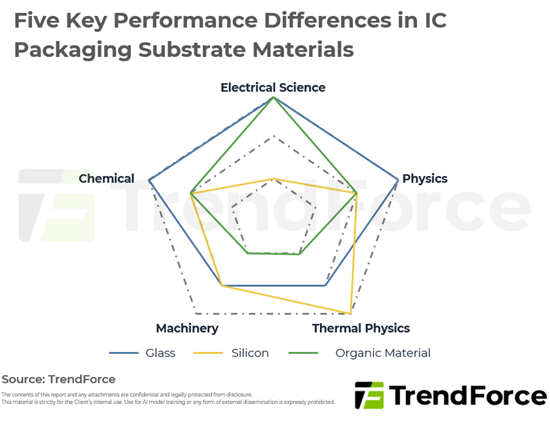
- Figure 1: Five Key Performance Differences in IC Packaging Substrate Materials
- Figure 2: Packaging Architectures Using Silicon, Organic, and Glass Materials
- Table 2: Progress of Substrate and Materials Suppliers in Glass Substrate Development (as of 1H25)
2. Glass Substrates Drive the Next Wave of 3D Integration, Challenging TSV in Cost and Performance
- Table 3: Cost-Effectiveness Comparison of TGV Fabrication Techniques
- Figure 3: Glass Substrates Can Be Applied at Scale in 2.5D/3D Packaging Types
