|
시장보고서
상품코드
2111122
GaN 기판 시장 예측(-2032년) : 기판 유형별, 웨이퍼 사이즈별, 도핑 유형별, 디바이스 유형별, 용도별, 최종 용도별, 지역별GaN Substrate Market by Substrate Type (GaN-on-Sapphire, GaN-on-Silicon, GaN-on-SiC, GaN-on-GaN, GaN-on-Diamond), Wafer Size (2-inch, 4-inch, 6-inch, 8-inch), Device Type (Discrete, ICs), Doping Type, Application, End Use - Global Forecast to 2032 |
||||||

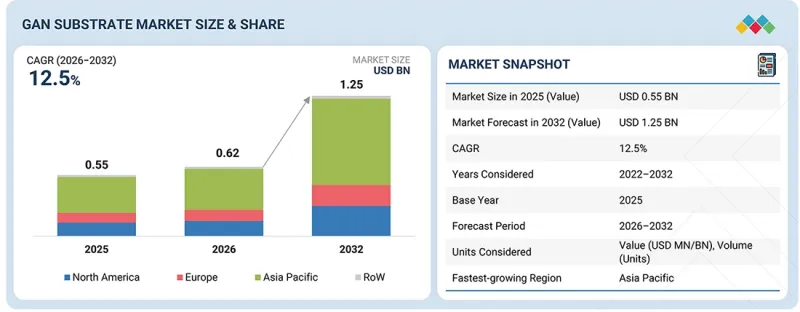
세계의 GaN 기판 시장 규모는 2026년 6억 2,000만 달러에서 2032년까지 12억 5,000만 달러로 확대하며, 예측 기간 중 CAGR은 12.5%에 달할 것으로 전망되고 있습니다.
고성능 전력 전자 및 RF 응용 분야에서 광대역 갭 반도체의 채택이 확대됨에 따라 해당 시장은 견고한 성장을 보이고 있습니다. 전기자동차, 5G 인프라, 재생 가능 에너지 시스템, 데이터센터 및 첨단 방위 기술에 대한 수요가 증가함에 따라 뛰어난 효율, 높은 전력 밀도 및 고속 스위칭 능력을 갖춘 GaN 기반 디바이스의 도입이 가속화되고 있습니다.
| 조사 범위 | |
|---|---|
| 조사 대상 기간 | 2021-2032년 |
| 기준연도 | 2025년 |
| 예측 기간 | 2026-2032년 |
| 산정 단위 | 금액(10억 달러) |
| 부문 | 기판 유형별, 웨이퍼 사이즈별, 도핑 유형별, 디바이스 유형별, 용도별, 최종 용도별, 지역별 |
| 대상 지역 | 북미, 유럽, 아시아태평양, 기타 지역 |
결정 성장 기술의 지속적인 발전, 대형 웨이퍼 생산 확대, 그리고 결함 감소로 인해 기판의 품질이 향상되는 동시에 제조 비용도 절감되고 있습니다. 주요 시장 동향으로는 국내 반도체 제조에 대한 투자, AI 및 고성능 컴퓨팅 분야에서의 GaN 채택 확대, 그리고 공급 탄력성을 강화하고 차세대 GaN 기술의 상용화를 가속화하기 위한 반도체 밸류체인 전반에 걸친 전략적 제휴 등이 있습니다.
"2026년에는 GaN-on-SiC 부문이 GaN 기판 시장에서 가장 큰 점유율을 차지할 전망"
기판 유형별로는 GaN-on-SiC 부문이 뛰어난 열전도율, 높은 절연 파괴 전압 및 탁월한 고주파 성능 덕분에 2026년에는 최대 시장 점유율을 차지할 것으로 예측됩니다. 이러한 특성 덕분에 GaN-on-SiC 기판은 통신, 항공우주·방위, 산업용 시스템 및 전기자동차에 사용되는 RF 디바이스와 고출력 전자 기기에서 최적의 선택지가 되고 있습니다. 에피택셜 성장 기술과 웨이퍼 품질의 지속적인 발전으로 인해 디바이스의 신뢰성과 제조 효율은 더욱 향상되고 있습니다. 또한 5G 인프라, 위성통신 및 고출력 애플리케이션의 도입 확대에 힘입어 예측 기간 중 GaN-on-SiC 부문의 우위는 유지될 것으로 전망됩니다.
"예측 기간 중 GaN 기판 시장에서 8인치 웨이퍼 부문이 가장 높은 연평균 성장률(CAGR)을 보일 것으로 전망됩니다."
웨이퍼 크기별로는 제조 효율 향상과 생산 비용 절감을 목적으로 한 반도체 업계의 대구경 웨이퍼 전환에 따라 예측 기간 중 8인치 웨이퍼 부문이 가장 높은 연평균 성장률(CAGR)을 기록할 것으로 전망됩니다. 소형 웨이퍼에 비해 8인치 GaN 기판은 웨이퍼당 디바이스 생산량이 많으며, 기존 반도체 제조 설비와의 호환성도 뛰어납니다. 파워 일렉트로닉스, AI 데이터센터, 자동차용 전자기기, 재생 가능 에너지 용도를 위한 대규모 GaN 제조에 대한 투자가 8인치 웨이퍼의 채택을 지원하고 있습니다. 또한 결정 성장 기술 및 웨이퍼 가공 기술의 지속적인 발전으로 전 세계에서 대구경 GaN 기판의 상업적 채택이 확대될 것으로 예상됩니다.
"2026-2032년에 GaN 기판 시장에서 가장 빠른 성장이 예상되는 지역은 아시아태평양"
아시아태평양은 반도체 제조의 급속한 확대, 전기자동차에 대한 투자 증가, 그리고 5G/6G 통신 인프라의 확대에 힘입어 예측 기간 중 가장 높은 연평균 성장률(CAGR)을 기록할 것으로 전망됩니다. 중국, 일본, 한국, 대만 등의 국가들은 첨단 소재, 웨이퍼 제조, 화합물 반도체 기술에 대한 대규모 투자를 통해 국내 반도체 생태계를 강화하고 있습니다. 또한 이 지역은 확립된 전자 부품 공급망, 강력한 정부 지원, 확대되는 연구개발(R&D) 활동의 혜택도 누리고 있습니다. 또한 GaN 기반 전력 전자, RF 소자 및 광전자 응용 분야에 대한 수요가 증가함에 따라 지역 전체에서 GaN 기판의 채택이 가속화될 것으로 예상됩니다.
GaN 기판 시장은 Sumitomo Chemical Co., Ltd.(일본)가 주도하고 있으며, 그 뒤를 Mitsubishi Chemical Corporation(일본), Shin-Etsu Chemical Co., Ltd.(일본), SOITEC(프랑스), IQE plc(영국), Wolfspeed Inc.(미국), Infineon Technologies AG(독일), Xiamen Powerway Advanced Material Co., Ltd.(중국), NGK Corporation(일본), Kyma Technologies(미국)가 뒤를 잇고 있습니다.
조사 범위
이 보고서에서는 GaN 기판 시장을 기판 유형, 웨이퍼 크기, 디바이스 유형, 도핑 유형, 용도, 최종 용도 및 지역별로 분류하고 있습니다. 또한 이 보고서에서는 시장 성장에 영향을 미치는 촉진요인, 제약 요인, 기회 및 과제에 대해서도 다루고 있습니다. 북미, 유럽, 아시아태평양, 기타 지역(RoW) 등 4대 주요 지역에 걸친 시장에 대한 상세한 분석을 제공합니다. 또한 이 보고서에는 밸류체인 분석, 경쟁 구도, 그리고 전 세계 GaN 기판 생태계에서 사업을 운영하는 주요 시장 참여 기업의 기업 개요이 포함되어 있습니다.
이 보고서 구매의 주요 이점
- 주요 촉진요인(산업용 GaN 파워 디바이스 채택 급증, 5G 및 RF 용도에서의 GaN 기판 수요 확대), 제약 요인(GaN 기판 제조에 수반되는 기술적 과제, 대체 기술과의 경쟁), 기회(탄소발자국 최소화에 대한 강력한 집중, GaN-on-silicon 기술의 발전) 및 과제(실리콘에 대한 비용 경쟁력, 복잡한 공급망 및 표준화 부재)에 대한 분석이 포함되어 있으며, 이러한 요소들이 GaN 기판 시장의 성장에 영향을 미치고 있습니다
- 제품·솔루션·서비스의 개발 및 혁신: GaN 기판 시장의 향후 제품, 연구개발 및 개발 활동에 대한 상세 인사이트
- 시장 개발: 수익성이 높은 시장에 대한 포괄적인 정보 ? 이 보고서에서는 다양한 지역의 GaN 기판 시장을 분석하고 있습니다
- 시장 다각화: 미개발 지역에서의 GaN 기판에 대한 포괄적인 정보, GaN 기판 시장의 최근 동향 및 투자 현황
- 경쟁 평가: 시장 점유율 및 성장 전략, 그리고 Sumitomo Chemical(일본), Mitsubishi Chemical Corporation(일본), Shin-Etsu Chemical(일본), IQE plc(영국), SOITEC(프랑스) 등 GaN 기판 시장의 주요 기업이 제공하는 제품 및 서비스에 대한 상세한 평가
자주 묻는 질문
목차
제1장 서론
제2장 개요
제3장 주요 인사이트
제4장 시장 개요
제5장 업계 동향
제6장 기술 진보, AI에 의한 영향, 특허, 혁신, 향후 응용
제7장 규제 상황
제8장 고객 상황과 구매 행동
제9장 GAN 기판 전도율 유형
제10장 GAN 기판 기술
제11장 GAN 기판 시장(기판 유형별)
제12장 GAN 기판 시장(웨이퍼 사이즈별)
제13장 GAN 기판 시장(도핑 유형별)
제14장 GAN 기판 시장(디바이스 유형별)
제15장 GAN 기판 시장(용도별)
제16장 GAN 기판 시장(용도별)
제17장 GAN 기판 시장(지역별)
제18장 경쟁 구도
제19장 기업 개요
제20장 조사 방법
제21장 부록
KSA 26.08.19The global GaN substrate market size is projected to grow from USD 0.62 billion in 2026 to USD 1.25 billion by 2032, at a CAGR of 12.5% during the forecast period. The market is witnessing robust growth, owing to the increasing adoption of wide-bandgap semiconductors in high-performance power electronics and RF applications. Rising demand for electric vehicles, 5G infrastructure, renewable energy systems, data centers, and advanced defense technologies is accelerating the deployment of GaN-based devices due to their superior efficiency, higher power density, and faster switching capabilities.
| Scope of the Report | |
|---|---|
| Years Considered for the Study | 2021-2032 |
| Base Year | 2025 |
| Forecast Period | 2026-2032 |
| Units Considered | Value (USD Billion) |
| Segments | By Substrate Type, Device Type and Region |
| Regions covered | North America, Europe, APAC, RoW |
Continuous advancements in crystal growth techniques, larger wafer production, and defect reduction are improving substrate quality while lowering manufacturing costs. Key market trends include investments in domestic semiconductor manufacturing, growing adoption of GaN in AI and high-performance computing applications, and strategic collaborations across the semiconductor value chain to strengthen supply resilience and accelerate commercialization of next-generation GaN technologies.
"GaN-on-SiC segment to account for the largest share of the GaN substrate market in 2026"
By substrate type, the GaN-on-SiC segment is projected to hold the largest market share in 2026 due to its superior thermal conductivity, high breakdown voltage, and excellent high-frequency performance. These characteristics make GaN-on-SiC substrates the preferred choice for RF devices and high-power electronics used in telecommunications, aerospace & defense, industrial systems, and electric vehicles. Continuous advancements in epitaxial growth technologies and wafer quality are further improving device reliability and manufacturing efficiency. Additionally, increasing deployment of 5G infrastructure, satellite communications, and high-power applications is expected to sustain the dominance of the GaN-on-SiC segment during the forecast period.
"8-inch wafer segment to exhibit the highest CAGR in the GaN substrate market during the forecast period"
By wafer size, the 8-inch wafer segment is projected to register the highest CAGR during the forecast period, owing to the semiconductor industry's transition toward larger-diameter wafers for improved manufacturing efficiency and lower production costs. Compared with smaller wafers, 8-inch GaN substrates enable higher device output per wafer and better compatibility with existing semiconductor fabrication facilities. Investments in large-scale GaN manufacturing for power electronics, AI data centers, automotive electronics, and renewable energy applications are boosting the adoption of 8-inch wafers. Furthermore, continuous advancements in crystal growth technologies and wafer processing are expected to strengthen the commercial adoption of large-diameter GaN substrates globally.
"Asia Pacific to be the fastest-growing region in the GaN substrate market between 2026 and 2032"
Asia Pacific is projected to register the highest CAGR during the forecast period due to rapid expansion of semiconductor manufacturing, increasing investments in electric vehicles, and growing deployment of 5G/6G communication infrastructure. Countries such as China, Japan, South Korea, and Taiwan are strengthening domestic semiconductor ecosystems through substantial investments in advanced materials, wafer manufacturing, and compound semiconductor technologies. The region also benefits from a well-established electronics supply chain, strong government support, and expanding R&D activities. Furthermore, the mounting demand for GaN-based power electronics, RF devices, and optoelectronic applications is expected to accelerate the adoption of GaN substrates across the region.
Breakdown of Primaries
Various executives from key organizations operating in the GaN substrate market were interviewed in-depth, including CEOs, marketing directors, and innovation and technology directors.
- By Company Type: Tier 1-40%, Tier 2-30%, and Tier 3-30%
- By Designation: Directors-20%, Managers-10%, and Others-70%
- By Region: Asia Pacific-45%, Europe-25%, North America-20%, and RoW-10%
The GaN substrate market is dominated by Sumitomo Chemical Co., Ltd. (Japan), which is followed by Mitsubishi Chemical Corporation (Japan), Shin-Etsu Chemical Co., Ltd. (Japan), SOITEC (France), IQE plc (UK), Wolfspeed Inc. (US), Infineon Technologies AG (Germany), Xiamen Powerway Advanced Material Co., Ltd. (China), NGK Corporation (Japan), and Kyma Technologies (US).
Study Coverage
The report segments the GaN substrate market by substrate type, wafer size, device type, doping type, application, end use, and region. The report also discusses the drivers, restraints, opportunities, and challenges influencing market growth. It provides a detailed view of the market across four major regions-North America, Europe, Asia Pacific, and RoW. In addition, the report includes a value chain analysis, competitive landscape, and company profiles of key market participants operating across the global GaN substrate ecosystem.
Key Benefits of Buying the Report
- Analysis of key drivers (Surging adoption of GaN power devices across industrial applications, Growing demand for GaN substrates in 5G and RF applications), restraints (Technical issues associated with GaN substrate manufacturing, Competition from alternate technologies), opportunities (Strong focus on minimizing carbon footprints, Advancements in GaN-on-silicon technology), and challenges (Cost competitiveness against silicon, Complex supply chain and lack of standardization) influencing the growth of the GaN substrate market
- Products/Solution/Service Development/Innovation: Detailed insights into upcoming products, research, and development activities in the GaN substrate market
- Market Development: Comprehensive information about lucrative markets-the report analyzes the GaN substrate market across varied regions
- Market Diversification: Exhaustive information about GaN substrate in untapped geographies, recent developments, and investments in the GaN substrate market
- Competitive Assessment: In-depth assessment of market shares and growth strategies, and offerings of leading players offering components of the GaN substrate market, such as Sumitomo Chemical Co., Ltd. (Japan), Mitsubishi Chemical Corporation (Japan), Shin-Etsu Chemical Co., Ltd. (Japan), IQE plc (UK), and SOITEC (France)
TABLE OF CONTENTS
1 INTRODUCTION
- 1.1 STUDY OBJECTIVES
- 1.2 MARKET DEFINITION
- 1.3 STUDY SCOPE
- 1.3.1 MARKETS COVERED AND REGIONAL SCOPE
- 1.3.2 INCLUSIONS AND EXCLUSIONS
- 1.3.3 YEARS CONSIDERED
- 1.4 CURRENCY CONSIDERED
- 1.5 UNIT CONSIDERED
- 1.6 LIMITATIONS
- 1.7 STAKEHOLDERS
2 EXECUTIVE SUMMARY
- 2.1 MARKET HIGHLIGHTS AND KEY INSIGHTS
- 2.2 KEY MARKET PARTICIPANTS: MAPPING OF STRATEGIC DEVELOPMENTS
- 2.3 DISRUPTIVE TRENDS IN GAN SUBSTRATE MARKET
- 2.4 HIGH-GROWTH SEGMENTS
- 2.5 REGIONAL SNAPSHOT: MARKET SIZE, GROWTH RATE, AND FORECAST
3 PREMIUM INSIGHTS
- 3.1 ATTRACTIVE OPPORTUNITIES FOR PLAYERS IN GAN SUBSTRATE MARKET
- 3.2 GAN SUBSTRATE MARKET, BY SUBSTRATE TYPE
- 3.3 GAN SUBSTRATE MARKET, BY WAFER SIZE
- 3.4 GAN SUBSTRATE MARKET, BY DOPING TYPE
- 3.5 GAN SUBSTRATE MARKET, BY DEVICE TYPE
- 3.6 GAN SUBSTRATE MARKET, BY END USE
- 3.7 GAN SUBSTRATE MARKET IN ASIA PACIFIC, BY APPLICATION AND COUNTRY
4 MARKET OVERVIEW
- 4.1 INTRODUCTION
- 4.2 MARKET DYNAMICS
- 4.2.1 DRIVERS
- 4.2.1.1 Surging adoption of GaN power devices across industrial applications
- 4.2.1.2 Growing demand for GaN substrates in 5G and RF applications
- 4.2.1.3 Rising emphasis on efficiency and compact design in electric vehicle and renewable energy sectors
- 4.2.1.4 Increasing need for high-brightness, compact, and energy-efficient LEDs
- 4.2.2 RESTRAINTS
- 4.2.2.1 Technical issues associated with GaN substrate manufacturing
- 4.2.2.2 Competition from alternative technologies
- 4.2.3 OPPORTUNITIES
- 4.2.3.1 Strong focus on minimizing carbon footprints
- 4.2.3.2 Advancements in GaN-on-silicon technology
- 4.2.3.3 Mounting GaN adoption in aerospace & defense sector
- 4.2.4 CHALLENGES
- 4.2.4.1 Cost competitiveness against silicon
- 4.2.4.2 Complex supply chain and lack of standardization
- 4.2.1 DRIVERS
- 4.3 UNMET NEEDS AND WHITE SPACES
- 4.4 INTERCONNECTED MARKETS AND CROSS-SECTOR OPPORTUNITIES
- 4.5 STRATEGIC MOVES BY TIER-1/2/3 PLAYERS
5 INDUSTRY TRENDS
- 5.1 PORTER'S FIVE FORCES ANALYSIS
- 5.1.1 THREAT OF NEW ENTRANTS
- 5.1.2 THREAT OF SUBSTITUTES
- 5.1.3 BARGAINING POWER OF SUPPLIERS
- 5.1.4 BARGAINING POWER OF BUYERS
- 5.1.5 INTENSITY OF COMPETITIVE RIVALRY
- 5.2 MACROECONOMIC OUTLOOK
- 5.2.1 INTRODUCTION
- 5.2.2 GDP TRENDS AND FORECAST
- 5.2.3 TRENDS IN GLOBAL SEMICONDUCTOR INDUSTRY
- 5.2.4 TRENDS IN GLOBAL TELECOMMUNICATIONS INDUSTRY
- 5.3 SUPPLY CHAIN ANALYSIS
- 5.4 ECOSYSTEM ANALYSIS
- 5.5 PRICING ANALYSIS
- 5.5.1 AVERAGE SELLING PRICE TREND OF GAN SUBSTRATES, BY KEY PLAYER, 2022-2025
- 5.5.2 AVERAGE SELLING PRICE TREND OF GAN SUBSTRATES, BY REGION, 2022-2025
- 5.6 TRADE ANALYSIS
- 5.6.1 IMPORT SCENARIO (HS CODE 381800)
- 5.6.2 EXPORT SCENARIO (HS CODE 381800)
- 5.7 KEY CONFERENCES AND EVENTS, 2026-2027
- 5.8 TRENDS/DISRUPTIONS IMPACTING CUSTOMER BUSINESS
- 5.9 INVESTMENT AND FUNDING SCENARIO, 2021-2025
- 5.10 CASE STUDY ANALYSIS
- 5.10.1 MITSUBISHI CHEMICAL GROUP AND JAPAN STEEL WORKS UNITE TO DEVELOP SCAAT-LP CRYSTAL GROWTH TECHNOLOGY TO BOOST GAN SUBSTRATE PRODUCTION
- 5.10.2 RICARDO PARTNERS WITH NEXPERIA TO DEVELOP HIGH-EFFICIENCY EV TRACTION INVERTER USING GAN TECHNOLOGY
- 5.10.3 SWEGAN AB DEVELOPS QUANFINE BUFFER-FREE GAN-ON-SIC EPITAXIAL TECHNOLOGY TO ADDRESS PERFORMANCE LIMITATIONS
- 5.10.4 DELTA ELECTRONICS PARTNERS WITH TEXAS INSTRUMENTS TO INTEGRATE GAN TECHNOLOGY INTO SERVER POWER SUPPLY DESIGN
- 5.10.5 CORSAIR INTEGRATES TRANSPHORM'S GAN FETS INTO NEW AX1600I PSU TO ENHANCE POWER SUPPLY
- 5.11 IMPACT OF US TARIFFS - GAN SUBSTRATE MARKET
- 5.11.1 INTRODUCTION
- 5.11.2 KEY TARIFF RATES
- 5.11.3 PRICE IMPACT ANALYSIS
- 5.11.4 IMPACT ON COUNTRIES/REGIONS
- 5.11.4.1 US
- 5.11.4.2 Europe
- 5.11.4.3 Asia Pacific
- 5.11.5 IMPACT ON END USES
6 TECHNOLOGICAL ADVANCEMENTS, AI-DRIVEN IMPACT, PATENTS, INNOVATIONS, AND FUTURE APPLICATIONS
- 6.1 KEY EMERGING TECHNOLOGIES
- 6.1.1 ADVANCED BULK GAN CRYSTAL GROWTH
- 6.1.2 LARGE-DIAMETER GAN SUBSTRATE MANUFACTURING
- 6.2 COMPLEMENTARY TECHNOLOGIES
- 6.2.1 ADVANCED EPITAXIAL GROWTH
- 6.2.2 DEFECT ENGINEERING & ADVANCED SUBSTRATE PROCESSING
- 6.3 TECHNOLOGY ROADMAP
- 6.4 PATENT ANALYSIS
- 6.5 IMPACT OF AI/GEN AI ON GAN SUBSTRATE MARKET
- 6.5.1 TOP USE CASES AND MARKET POTENTIAL
- 6.5.2 BEST PRACTICES FOLLOWED BY OEMS IN GAN SUBSTRATE MARKET
- 6.5.3 CASE STUDIES RELATED TO AI/GEN AI IMPLEMENTATION IN GAN SUBSTRATE MARKET
- 6.5.4 INTERCONNECTED ECOSYSTEM AND IMPACT ON MARKET PLAYERS
- 6.5.5 CLIENTS' READINESS TO ADOPT AI/GEN AI-INTEGRATED GAN SUBSTRATES
7 REGULATORY LANDSCAPE
- 7.1 REGULATORY LANDSCAPE
- 7.1.1 REGULATORY BODIES, GOVERNMENT AGENCIES, AND OTHER ORGANIZATIONS
- 7.1.2 STANDARDS
8 CUSTOMER LANDSCAPE AND BUYER BEHAVIOR
- 8.1 DECISION-MAKING PROCESS
- 8.2 KEY STAKEHOLDERS INVOLVED IN BUYING PROCESS AND THEIR EVALUATION CRITERIA
- 8.2.1 KEY STAKEHOLDERS IN BUYING PROCESS
- 8.2.2 BUYING CRITERIA
- 8.3 ADOPTION BARRIERS AND INTERNAL CHALLENGES
- 8.4 UNMET NEEDS OF VARIOUS END USES
- 8.5 MARKET PROFITABILITY
9 GAN SUBSTRATE CONDUCTIVITY TYPES
- 9.1 INTRODUCTION
- 9.2 SEMI-INSULATING
- 9.3 CONDUCTIVE
10 GAN SUBSTRATE TECHNOLOGIES
- 10.1 INTRODUCTION
- 10.2 METAL ORGANIC CHEMICAL VAPOR DEPOSITION (MOCVD)
- 10.3 HYDRIDE VAPOR PHASE EPITAXY (HVPE)
- 10.4 MOLECULAR BEAM EPITAXY (MBE)
11 GAN SUBSTRATE MARKET, BY SUBSTRATE TYPE
- 11.1 INTRODUCTION
- 11.2 GAN-ON-SAPPHIRE
- 11.2.1 RISING ADOPTION OF ENERGY-EFFICIENT LIGHTING SOLUTIONS AND ADVANCED DISPLAY TECHNOLOGIES TO FUEL SEGMENTAL GROWTH
- 11.3 GAN-ON-SILICON
- 11.3.1 GROWING DEMAND FOR COST-EFFECTIVE AND HIGH-PERFORMANCE POWER TO BOLSTER SEGMENTAL GROWTH
- 11.4 GAN-ON-SIC
- 11.4.1 INCREASING NEED FOR HIGH-PERFORMANCE RF DEVICES IN TELECOMMUNICATIONS AND DEFENSE SECTORS TO DRIVE MARKET
- 11.5 GAN-ON-GAN (NATIVE)
- 11.5.1 GROWING USE OF HIGH-PERFORMANCE POWER ELECTRONICS AND ADVANCED RF APPLICATIONS TO EXPEDITE SEGMENTAL GROWTH
- 11.6 GAN-ON-DIAMOND
- 11.6.1 RISING NEED FOR EXCEPTIONAL THERMAL CONDUCTIVITY AND HIGH-POWER RF TO BOLSTER SEGMENTAL GROWTH
- 11.7 FREE-STANDING GAN
- 11.7.1 INCREASING DEMAND FOR HIGH-VOLTAGE POWER DEVICES AND ADVANCED OPTOELECTRONICS TO FUEL SEGMENTAL GROWTH
- 11.8 ALGAN + GAN
- 11.8.1 RISING USAGE IN INDUSTRIAL POWER CONVERSION, DATA CENTERS, AND RENEWABLE ENERGY SYSTEMS TO SPUR DEMAND
12 GAN SUBSTRATE MARKET, BY WAFER SIZE
- 12.1 INTRODUCTION
- 12.2 2-INCH
- 12.2.1 RISING POPULARITY AMONG ACADEMIC INSTITUTIONS AND SMALL-SCALE MANUFACTURERS TO AUGMENT SEGMENTAL GROWTH
- 12.3 4-INCH
- 12.3.1 MOUNTING DEMAND FOR ADVANCED SEMICONDUCTOR TECHNOLOGIES TO CONTRIBUTE TO SEGMENTAL GROWTH
- 12.4 6-INCH
- 12.4.1 CONTINUOUS IMPROVEMENTS IN FABRICATION PROCESSES TO ACCELERATE SEGMENTAL GROWTH
- 12.5 8-INCH
- 12.5.1 GROWING FOR HIGH-PERFORMANCE SEMICONDUCTOR DEVICES TO FOSTER SEGMENTAL GROWTH
13 GAN SUBSTRATE MARKET, BY DOPING TYPE
- 13.1 INTRODUCTION
- 13.2 N-TYPE GAN
- 13.2.1 EXCELLENT ELECTRON MOBILITY, LOW ON-RESISTANCE, AND SUPERIOR ELECTRICAL PERFORMANCE TO FACILITATE SEGMENTAL GROWTH
- 13.3 P-TYPE GAN
- 13.3.1 REQUIREMENT FOR EFFICIENT LIGHT EMISSION AND RELIABLE DEVICE PERFORMANCE TO BOOST SEGMENTAL GROWTH
- 13.4 SEMI-INSULATING GAN
- 13.4.1 HIGH ELECTRICAL RESISTIVITY AND CONTROLLED IMPURITY COMPENSATION TO AUGMENT SEGMENTAL GROWTH
14 GAN SUBSTRATE MARKET, BY DEVICE TYPE
- 14.1 INTRODUCTION
- 14.2 DISCRETE
- 14.2.1 HEMT
- 14.2.1.1 High switching speeds, excellent power density, and low conduction losses to fuel segmental growth
- 14.2.2 VERTICAL GAN
- 14.2.2.1 Low defect densities and superior crystal quality to contribute to segmental growth
- 14.2.3 OTHER DISCRETE DEVICES
- 14.2.1 HEMT
- 14.3 ICS
- 14.3.1 REDUCED PARASITIC LOSSES, IMPROVED SWITCHING PERFORMANCE, AND LOWER SYSTEM-LEVEL POWER CONSUMPTION TO DRIVE MARKET
15 GAN SUBSTRATE MARKET, BY APPLICATION
- 15.1 INTRODUCTION
- 15.2 OPTOELECTRONIC DEVICES
- 15.2.1 GROWING DEMAND FOR ENERGY-EFFICIENT LIGHTING, HIGH-RESOLUTION DISPLAYS, AND UV DISINFECTION SYSTEMS TO FOSTER SEGMENTAL GROWTH
- 15.2.2 LEDS
- 15.2.2.1 UV LEDs
- 15.2.2.2 Blue LEDs
- 15.2.2.3 Green LEDs
- 15.2.2.4 White LEDs
- 15.2.3 LASERS
- 15.3 RF DEVICES
- 15.3.1 RISING NEED FOR ULTRA-FAST SIGNAL TRANSMISSION AND HIGH BANDWIDTH TO EXPEDITE SEGMENTAL GROWTH
- 15.4 POWER DEVICES
- 15.4.1 INCREASING USE OF ENERGY-EFFICIENT DEVICES IN AUTOMOTIVE AND INDUSTRIAL SECTORS TO FUEL SEGMENTAL GROWTH
16 GAN SUBSTRATE MARKET, BY END USE
- 16.1 INTRODUCTION
- 16.2 CONSUMER ELECTRONICS
- 16.2.1 MOUNTING DEMAND FOR 5G-ENABLED DEVICES AND ENERGY-EFFICIENT ELECTRONICS TO FOSTER SEGMENTAL GROWTH
- 16.3 TELECOMMUNICATIONS
- 16.3.1 EXPANDING MOBILE BROADBAND INFRASTRUCTURE AND DEMAND FOR HIGH-SPEED WIRELESS COMMUNICATION TO DRIVE MARKET
- 16.4 AUTOMOTIVE
- 16.4.1 RISING POPULARITY OF EVS AND ADVANCED DRIVER-ASSISTANCE SYSTEMS TO BOOST SEGMENTAL GROWTH
- 16.5 AEROSPACE & DEFENSE
- 16.5.1 INCREASING ADOPTION OF NEXT-GENERATION TECHNOLOGIES IN MISSION-CRITICAL APPLICATIONS TO AUGMENT SEGMENTAL GROWTH
- 16.6 ENERGY & POWER
- 16.6.1 STRONG FOCUS ON ACCELERATING SOLAR ENERGY ADOPTION AND OPTIMIZING POWER GENERATION TO EXPEDITE SEGMENTAL GROWTH
- 16.7 HEALTHCARE
- 16.7.1 RISING INTEGRATION OF GAN TECHNOLOGY IN MEDTECH APPLICATIONS TO BOOST SEGMENTAL GROWTH
- 16.8 INDUSTRIAL
- 16.8.1 GROWING EMPHASIS ON AUTOMATION AND SEMICONDUCTOR MANUFACTURING EQUIPMENT ADOPTION TO DRIVE MARKET
17 GAN SUBSTRATE MARKET, BY REGION
- 17.1 INTRODUCTION
- 17.2 NORTH AMERICA
- 17.2.1 US
- 17.2.1.1 Rapid advances in 5G infrastructure and renewable energy projects to foster market growth
- 17.2.2 CANADA
- 17.2.2.1 Growing emphasis on sustainability and electric vehicle adoption to expedite market growth
- 17.2.3 MEXICO
- 17.2.3.1 Thriving automotive industry and investments in renewable energy to contribute to market growth
- 17.2.1 US
- 17.3 EUROPE
- 17.3.1 GERMANY
- 17.3.1.1 Strong focus on electric vehicles, Industry 4.0 initiatives, 5G technology, and renewable energy to drive market
- 17.3.2 UK
- 17.3.2.1 Ambitious climate goals and push for renewable energy to expedite market growth
- 17.3.3 FRANCE
- 17.3.3.1 Strong commitment to advancing telecommunications technologies to augment market growth
- 17.3.4 NETHERLANDS
- 17.3.4.1 Rising development of semiconductor manufacturing technologies and RF devices to support market growth
- 17.3.5 ITALY
- 17.3.5.1 Growing emphasis on Industry 4.0 and smart manufacturing to accelerate market growth
- 17.3.6 SPAIN
- 17.3.6.1 Expanding renewable energy sector and telecommunications infrastructure to foster market growth
- 17.3.7 REST OF EUROPE
- 17.3.1 GERMANY
- 17.4 ASIA PACIFIC
- 17.4.1 CHINA
- 17.4.1.1 Increasing investment in 5G infrastructure, EVs, and consumer electronics to create market growth opportunities
- 17.4.2 JAPAN
- 17.4.2.1 Rapid expansion of 5G networks and semiconductor technology advancements to fuel market growth
- 17.4.3 SOUTH KOREA
- 17.4.3.1 Booming electronics and semiconductor industries to contribute to market growth
- 17.4.4 INDIA
- 17.4.4.1 Rising deployment of advanced semiconductor technologies, EVs, and renewable energy systems to bolster market growth
- 17.4.5 TAIWAN
- 17.4.5.1 Increasing investment in compound semiconductor production and government-backed innovation initiatives to drive market
- 17.4.6 SOUTHEAST ASIA
- 17.4.6.1 Expanding semiconductor manufacturing, electronics production, and advanced industrial infrastructure to fuel market growth
- 17.4.7 REST OF ASIA PACIFIC
- 17.4.1 CHINA
- 17.5 ROW
- 17.5.1 SOUTH AMERICA
- 17.5.1.1 Brazil
- 17.5.1.1.1 Expanding telecommunications infrastructure and industrial modernization to support market growth
- 17.5.1.2 Rest of South America
- 17.5.1.1 Brazil
- 17.5.2 MIDDLE EAST & AFRICA
- 17.5.2.1 GCC countries
- 17.5.2.1.1 Increasing investment in digital infrastructure, smart cities, and advanced telecommunications to augment market growth
- 17.5.2.2 South Africa
- 17.5.2.2.1 Ongoing modernization of communication networks and industrial facilities to boost market growth
- 17.5.2.3 Rest of Middle East & Africa
- 17.5.2.1 GCC countries
- 17.5.1 SOUTH AMERICA
18 COMPETITIVE LANDSCAPE
- 18.1 OVERVIEW
- 18.2 KEY PLAYER COMPETITIVE STRATEGIES/RIGHT TO WIN, 2022-2025
- 18.3 MARKET SHARE ANALYSIS, 2025
- 18.4 REVENUE ANALYSIS, 2021-2025
- 18.5 COMPANY VALUATION AND FINANCIAL METRICS
- 18.6 BRAND COMPARISON
- 18.6.1 SUMITOMO CHEMICAL CO., LTD. (JAPAN)
- 18.6.2 MITSUBISHI CHEMICAL GROUP CORPORATION (JAPAN)
- 18.6.3 SHIN-ETSU CHEMICAL CO., LTD. (JAPAN)
- 18.6.4 IQE PLC (UK)
- 18.6.5 SOITEC (FRANCE)
- 18.7 COMPANY EVALUATION MATRIX: KEY PLAYERS, 2025
- 18.7.1 STARS
- 18.7.2 EMERGING LEADERS
- 18.7.3 PERVASIVE PLAYERS
- 18.7.4 PARTICIPANTS
- 18.7.5 COMPANY FOOTPRINT, KEY PLAYERS, 2025
- 18.7.5.1 Company footprint
- 18.7.5.2 Region footprint
- 18.7.5.3 Substrate type footprint
- 18.7.5.4 Wafer size footprint
- 18.7.5.5 Application footprint
- 18.8 COMPANY EVALUATION MATRIX: STARTUPS/SMES, 2025
- 18.8.1 PROGRESSIVE COMPANIES
- 18.8.2 RESPONSIVE COMPANIES
- 18.8.3 DYNAMIC COMPANIES
- 18.8.4 STARTING BLOCKS
- 18.8.4.1 Detailed list of key startups/SMEs
- 18.8.4.2 Competitive benchmarking of key startups/SMEs
- 18.9 COMPETITIVE SCENARIO
- 18.9.1 PRODUCT LAUNCHES
- 18.9.2 DEALS
- 18.9.3 EXPANSIONS
19 COMPANY PROFILES
- 19.1 INTRODUCTION
- 19.2 KEY PLAYERS
- 19.2.1 SUMITOMO CHEMICAL CO., LTD.
- 19.2.1.1 Business overview
- 19.2.1.2 Products/Solutions/Services offered
- 19.2.1.3 Recent developments
- 19.2.1.3.1 Deals
- 19.2.1.4 MnM view
- 19.2.1.4.1 Key strengths/Right to win
- 19.2.1.4.2 Strategic choices
- 19.2.1.4.3 Weaknesses/Competitive threats
- 19.2.2 MITSUBISHI CHEMICAL GROUP CORPORATION
- 19.2.2.1 Business overview
- 19.2.2.2 Products/Solutions/Services offered
- 19.2.2.3 MnM view
- 19.2.2.3.1 Key strengths/Right to win
- 19.2.2.3.2 Strategic choices
- 19.2.2.3.3 Weaknesses/Competitive threats
- 19.2.3 SHIN-ETSU CHEMICAL CO., LTD.
- 19.2.3.1 Business overview
- 19.2.3.2 Products/Solutions/Services offered
- 19.2.3.3 Recent developments
- 19.2.3.3.1 Product launches
- 19.2.3.3.2 Deals
- 19.2.3.4 MnM view
- 19.2.3.4.1 Key strengths/Right to win
- 19.2.3.4.2 Strategic choices
- 19.2.3.4.3 Weaknesses/Competitive threats
- 19.2.4 IQE PLC
- 19.2.4.1 Business overview
- 19.2.4.2 Products/Solutions/Services offered
- 19.2.4.3 Recent developments
- 19.2.4.3.1 Product launches
- 19.2.4.3.2 Deals
- 19.2.4.4 MnM view
- 19.2.4.4.1 Key strengths/Right to win
- 19.2.4.4.2 Strategic choices
- 19.2.4.4.3 Weaknesses/Competitive threats
- 19.2.5 SOITEC
- 19.2.5.1 Business overview
- 19.2.5.2 Products/Solutions/Services offered
- 19.2.5.3 MnM view
- 19.2.5.3.1 Key strengths/Right to win
- 19.2.5.3.2 Strategic choices
- 19.2.5.3.3 Weaknesses/Competitive threats
- 19.2.6 WOLFSPEED, INC.
- 19.2.6.1 Business overview
- 19.2.6.2 Products/Solutions/Services offered
- 19.2.7 INFINEON TECHNOLOGIES AG
- 19.2.7.1 Business overview
- 19.2.7.2 Products/Solutions/Services offered
- 19.2.7.3 Recent developments
- 19.2.7.3.1 Product launches
- 19.2.7.3.2 Deals
- 19.2.8 XIAMEN POWERWAY ADVANCED MATERIAL CO., LTD.
- 19.2.8.1 Business overview
- 19.2.8.2 Products/Solutions/Services offered
- 19.2.9 NGK CORPORATION
- 19.2.9.1 Business overview
- 19.2.9.2 Products/Solutions/Services offered
- 19.2.10 KYMA TECHNOLOGIES
- 19.2.10.1 Business overview
- 19.2.10.2 Products/Solutions/Services offered
- 19.2.1 SUMITOMO CHEMICAL CO., LTD.
- 19.3 OTHER PLAYERS
- 19.3.1 IVWORKS CO., LTD.
- 19.3.2 SWEGAN
- 19.3.3 NTT ADVANCED TECHNOLOGY CORPORATION
- 19.3.4 AMERICAN ELEMENTS
- 19.3.5 SILTRONIC AG
- 19.3.6 HOMRAY MATERIAL TECHNOLOGY
- 19.3.7 ETA RESEARCH LTD.
- 19.3.8 DOWA ELECTRONICS MATERIALS CO., LTD.
- 19.3.9 SIXPOINT MATERIALS, INC.
- 19.3.10 ENKRIS SEMICONDUCTOR, INC.
- 19.3.11 AGNIT SEMICONDUCTORS PVT. LTD.
- 19.3.12 SUZHOU NANOWIN SCIENCE AND TECHNOLOGY CO., LTD.
- 19.3.13 GOETSU SEMICONDUCTOR WUXI CO., LTD.
- 19.3.14 SHANGHAI FAMOUS TRADE CO., LTD.
- 19.3.15 OMEDA INC.
20 RESEARCH METHODOLOGY
- 20.1 RESEARCH DATA
- 20.1.1 SECONDARY AND PRIMARY RESEARCH
- 20.1.2 SECONDARY DATA
- 20.1.2.1 Key data from secondary sources
- 20.1.2.2 List of key secondary sources
- 20.1.3 PRIMARY DATA
- 20.1.3.1 List of primary interview participants
- 20.1.3.2 Key data from primary sources
- 20.1.3.3 Key industry insights
- 20.1.3.4 Breakdown of primary interviews
- 20.2 MARKET SIZE ESTIMATION
- 20.2.1 BOTTOM-UP APPROACH
- 20.2.1.1 Approach to arrive at market size using bottom-up analysis
- 20.2.2 TOP-DOWN APPROACH
- 20.2.2.1 Approach to arrive at market size using top-down analysis
- 20.2.1 BOTTOM-UP APPROACH
- 20.3 DATA TRIANGULATION
- 20.4 RESEARCH ASSUMPTIONS
- 20.4.1 FORECAST-RELATED ASSUMPTIONS
- 20.5 RESEARCH LIMITATIONS
- 20.6 RISK ANALYSIS
21 APPENDIX
- 21.1 INSIGHTS FROM INDUSTRY EXPERTS
- 21.2 DISCUSSION GUIDE
- 21.3 KNOWLEDGESTORE: MARKETSANDMARKETS' SUBSCRIPTION PORTAL
- 21.4 CUSTOMIZATION OPTIONS
- 21.5 RELATED REPORTS
- 21.6 AUTHOR DETAILS