


|
시장보고서
상품코드
1550010
화학기계 연마(CMP) 패드 : 시장 점유율 분석, 산업 동향 및 통계, 성장 예측(2024-2029년)Chemical Mechanical Polishing (CMP) Pad - Market Share Analysis, Industry Trends & Statistics, Growth Forecasts (2024 - 2029) |
||||||
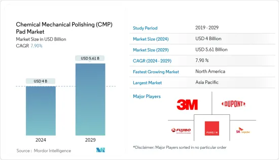
화학기계 연마(CMP) 패드 시장 규모는 2024년 40억 달러로 추정되며, 2029년에는 56억 1,000만 달러에 달할 것으로 예상되며, 예측 기간(2024-2029) 동안 CAGR 7.90%로 성장할 것으로 예상됩니다.
주요 하이라이트
- 화학기계 연마는 반도체 웨이퍼 제조 공정에서 중요한 단계입니다. 이 공정은 웨이퍼의 윗면을 연마하여 완전히 평평한 표면을 만듭니다. 이는 화학적 슬러리와 기계적 움직임을 결합하여 보다 견고하고 내구성이 뛰어난 반도체 재료를 만드는 데 필수적입니다.
- 전자기기의 성능 기준이 높아짐에 따라 반도체 및 전자기기의 소형화, 고내구성화가 요구되고 있습니다. 이에 따라 CMP와 같은 첨단 제조 재료 및 제조 기술에 대한 요구가 증가하고 있습니다. 전자 제품에 대한 수요 증가는 전자 패키징 산업을 주도하고 있으며, 고객은 새로운 전자 장비에서 향상된 기능을 기대합니다.
- 반도체 산업은 특히 반도체 제조 시 웨이퍼 연마 공정에서 화학기계 연마 패드의 중요한 수요처입니다. 자동차 전장, 스마트폰, 사물인터넷(IoT), 인공지능(AI) 기술 등의 응용 분야에 따른 반도체 수요 증가가 화학기계 연마 패드에 대한 수요를 견인하고 있습니다. 또한, 미세화 등 반도체 제조 기술의 지속적인 발전으로 인해 보다 정밀하고 효율적인 CMP 패드의 필요성이 증가하고 있습니다.
- 3DE IC, 실리콘 관통 전극(TSV), 팬아웃 웨이퍼 레벨 패키징(FOWLP)과 같은 패키징 기술의 채택이 증가함에 따라 첨단 CMP 연마 및 표면 처리 솔루션이 요구되고 있습니다. 화학적 기계 연마(CMP) 패드는 이러한 첨단 패키징 공정에서 요구되는 연마, 표면 거칠기 및 결함 수준을 달성하는 데 매우 중요합니다.
- 화학기계 연마(CMP) 패드의 재료와 제조 공정이 발전했음에도 불구하고, 여전히 기술적 한계가 존재합니다. 이러한 한계에는 매우 매끄러운 표면 달성, 표면 아래 손상 억제, 가장자리 효과 최소화, 패드 마모 및 슬러리 소비 문제 해결 등이 포함됩니다. 이러한 한계를 극복하기 위해서는 더 많은 연구 개발이 필요할 수 있으며, 이는 시장 성장을 저해하는 요인으로 작용할 수 있습니다. 또한, CMP 패드 제조업체는 공급망 중단에 따른 위험에 직면할 수 있으며, 이는 수요에 대응할 수 있는 능력에 영향을 미칠 수 있습니다.
- 기술 발전, 재료 과학의 혁신, 공정 공학의 발전과 같은 거시 경제 요인은 CMP 패드 제조업체에 도전과 기회를 제공하고 있으며, CMP 공정 제어, 결함 감소, 재료 적합성 및 표면 품질 향상과 관련된 기술적 문제를 해결하는 것이 CMP 패드 시장의 연구 개발 및 제품 혁신의 원동력이 되고 있습니다. 투자 및 제품 혁신의 원동력이 되고 있습니다. 반대로 CMP 패드의 재료, 배합 및 제조 기술의 혁신은 혁신적인 공급업체에게 경쟁 우위와 시장 기회를 창출할 수 있습니다.
화학기계 연마(CMP) 패드 시장 동향
300mm 웨이퍼 사이즈가 크게 성장할 것
- 반도체 산업에서는 첨단 제조 공정으로 인해 웨이퍼 크기가 300mm 전후로 거의 표준화되어 있습니다. 이러한 표준화는 공급망 물류를 간소화하고 반도체 제조업체, 장비 공급업체, 재료 공급업체 간의 협력을 용이하게 합니다. 그 결과, 화학적 기계적 연마(CMP) 패드 제조업체들은 업계의 수요를 충족시키기 위해 300mm 웨이퍼 가공용으로 설계된 CMP 패드 개발 및 생산에 우선순위를 두고 있습니다.
- 세계 300mm 웨이퍼 공장의 생산능력 확대 속도가 느려지고 있습니다. 그러나 업계는 여전히 견고하고 안정적인 반도체 수요에 대응하기 위해 생산능력 확대에 전념하고 있습니다. 예를 들어, 2024년 3월 인도는 반도체 제조 장비 생산을 계획하고 있으며, 어플라이드 머티어리얼즈는 벵갈루루에 검증 센터를 설립하여 선봉에 섰습니다. 또한, 300mm 웨이퍼 가공도 진행 중이며, 엔지니어링 센터를 설립하면서 생태계 구축에도 주력하고 있습니다. 이러한 기술 혁신이 조사 대상 시장의 성장을 견인하고 있습니다.
- 2023년 11월, 텍사스 인스트루먼트는 웨이퍼 주 리하이에 LFAB2라는 새로운 300mm 반도체 웨이퍼 제조 공장을 설립했으며, LFAB2의 건설은 바로 그 위치에 있는 기존 300mm 웨이퍼 공장에 연결될 예정입니다. LFAB2가 완공되면 TI의 유타 공장은 매일 수천만 개의 임베디드 및 아날로그 처리 칩을 생산할 수 있는 최대 생산능력을 갖추게 되며, LFAB2는 재생 가능한 전력으로만 운영될 예정이며, 리하이에 300mm 첨단 장비와 공정을 도입하여 폐기물, 물, 에너지 사용을 최소화할 수 있을 것입니다. 폐기물, 물, 에너지 사용량을 최소화할 수 있습니다.
- 300mm 웨이퍼 사이즈로의 전환은 종종 첨단 반도체 제조 기술의 채택 및 공정 노드 미세화(7nm 또는 5nm)와 관련이 있습니다. 이러한 첨단 노드 기술은 엄격한 성능 및 신뢰성 요구 사항을 충족하기 위해 더 엄격한 공정 제어와 향상된 연마가 필요합니다.
- 화학기계 연마(CMP) 패드는 첨단 노드 제조에 필요한 나노 스케일 수준의 평탄도를 달성하는 데 중요한 역할을 하기 때문에 수요가 높습니다.
아시아태평양이 큰 시장 점유율을 차지
- 아시아태평양은 세계 반도체 제조의 중심지이며, 중국, 대만, 한국, 일본과 같은 국가들이 반도체 제조에서 중요한 역할을 하고 있습니다. 이 지역의 반도체 제조 성장에 따라 웨이퍼 연마 공정에 사용되는 화학기계 연마(CMP) 패드에 대한 수요가 크게 증가하고 있습니다.
- 아시아태평양은 첨단 패키징 기술, 고성능 컴퓨팅, 인공지능(AI) 개발 등 기술 발전의 최전선에 있습니다. 이러한 발전에는 정밀하고 효율적인 CMP 공정이 필요하며, 이는 CMP 패드에 대한 수요를 증가시키고 있습니다.
- 이 지역에서는 새로운 반도체 제조 시설(팹)에 대한 투자와 기존 시설의 확장이 계속되고 있습니다. 공장 용량 증가와 첨단 제조 장비 도입이 CMP 패드 소비량 증가에 기여하고 있습니다. 예를 들어, 2024년 3월 Tata Electronics Private Limited(TEPL)는 대만의 Powerchip Semiconductor Manufacturing Corp.(PSMC)와 제휴하여 구자라트 주 돌레라(Dholera)에 반도체 공장을 설립했습니다. PSMC는 현재 대만에서 6개의 반도체 파운드리를 운영하고 있으며, 이 프로젝트는 9조 1,000억 인도 루피(1,097억 1,000만 달러)를 투자하고 있습니다.
- 신 팹의 생산능력은월 5만 웨이퍼로, PSMC는 전기자동차, 통신, 국방, 자동차, 가전, 디스플레이, 전력전자 등 다양한 산업을 위한 28nm 기술 기반의 고성능 컴퓨팅 칩과 전력 관리 칩 생산에 주력할 예정입니다.
- 아시아태평양은 가처분 소득 증가, 도시화, 기술 보급에 힘입어 소비자 전자제품 시장이 크게 성장하고 있습니다. 스마트폰, 노트북, 전자기기의 수요는 반도체 부품과 CMP 패드에 대한 수요를 증가시키고 있습니다.
- 또한 인도, 베트남, 인도네시아 등 아시아태평양의 신흥국에서는 다양한 분야에서 반도체 기술 채택이 증가하고 있습니다. 이들 국가는 산업화와 디지털화가 진행되고 있어 반도체 제조용 CMP 패드에 대한 수요가 크게 증가할 것으로 예상됩니다.
- 스마트 시티, 5G 네트워크, IoT 등 진행 중인 인프라 개발 프로젝트는 반도체 칩과 전자부품에 대한 수요를 촉진하고 있습니다. 화학기계 연마(CMP) 패드는 이러한 인프라 프로젝트에 필요한 첨단 반도체 소자를 생산할 수 있도록 하는 데 중요한 역할을 하고 있습니다.
- 또한, 아시아태평양의 정부와 산업계는 기술 혁신을 촉진하기 위해 반도체 연구개발에 투자하고 있습니다. 차세대 재료, 장치 및 공정 개발을 위한 연구 이니셔티브는 CMP 패드 수요에 기여하고 있습니다.
화학기계 연마(CMP) 패드 산업 개요
화학기계 연마(CMP) 패드 시장은 경쟁이 치열합니다. 대기업부터 중소기업까지 다양한 기업이 있기 때문에 매우 집중되어 있습니다. 대기업들은 모두 큰 시장 점유율을 차지하고 있으며, 세계 소비자 기반을 확대하는 데 주력하고 있습니다. 이 시장의 주요 기업으로는 3M, 듀폰, 후지방 홀딩스, 퓨리언, SK 앰펄스 등이 있습니다. 예측 기간 동안 경쟁력을 확보하기 위해 여러 기업들이 제휴, 파트너십, 인수를 통해 혁신적인 신제품을 출시하여 시장 점유율을 확대하고 있습니다.
- 2024년 4월, SK하이닉스는 한국에서 예정된 투자를 계속하기로 결정했습니다. SK하이닉스는 120조 원(7,400억 원)을 투자해 용인 반도체 클러스터에 생산 시설을 건설할 준비를 하고 있습니다. 첫 번째 공장은 2025년 3월에 착공해 2027년 초까지 완공할 예정입니다. 또한 300mm 웨이퍼 가공 장비를 사용하여 반도체 재료, 부품 및 장비를 테스트할 수 있는 미니 팹도 건설될 예정입니다.
- 2023년 9월 SK엠펄스는 반도체 기초소재 사업을 매각하고, 습식화학 사업은 국내 반도체/디스플레이 소재 기업인 야커테크놀러지에, 세정 사업은 투자회사인 선양신진에 각각 인수했습니다. 소재-부품 사업을 SK엠펄스에 통합해 화학기계 연마(CMP) 패드, 블랭크 마스크 등 반도체 전 공정 고부가 소재 사업 분야에서 존재감을 높이고 있습니다.
기타 혜택:
- 엑셀 형식의 시장 예측(ME) 시트
- 3개월간의 애널리스트 지원
목차
제1장 소개
- 조사 가정과 시장 정의
- 조사 범위
제2장 조사 방법
제3장 주요 요약
제4장 시장 인사이트
- 시장 개요
- 업계의 매력 - Porter's Five Forces 분석
- 신규 참여업체의 위협
- 구매자/소비자의 협상력
- 공급 기업의 교섭력
- 대체품의 위협
- 경쟁 기업 간의 경쟁 관계
- 기술 현황
- COVID-19의 영향과 기타 거시경제 요인이 시장에 미치는 영향
제5장 시장 역학
- 시장 성장 촉진요인
- 복잡하고 고성능인 칩/첨단 기술에 대한 요구 상승
- 소형 노드와 신아키텍처 소개
- 시장 성장 억제요인
- 반도체 산업의 주기적이고 동적인 성질
제6장 시장 세분화
- 웨이퍼 사이즈별
- 300 mm
- 200 mm
- 기타 웨이퍼 사이즈
- 지역별
- 북미
- 유럽
- 중국
- 한국
- 일본
- 대만
제7장 경쟁 상황
- 기업 개요
- 3M Co.
- DuPont de Nemours Inc.
- Fujibo Holdings Inc.
- Pureon
- SK enpulse
- Thomas West Inc.
- Hubei DingLong
- Cabot Corporation
- Entegris
- Beijing Grish Hitech Co. Ltd
제8장 투자 분석
제9장 시장 전망
ksm 24.09.13The Chemical Mechanical Polishing Pad Market size is estimated at USD 4 billion in 2024, and is expected to reach USD 5.61 billion by 2029, growing at a CAGR of 7.90% during the forecast period (2024-2029).

Key Highlights
- Chemical mechanical polishing is a crucial step in the semiconductor wafer manufacturing process. During this process, the top surface of the wafer is polished to create a completely flat surface, which is essential for building more robust and durable semiconductor materials using a combination of chemical slurry and mechanical movements.
- The rising performance standards of electronic devices are leading to a need for smaller and more durable semiconductors and electronic devices. This, in turn, increases the requirement for advanced fabrication materials and techniques such as CMP. The growing demand for electronic products drives the electronic packaging industry, with customers expecting enhanced features in new electronic devices.
- The semiconductor industry is a significant consumer of chemical mechanical polishing pads, particularly for wafer polishing processes during semiconductor manufacturing. The increasing demand for semiconductors driven by applications such as automotive electronics, smartphones, IoT devices, and AI (artificial intelligence) technologies fuels the demand for chemical mechanical polishing pads. Moreover, the continuous technological advancements in semiconductor fabrication technologies, including the development of smaller feature sizes, drive the need for more precise and efficient CMP pads.
- The rising adoption of packaging technologies such as 3DE ICs, through-silicon vias(TSVs), and fan-out wafer-level packaging (FOWLP) necessitates advanced CMP polishing and surface preparation solutions. Chemical mechanical polishing (CMP) pads are crucial in achieving the required polishing, surface roughness, and defectivity levels of these advanced packaging processes.
- Despite the advancements in chemical mechanical polishing (CMP) pad materials and manufacturing processes, certain technological limitations persist. These limitations include achieving ultra-smooth surfaces, controlling sub-surface damage, minimizing edge effects, and addressing pad wear and slurry consumption issues. Overcoming these limitations may require further research and development efforts, thus hindering the market's growth. Moreover, CMP pad manufacturers may face risks associated with supply chain disruptions, impacting the ability to meet demand.
- Macroeconomic factors such as technological advancements, material science innovations, and process engineering developments are presenting challenges and opportunities for CMP pad manufacturers. Addressing technical difficulties related to CMP process control, defect reduction, material compatibility, and surface quality improvement drives R&D investments and product innovation in the CMP pads market. Conversely, breakthroughs in CMP pad materials, formulations, or manufacturing techniques can create competitive advantages and market opportunities for innovative suppliers.
Chemical Mechanical Polishing (CMP) Pad Market Trends
300 mm Wafer Size to Witness a Significant Growth
- The semiconductor industry has largely standardized around 300 mm wafer size for advanced manufacturing processes. This standardization simplifies supply chain logistics and facilitates collaboration among semiconductor manufacturers, equipment suppliers, and materials providers. As a result, chemical mechanical polishing (CMP) pad manufacturers prioritize developing and producing CMP pads designed for 300 mm wafer processing to meet the industry demand.
- The rate of global 300 mm fab capacity expansion is slowing down. However, the industry is still dedicated to increasing capacity to keep up with the firm and consistent semiconductor demand. For instance, in March 2024, India planned to produce equipment for semiconductor manufacturing, with Applied Materials taking the lead by establishing a validation center in Bengaluru. The country is also advancing in 300 mm wafer processing and is focusing on creating a supportive ecosystem while establishing an engineering center. These innovations are driving the growth of the market studied.
- In November 2023, Texas Instruments launched a new 300 mm semiconductor wafer fabrication plant called LFAB2 in Lehi, Utah. The construction of LFAB2 will be connected to the company's existing 300 mm wafer fab in the exact location. Once LFAB2 is finished, both of TI's Utah fabs will be capable of producing tens of millions of embedded and analog processing chips daily at maximum capacity. LFAB2 aims to operate solely on renewable electricity, and the implementation of advanced 300 mm equipment and processes in Lehi will help minimize waste, water, and energy usage.
- The shift to 300 mm wafer size is often associated with adopting advanced semiconductor manufacturing technologies and smaller process nodes (7 nm and 5 nm). These advanced node technologies require tighter process control and enhanced polishing to meet stringent performance and reliability requirements.
- Chemical mechanical polishing (CMP) pads are in high demand because they play a crucial role in achieving the nanoscale-level planarity required for advanced node fabrication.
Asia-Pacific to Hold Significant Market Share
- Asia-Pacific is a global semiconductor manufacturing hub, with countries like China, Taiwan, South Korea, and Japan playing significant roles in semiconductor fabrication. The region's growth in semiconductor manufacturing drives the substantial demand for chemical mechanical polishing (CMP) pads used in wafer polishing processes.
- Asia-Pacific is at the forefront of technological advancements, including developing advanced packaging technologies, high-performance computing, and AI (artificial intelligence). These advancements require precise and efficient CMP processes, boosting the demand for CMP pads.
- The region continues to witness investments in new semiconductor fabrication facilities (fabs) and the expansion of existing ones. Increasing fab capacity and installing advanced manufacturing equipment contribute to the higher consumption of CMP pads. For instance, in March 2024, Tata Electronics Private Limited (TEPL) partnered with Taiwan's Powerchip Semiconductor Manufacturing Corp. (PSMC) to set up a semiconductor fab in Dholera, Gujarat. The investment for this project is INR 9,100 billion (USD 109.71 billion). PSMC currently operates six semiconductor foundries in Taiwan.
- The capacity of the new fabs will be 50,000 wafer starts per month. PSMC will focus on producing high-performance compute chips using 28 nm technology and power management chips for various industries such as electric vehicles, telecom, defense, automotive, consumer electronics, display, and power electronics.
- Asia-Pacific is home to a large and expanding consumer electronics market driven by rising disposable incomes, urbanization, and technological proliferation. The demand for smartphones, laptops, and electronic devices fuels the need for semiconductor components and CMP pads.
- Moreover, emerging economies in Asia-Pacific, such as India, Vietnam, and Indonesia, are witnessing increasing adoption of semiconductor technologies across various sectors. As these economies continue to industrialize and digitize, the demand for CMP pads for semiconductor manufacturing is expected to grow significantly.
- Ongoing infrastructure development projects, such as smart cities, 5G networks, and the IoT, drive demand for semiconductor chips and electronic components. The chemical mechanical polishing (CMP) pads play a significant role in enabling the production of advanced semiconductor devices required for these infrastructure projects.
- In addition, governments and industries in Asia-Pacific are investing in semiconductor R&D to foster innovation. Research initiatives aimed at developing next-generation materials, devices, and processes contribute to the demand for CMP pads.
Chemical Mechanical Polishing (CMP) Pad Industry Overview
The chemical mechanical polishing (CMP) pads market is very competitive. It is highly concentrated due to various large and small players. All the major players account for a significant market share and focus on expanding the global consumer base. Some significant players in the market are 3M Co, DuPont de Nemours Inc., Fujibo Holdings Inc., Pureon, and SK enpulse. Several companies are increasing their market share by forming collaborations, partnerships, and acquisitions and introducing new and innovative products to earn a competitive edge during the forecast period.
- In April 2024, SK Hynix was set to continue with its scheduled investments in Korea. The company is getting the Yongin Semiconductor Cluster site ready to construct production facilities, with an investment of JPY 120 trillion (USD 0.74 trillion). The first fab was expected to start construction in March 2025 and be completed by early 2027. A mini fab will also be constructed to test semiconductor materials, components, and equipment using 300 mm wafer processing equipment.
- In September 2023, SK enpulse divested its semiconductor basic materials business, with the wet chemical business purchased by the local semiconductor/display materials company Yaker Technology and the cleaning business acquired by the investment company Sunyang Shinjin. Earlier this year, SKC consolidated its semiconductor materials/parts businesses into SK enpulse to enhance its presence in high-value-added materials business areas for semiconductor front-end processes, such as chemical mechanical polishing (CMP) pads and blank masks.
Additional Benefits:
- The market estimate (ME) sheet in Excel format
- 3 months of analyst support
TABLE OF CONTENTS
1 INTRODUCTION
- 1.1 Study Assumptions and Market Definition
- 1.2 Scope of the Study
2 RESEARCH METHODOLOGY
3 EXECUTIVE SUMMARY
4 MARKET INSIGHTS
- 4.1 Market Overview
- 4.2 Industry Attractiveness - Porter's Five Forces Analysis
- 4.2.1 Threat of New Entrants
- 4.2.2 Bargaining Power of Buyers/Consumers
- 4.2.3 Bargaining Power of Suppliers
- 4.2.4 Threat of Substitute Products
- 4.2.5 Intensity of Competitive Rivalry
- 4.3 Technology Snapshot
- 4.4 Impact of COVID-19 Aftereffects and Other Macroeconomic Factors on the Market
5 MARKET DYNAMICS
- 5.1 Market Drivers
- 5.1.1 Increasing Need for Complex and High-Performance Chips/Advanced Technologies
- 5.1.2 Introduction of Smaller Nodes and New Architectures
- 5.2 Market Restraints
- 5.2.1 Cyclic and Dynamic Nature of the Semiconductor Industry
6 MARKET SEGMENTATION
- 6.1 By Wafer Size
- 6.1.1 300 mm
- 6.1.2 200 mm
- 6.1.3 Other Wafer Sizes
- 6.2 By Geography
- 6.2.1 North America
- 6.2.2 Europe
- 6.2.3 China
- 6.2.4 South Korea
- 6.2.5 Japan
- 6.2.6 Taiwan
7 COMPETITIVE LANDSCAPE
- 7.1 Company Profiles
- 7.1.1 3M Co.
- 7.1.2 DuPont de Nemours Inc.
- 7.1.3 Fujibo Holdings Inc.
- 7.1.4 Pureon
- 7.1.5 SK enpulse
- 7.1.6 Thomas West Inc.
- 7.1.7 Hubei DingLong
- 7.1.8 Cabot Corporation
- 7.1.9 Entegris
- 7.1.10 Beijing Grish Hitech Co. Ltd
