


|
시장보고서
상품코드
1630382
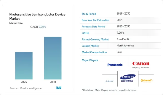
감광성 반도체 디바이스 : 시장 점유율 분석, 산업 동향 및 통계, 성장 예측(2025-2030년)Photosensitive Semiconductor Device - Market Share Analysis, Industry Trends & Statistics, Growth Forecasts (2025 - 2030) |
||||||
■ 보고서에 따라 최신 정보로 업데이트하여 보내드립니다. 배송일정은 문의해 주시기 바랍니다.
감광성 반도체 디바이스 시장은 예측 기간 동안 CAGR 9.2%를 기록할 전망입니다.
주요 하이라이트
- 포토다이오드 센서는 의료용 이미징, 분광, 펄스 옥시메트리 등의 의료기기 및 과학 기기에 폭넓게 사용되고 있어, 동 시장의 성장을 견인할 것으로 기대되고 있습니다.
- 게다가, 이미지 센서의 감광성 반도체 디바이스는 그 적용 영역을 크게 확대하고 있습니다. 예를 들어, CMOS 기술은 전자기기 제조업체가 디바이스 설계를 개선하고, 마켓플레이스에서 제품을 차별화하고, 특정 소비자 요구를 충족시키기 위해 활용하는 많은 이점을 제공합니다. 따라서 이미지 센서의 성장은 시장에서 감광성 반도체 디바이스의 성장을 뒷받침합니다.
- 중국, 인도, 한국, 대만, 일본과 같은 아시아 국가들은 이러한 장치 제조업체의 존재감이 크고 COVID-19 사이에 잠금 및 생산 일정 중단을 경험했습니다. 대부분의 세계경제가 봉쇄된 결과, 납품은 필수품에 한정되어 기업 수익 목표도 수정되었기 때문에 이 시기의 매출은 감소했습니다. 바이러스가 확산되면서 세계 각국의 정부가 가전제품 제조 공정의 폐쇄와 정지를 명했기 때문에 이 시기의 감광성 반도체 디바이스 시장은 부정적인 영향을 받았습니다. 그러나 다양한 산업, 조직, 학교, 대학에 의한 헬스케어 기기나 온라인 작업·학습의 이용은 시장의 꾸준한 성장으로 이어졌습니다.
감광성 반도체 디바이스 시장 동향
소비자용 전자기기 부문이 최대 시장 점유율을 차지할 전망
- 감광성 반도체 디바이스는 주로 많은 이미징 디바이스와 디지털 카메라에서 이미지 센서로 사용되어 이미지의 소작과 보존의 질을 향상시키고 있습니다. 이러한 이미지 용도는 산업, 미디어, 의료, 민생 용도에서 높은 채용률을 자랑합니다.
- 스마트폰, 보안 카메라, 고해상도 카메라, 캠코더에 대한 수요가 증가하고 있기 때문에 감광성 반도체 디바이스 시장은 예측 기간 동안 더욱 성장할 것으로 예상됩니다. 전 세계 제조업체들은 해상도, 성능, 픽셀 크기 등 주요 매개변수를 개선하기 위해 노력하고 있습니다.
- 게다가 CMOS 센서에서 감광성 반도체 디바이스의 사용 증가는 카메라 설계를 간소화하는 온칩에 더 많은 기능을 제공함으로써 민생 시장의 저비용 엔드에 발판을 제공합니다. 예를 들어 소니가 새로 출시한 IMX686 Exmor RS 64MP CMOS 센서는 Samsung, Huawei, OnePlus, Xiaomi 등 많은 중급형 스마트폰에 도입되고 있습니다.
- 그러나 각 업계의 기업이 경험한 상당한 경기 침체로 인해 직원의 급여도 줄어들고 있습니다. 이는 감광성 반도체 디바이스로 설계된 가전제품의 구매 결정에 직접적인 영향을 미치며 단기적으로 시장 성장에 영향을 줄 수 있습니다.
아시아태평양이 가장 급성장할 전망
- 이 지역 전체에서는 중산층에 의한 스마트폰, 태블릿, 텔레비전 등의 가전제품에 대한 지출이 증가하고 있어 가전시장의 성장을 견인해, 이 지역에서 감광성 반도체 디바이스의 성장을 이끌고 있습니다.
- 많은 기업들이 이 지역에서 신기술을 채용하여 시장을 견인할 수 있는 개발을 하고 있습니다. 예를 들어, 2022년 5월, 미쓰비시전기(Mitsubishi Electronics Co., Ltd.)는 회사가 우주공간의 진공 상태에서 위성 안테나의 3D 프린팅을 위해 감광성 수지와 태양 자외선을 사용하는 궤도상 적층 제조 기술을 개발했다고 발표했습니다.
- 또한, 2022년 1월. 도레이는 네거티브형 감광성 폴리이미드 재료를 개발했다고 발표했습니다. 이 신제품은 폴리이미드의 특징인 내열성, 기계적 특성, 접착성을 유지하면서 해상도를 높이고 100마이크로미터 및 기타 후막에 고화질 패턴 형성을 가능하게 합니다. 그리고 이것이 시장을 크게 견인하는 것 같습니다.
- 이 지역의 군대 인프라 개발에 대한 투자가 많은 것도 시장의 성장을 뒷받침하고 있습니다. 예를 들어 공식 문서와 군사 정보원에 따르면 인도는 2022-23년에 187억 6,000만 달러를 국방과 군에 지출했으며, 지역 경쟁국에 대한 전투 능력을 강화하기 위해 앞으로 더욱 증가할 것으로 예상됩니다. 이러한 투자는 감시장치 수요를 높이고, 이에 따라 이 지역의 감광성 반도체 디바이스의 성장을 뒷받침합니다.
감광성 반도체 디바이스 산업 개요
감광성 반도체 디바이스 세계 시장은 매우 세분화되어 있으며 여러 제조업체가 제품을 제공합니다. 각 회사는 더 나은 제품을 저렴한 가격으로 소비자에게 제공하기 위해 제품과 기술에 지속적으로 투자하고 있습니다. 또한 각 회사는 시장 점유율을 확대하기 위해 특히 이러한 제품을 다루는 기업을 인수합니다.
- 2022년 9월 - 후지필름 주식회사는 미러리스 디지털 카메라 「FUJIFILM X-H2」의 발매를 발표했습니다. 이 회사는 소형 경량 카메라 "X 시리즈"의 최신 라인업으로하고 있습니다. 또, 신개발의 이면 조사형 40.2MP X-Trans CMOS 5 HR센서와 고해상도의 정지화면과 고화질의 8K/30P 동영상의 촬영이 가능한 고속 X-Processor 5를 탑재하고 있다고 합니다.
- 2021년 12월 - Canon Inc.는 보안 카메라용 3.2MP SPAD 센서의 양산을 2022년에 개시한다고 발표했습니다. 이 회사에 따르면 SPAD 센서는 각 화소에 전자 소자를 탑재한 독자 설계의 이미지 센서입니다. CMOS 센서에서는 축적된 전자 전하의 판독에 전자 노이즈가 포함되어 축적광의 측정 방법에 의해 화질이 저하됩니다. 한편, SPAD 센서에서는 노이즈가 빛을 전기 신호로서 판독하는 것을 방해하지 않기 때문에 신호 노이즈가 없는 선명한 피사체의 촬영이 가능해져, 촬영시의 고감도화나 고정밀도의 측거 등의 메리트를 얻을 수 있습니다.
기타 혜택 :
- 엑셀 형식 시장 예측(ME) 시트
- 3개월간의 애널리스트 서포트
목차
제1장 서론
- 조사의 전제조건과 시장 정의
- 조사 범위
제2장 조사 방법
제3장 주요 요약
제4장 시장 역학
- 시장 개요
- 산업 밸류체인 분석
- 업계의 매력도 - Porter's Five Forces 분석
- 공급기업의 협상력
- 소비자의 협상력
- 신규 진입업자의 위협
- 대체품의 위협
- 경쟁 기업 간 경쟁 관계
- 시장 성장 촉진요인
- 이미징 및 광학 감지 솔루션 개선 수요
- 긴 수명과 저소비 전력
- 시장 성장 억제요인
- 가격 압박 증가
- COVID-19의 업계에 대한 영향 평가
제5장 시장 세분화
- 디바이스별
- 포토셀
- 포토다이오드
- 포토 트랜지스터
- 포토레지스터
- 포토IC
- 최종 사용자별
- 자동차 및 운송
- 소비자용 전자기기
- 항공우주 및 방위
- 헬스케어
- 산업
- 보안 및 보안
- 지역별
- 북미
- 유럽
- 아시아태평양
- 라틴아메리카
- 중동 및 아프리카
제6장 경쟁 구도
- 기업 프로파일
- Sony Corporation
- Samsung Electronics Co. Ltd
- Canon Inc.
- SK Hynix Inc.
- Fujifilm
- Panasonic Corporation
- Continental AG
- Robert Bosch GmbH
- Denso Corporation
- Teledyne Technologies Inc.
- Hamamatsu Photonics KK
제7장 투자 분석
제8장 시장 기회와 앞으로의 동향
KTH 25.02.05The Photosensitive Semiconductor Device Market is expected to register a CAGR of 9.2% during the forecast period.

Key Highlights
- The extensive use of photodiode sensors in medical products for medical imaging, spectroscopy, and pulse oximetry, among other medical and scientific instrumentations, is expected to drive the growth of the photodiode in the market.
- Moreover, photosensitive semiconductor devices in image sensors have immensely increased their application area. For instance, CMOS technology offers plenty of benefits that electronics manufacturers leverage to improve device design, differentiate their products in the marketplace, and meet specific consumer needs. Therefore, the growth of image sensors will boost the growth of photosensitive semiconductor devices in the market.
- Asian countries like China, India, South Korea, Taiwan, and Japan have a significant presence of manufacturers of these devices and had experience lockdowns and disrupted production schedules during Covid-19. The sales went down during that period as the lockdown in most global economies had resulted in deliveries limited to essentials and companies revising their revenue targets. Amid the spread of viruses, governments worldwide mandated the lockdown and halt of consumer electronics manufacturing processes, negatively impacting the photosensitive semiconductor device market during that period. However, the use of healthcare devices and online working and study opted by various industries, organizations, schools, and colleges led to a steady growth in the market.
Photosensitive Semiconductor Device Market Trends
Consumer Electronic Segment is Expected to Hold Largest Market Share
- Photosensitive semiconductor devices are primarily used as image sensors in many imaging devices and digital cameras to enhance the quality of cauterization and storage of images. These imaging applications have high adoption in industrial, media, medical, and consumer applications.
- Due to the increasing demand for smartphones, security cameras, high-definition cameras, and camcorders, the photosensitive semiconductor device market is expected to grow more during the forecast period. Manufacturers worldwide strive to enhance main parameters, such as resolution, performance, and pixel size.
- Additionally, the increase in the use of photosensitive semiconductor devices in CMOS sensors is providing a foothold at the low-cost end of the consumer market by offering more functions on-chip that simplify camera design. For instance, Sony's newly launched IMX686 Exmor RS 64MP CMOS sensors are being used in many mid-range phones of Samsung, Huawei, OnePlus, Xiaomi, etc.
- However, due to the vast economic downturn experienced by companies across industries, employees are also witnessing salary cuts. This may directly impact the purchase decision for consumer electronics designed with photosensitive semiconductor devices and affect the growth of the market on a short-term basis.
Asia Pacific is Expected to be the Fastest growing Region
- Across the region, there is an increase in spending by the middle class on consumer electronics products such as smartphones, tablets, televisions, etc., which is driving the consumer electronics market growth and guiding the growth of photosensitive semiconductor devices in the region.
- Many companies are using new technologies and development in the region that can drive the market. For instance, in May 2022, Mitsubishi Electric Corporation announced that the company had developed an on-orbit additive-manufacturing technology that uses photosensitive resin and solar ultraviolet light for the 3D printing of satellite antennas in the vacuum of outer space.
- Additionally, in January 2022. Toray Industries, Inc. announced that the company had developed a negative photosensitive polyimide material. This new offering maintains polyimides' characteristic thermal resistance, mechanical properties, and adhesiveness while increasing resolutions and enabling high-definition pattern formation on 100-micrometer and other thick films. And that will drive the market significantly.
- The high investments in developing the infrastructure of armed forces in the region have boosted the market's growth. For instance, according to an official document and military sources, India has spent USD 18.76 billion in the year 2022-23 on its defense and armed forces, which is expected to increase more in the future to update the armed forces and reinforce their combat capacities over regional rivals. These investments will increase the demand for surveillance equipment, which will, in turn, boost the growth of photosensitive semiconductor devices in the area.
Photosensitive Semiconductor Device Industry Overview
The Global Photosensitive Semiconductor Device Market is highly fragmented, having multiple manufacturers providing the product. Companies continuously invest in products and technology to encourage better products at lower prices for their consumers. The companies are also acquiring companies that specifically deal with these products to boost their market share.
- September 2022 - FUJIFILM Corporation announced the launch of the mirrorless digital camera 'FUJIFILM X-H2'. The company stated it as the latest addition to the X Series of compact, lightweight cameras lineup. Moreover, they also said that the camera features the new back-illuminated 40.2MP X-Trans CMOS 5 HR sensor and the high-speed X-Processor 5 capable of capturing high-resolution stills and high-definition 8K/30P video.
- December 2021 - Canon Inc. announced to start of mass production of the 3.2MP SPAD sensor for security cameras in 2022. As per the company, the SPAD sensor is a uniquely designed image sensor with each pixel possessing an electronic element. With CMOS sensors, the readout of the accumulated electronic charge contains electronic noise, which diminishes image quality due to how accumulated light is measured. Meanwhile, with SPAD sensors, noise does not interfere with the readout of light as electrical signals, which enables clear image capture of subjects free from signal noise and provides advantages such as greater sensitivity during image capture and high-precision distance measurement.
Additional Benefits:
- The market estimate (ME) sheet in Excel format
- 3 months of analyst support
TABLE OF CONTENTS
1 INTRODUCTION
- 1.1 Study Assumptions and Market Definition
- 1.2 Scope of the Study
2 RESEARCH METHODOLOGY
3 EXECUTIVE SUMMARY
4 MARKET DYNAMICS
- 4.1 Market Overview
- 4.2 Industry Value Chain Analysis
- 4.3 Industry Attractiveness - Porter's Five Forces Analysis
- 4.3.1 Bargaining Power of Suppliers
- 4.3.2 Bargaining Power of Consumers
- 4.3.3 Threat of New Entrants
- 4.3.4 Threat of Substitutes
- 4.3.5 Intensity of Competitive Rivalry
- 4.4 Market Drivers
- 4.4.1 Demand for Improved Imaging and Optical Sensing Solutions
- 4.4.2 Long Life and Low Power Consumption
- 4.5 Market Restraints
- 4.5.1 Increasing Price Pressure
- 4.6 Assessment of Impact of Covid-19 on the Industry
5 MARKET SEGMENTATION
- 5.1 Device
- 5.1.1 Photocell
- 5.1.2 Photodiode
- 5.1.3 Phototransistor
- 5.1.4 Photoresistor
- 5.1.5 Photo IC
- 5.2 End User
- 5.2.1 Automotive and Transportation
- 5.2.2 Consumer Electronics
- 5.2.3 Aerospace and Defence
- 5.2.4 Healthcare
- 5.2.5 Industrial
- 5.2.6 Security and Survelliance
- 5.3 Geography
- 5.3.1 North America
- 5.3.2 Europe
- 5.3.3 Asia Pacific
- 5.3.4 Latin America
- 5.3.5 Middle East and Africa
6 COMPETITIVE LANDSCAPE
- 6.1 Company Profiles
- 6.1.1 Sony Corporation
- 6.1.2 Samsung Electronics Co. Ltd
- 6.1.3 Canon Inc.
- 6.1.4 SK Hynix Inc.
- 6.1.5 Fujifilm
- 6.1.6 Panasonic Corporation
- 6.1.7 Continental AG
- 6.1.8 Robert Bosch GmbH
- 6.1.9 Denso Corporation
- 6.1.10 Teledyne Technologies Inc.
- 6.1.11 Hamamatsu Photonics K.K.
7 INVESTMENT ANALYSIS
8 MARKET OPPORTUNITIES AND FUTURE TRENDS


샘플 요청 목록