|
시장보고서
상품코드
1690153
EUV 리소그래피 : 시장 점유율 분석, 산업 동향, 통계, 성장 예측(2025-2030년)EUV Lithography - Market Share Analysis, Industry Trends & Statistics, Growth Forecasts (2025 - 2030) |
||||||
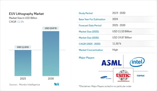
EUV 리소그래피 시장 규모는 2025년에 115억 3,000만 달러, 2030년에는 198억 7,000만 달러에 이를 것으로 예측되며, 예측 기간 중(2025년-2030년) CAGR은 11.5%를 나타낼 전망입니다.
EUV 리소그래피는 13.5nm에 불과한 파장의 빛을 사용합니다. 이것은 첨단 칩 제조의 다른 리소그래피 기술, 193nm의 빛을 사용하는 딥 울트라 바이올렛 리소그래피의 파장의 거의 14분의 1로 단축됩니다.
주요 하이라이트
- 반도체 기하학적 구조가 점점 더 작아지는 경향에 따라, 5G, AI, 자동차를 포함한 차세대 애플리케이션을 위한 최적의 효율적인 선택지를 제공하여 웨이퍼 상의 복잡한 패턴을 축소할 수 있게 해주는 EUV 리소그래피 기술의 채택이 매우 중요해졌습니다. EUV 기술에서는 EUV광의 파장이 짧기 때문에 고도의 기술에 관련하는 설계의 나노미터 스케일의 특징을 인쇄하는 것이 가능해, 칩 제조업체는 칩의 미세화를 추진할 수 있습니다.
- TSMC의 극단 자외선(EUV) 툴은 생산성숙기에 이를 전망이며, 툴의 가동률은 이미 대량생산의 목표치에 이르고 있어 일상적인 운용에서는 250와트를 넘는 출력을 얻을 수 있습니다. 7nm, 5nm, 그리고 그 이후 EUV에 기대하고 있으며, 오늘날 다른 사용 가능한 옵션은 없습니다. EUV의 사용을 원하지만,이 기술의 개발에는 아직 몇 가지 과제가 있습니다.
- TSMC 역시 2022년까지 3nm 제품의 양산을 시작할 계획입니다. SMC는 이전에 2019년 12월에 2020년 전반에 5nm 공정 기반 칩 공급을 시작하고 2022년 3nm 공정 칩의 양산을 시작한다고 발표했습니다.
- ASML은 COVID-19로 장비 수출이 어려워지고 Samsung Electronics와 TSMC 등 세계 주요 반도체 업체에 악영향을 미쳤습니다. 이에 따라 양사는 전략적인 개발 및 생산계획의 변경을 강요받고 있습니다. TSMC는 3-nm 반도체의 시험생산을 연기했습니다.
EUV 리소그래피 시장 동향
주조 제조업체가 큰 점유율을 차지할 전망
- TSMC는 2022년 3nm 제품의 양산을 시작함으로써 세계 파운드리 시장을 독점할 계획입니다. TSMC는 2019년 12월, 2020년 전반에 5nm 프로세스 기반의 칩 공급을 개시해, 2022년에 3nm 프로세스 칩의 양산을 개시한다고 발표했습니다.
- 삼성은 시장에서 일련의 과제에 직면하고 있습니다. 중국과 대만의 반도체 기업은 점점 협력관계를 깊게 하고 있습니다.
- 2021년 2월 삼성 주조는 미국에서 최첨단 반도체 제조 시설의 건설을 요구하고 애리조나, 뉴욕, 텍사스 주 당국에 서류를 제출했습니다. 1,800개의 일자리 창출이 전망되고 있습니다. 모든 것이 계획대로 진행되면, 이 파운드리는 2023년 4분기까지 가동할 예정입니다.
- 대만 세미컨덕터 매뉴팩처링사(TSMC)나 유나이티드 마이크로 일렉트로닉스사(UMC) 등 벤더들은 폭스바겐과 도요타 등 자동차 제조업체 수요에 부응하기 위해 생산 이전에 주력하고 있다고 발표했습니다. 또한 Qualcomm 및 Apple과 같은 기업 수요가 반도체 공급에 뒤처져 있습니다. 오토모티브 뉴스의 새로운 조사(2021년 4월)에 따르면 응답자의 53%가 칩을 미국외에서 조달하고 있음을 시사하고, 제조업체의 55%가 국외에서 대체 칩 조달처를 찾고 있습니다.
- 이러한 요인이 조사 대상 시장에 신규 기업의 진입으로 이어지고 있습니다. 예를 들어, 인텔은 최근 자동차 제조업체 수요에 대응하기 위해 새로운 비즈니스 인텔 주조 서비스의 출시를 발표했습니다. 마찬가지로 2021년 3월 세계 주조는 포드, 폭스바겐, 제너럴 모터스 등 자동차 제조업체의 감산을 지원하기 위해 세계 각지에서 생산 능력 확장을 위해 14억 달러를 투자할 예정이라고 발표했습니다.
아시아태평양이 큰 점유율을 차지할 전망
- 극단 자외선(EUV) 리소그래피 세계 시장에서 아시아태평양은 계속해서 가장 큰 판매 점유율을 차지합니다. 예측 기간 동안 이 지역에서는 대만이 우위를 차지할 것으로 예상됩니다. 대만의 TSMC 사업 확대와 EUV 리소그래피 기술 투자 증가는 대만의 극단적 자외선 리소그래피 시장 성장을 지원하는 가장 중요한 요소 중 하나입니다. 대만은 아시아태평양 EUV 리소그래피 시장의 대부분의 수익 점유율을 차지합니다. 대만 이외에서는 일본, 중국, 한국의 극단 자외선 리소그래피 시장이 앞으로 수년간 이해관계자들에게 큰 기회를 가져올 것으로 기대되고 있습니다.
- 미국과 중국의 무역마찰이 격화되는 가운데, 중국의 반도체 제조업체도 자국 제품의 생산을 서두르기 위해, 중고의 칩 제조 장치를 활용하고 있어 일본의 중고 시장에서의 장비 가격을 끌어 올리고 있습니다.
- 코로나바이러스 팬데믹으로 인한 재택근무 트렌드도 한 요인입니다.
- ASML의 새로운 교육 시설은 아마도 두 회사 모두에게 유익하다고 생각할 것입니다. Review에 따르면 ASML이 올해 출하 예정인 35대의 EUV 시스템 중 20대가 TSMC용이라고 합니다. 르를 다루는 것으로, 장래의 판매를 준비하고 있습니다.
EUV 리소그래피 산업 개요
EUV 리소그래피 시장은 ASML이 극단적인 자외선을 사용하는 리소그래피 장비의 유일한 제조업체이기 때문에 고도로 통합되어 있습니다.인텔, 삼성, 대만 TSMC(Taiwan Semiconductor Manufacturing Company)를 포함한 일부 글로벌 반도체 제조사(파운드리)에 자사 장비를 제조하여 판매합니다. 이 회사의 기업 수익의 거의 25%는 EUV 노광 장치의 판매에 의한 것으로, 이것은 EUV 노광 장치의 제조와 상업화에 있어서의 회사의 독점을 반영하고 있습니다.
- 2021년 12월 유럽에서 인기있는 ASML은 극단 자외선 리소그래피 장치의 개발을 위해 노력하고 있습니다.
- 2021년 3월 삼성은 세계 최대의 주조공장인 TSMC에 대항하기 위해 EUV 스캐너를 생산하고 있습니다.
기타 혜택 :
- 엑셀 형식 시장 예측(ME) 시트
- 3개월간의 애널리스트 지원
목차
제1장 서론
- 조사의 전제조건과 시장 정의
- 조사 범위
제2장 조사 방법
제3장 주요 요약
제4장 시장 인사이트
- 시장 개요
- 산업 밸류체인 분석
- 업계의 매력도 - Porter's Five Forces 분석
- 공급기업의 협상력
- 구매자의 협상력
- 신규 참가업체의 위협
- 대체품의 위협
- 경쟁 기업간 경쟁 관계의 강도
- COVID-19의 업계에 대한 영향 평가
제5장 시장 역학
- 시장 성장 촉진요인
- 다른 것에 비해 마이크로칩의 생산 속도가 빨라지는 기술
- 칩 제조업체에 의한 효율 향상을 위한 제조 공정 삭감
- 시장 성장 억제요인
- 기존 Deep UV 레이저에서 EUV 레이저로의 교체에 따른 고비용
- 시장내의 독점
- 기술 스냅샷
제6장 시장 세분화
- 제품 유형
- 광원
- 미러
- 마스크
- 유형
- 주조
- 집적 디바이스 제조업체(IDM)
- 지역
- 한국
- 대만
- 기타
제7장 경쟁 구도
- 기업 프로파일
- ASML Holding NV
- NTT Advanced Technology Corporation
- Canon Inc.
- Nikon Corporation
- Intel Corporation
- Taiwan Semiconductor Manufacturing Company Limited
- Samsung Electronics Co. Ltd
- Toppan Photomasks Inc.
- Ushio, Inc.
제8장 투자 분석
제9장 시장의 미래
SHW 25.05.09The EUV Lithography Market size is estimated at USD 11.53 billion in 2025, and is expected to reach USD 19.87 billion by 2030, at a CAGR of 11.5% during the forecast period (2025-2030).

EUV lithography makes the usage of light with a wavelength of just 13.5 nm, which is a reduction of almost 14 times the wavelength of the other lithography techniques in advanced chipmaking, Deep Ultraviolet lithography, which uses 193 nm light. ASML, which is the dominant player in the market, has been exploring ways to reduce transistor sizes and has made considerable strides in the field of EUV lithography, which enables more precise and efficient production of semiconductors at small transistor scales around 7nm node size or even 5nm.
Key Highlights
- As semiconductor geometries tend to grow smaller and smaller, the adoption of EUV lithography technology has become extremely important, as it enables scaling down of intricate patterns on wafers by providing an optimal and efficient choice for next-generation applications, including 5G, AI, and Automotive. EUV technology allows the chip makers to keep driving chip scaling as the shorter wavelength of EUV light is capable of printing the nanometer-scale features of the designs related to the advanced techniques.
- TSMC's Extreme Ultraviolet (EUV) tools are expected to reach production maturity, with tool availability already reaching target goals for high-volume production and output power of greater than 250 watts for daily operations. Chipmakers are banking on EUV at 7nm, 5nm, and beyond for leading-edge logic, and today there are no other options available. The next-generation lithography technologies are not ready and can not be applied at 7nm and 5nm scales. At 3nm and beyond, chipmakers hope to use high-NA EUV, but several challenges have yet to be overcome in developing this technology.
- TSMC has also been planning to start the volume production of the 3-nm products by 2022. Samsung Electronics Co. Ltd, another major player in the market, aims to overtake TSMC by 2030 with its extreme ultraviolet (EUV) lithography technology. TSMC, previously in Dec 2019, announced that the company would be starting to supply 5 Nm process-based chips in the first half of 2020 and will be starting mass production of 3-nm process chips in 2022. The company also anticipates producing 2-nm process products by 2024.
- ASML faced difficulty exporting its equipment due to COVID-19, negatively affecting major global semiconductor producers, including Samsung Electronics and TSMC. A delay in the company's equipment delivery is forcing the two companies to change their strategic development and production roadmaps. Due to a delay in the delivery of the company's equipment, the two companies have to alter their strategic development and production plans. TSMC has postponed the test production of 3-nm semiconductors. Samsung Electronics, meantime, had hoped to commence commercial production of 5-nm semiconductors in 2020 but was unable to do so until late 2021.
EUV Lithography Market Trends
Foundry is Expected to Hold Major Share
- TSMC is planning to dominate the global foundry market by starting the volume production of 3-nm products in 2022. Samsung Electronics Co, Ltd, the runner-up in the market, is aiming to overtake TSMC in 2030 with its extreme ultraviolet (EUV) lithography technology. TSMC announced in December 2019 that the company would start to supply 5-nm process-based chips in the first half of 2020 and start the mass production of 3-nm process chips in 2022. The company also expects o produce 2-nm process products in 2024.
- Samsung is facing a series of challenges in the market. For instance, the supply of photoresists for EUV lithography purposes can be subject to Japan's export restrictions. Besides, a significant number of companies are trying to compete with Samsung Electronics. Chinese and Taiwanese semiconductor companies are increasingly collaborating. Samsung Electronics has unveiled a series of new microfabrication techniques such as FinFET, gate-all-around, and multi-bridge-channel FET to compete with the increasing competitors.
- In February 2021, Samsung Foundry filed documents with authorities in Arizona, New York, and Texas seeking to build a leading-edge semiconductor manufacturing facility in the United States. The potential fab near Austin, Texas, is expected to cost over USD 17 billion and create 1,800 jobs. If everything goes as planned, the foundry will go online by the fourth quarter of 2023. There is an intrigue about the new fab, though the company did not state which process node it will be designed for.
- Vendors, such as Taiwan Semiconductor Manufacturing Co. (TSMC) and United Microelectronics Corp. (UMC), announced that they have been focusing on relocating their production to meet the demand from automakers, such as Volkswagen and Toyota, among others. In addition, the demand coming from companies, such as Qualcomm and Apple, has been creating delays in the supply of semiconductors. According to a new survey by Automotive News (April 2021), 53% of the respondents suggested that they source their chips from outside the United States, and 55% of the manufacturers have been looking for alternative chip sources outside the country.
- Such factors have been leading to the entry of new companies into the market studied. For instance, recently, Intel announced the launch of a new business Intel Foundry Services, to meet the demand for automotive manufacturers. Similarly, in March 2021, Global Foundries announced that it has been planning to invest USD 1.4 billion for capacity expansion in different parts of the world to support automakers cutting output, such as Ford, Volkswagen, and General Motors.
Asia Pacific is Expected to Hold Major Share
- The Asia Pacific continues to hold the largest revenue share in the global market for Extreme Ultraviolet (EUV) lithography. Taiwan is expected to have an edge in the region over the forecast period. TSMC's expansion in Taiwan and its increasing investments in the EUV lithography technology is among the most critical factors instrumental in the growth of the Extreme Ultraviolet lithography market in Taiwan. The country accounts for the majority revenue share of the market for EUV lithography in the Asia Pacific region. Apart from Taiwan, the Extreme Ultraviolet lithography markets in Japan, China, and South Korea are expected to create significant opportunities for stakeholders in the coming years.
- Chinese semiconductor makers are also utilizing used chipmaking machines as they rush to produce homegrown products amid US-Sino trade tensions, driving up equipment prices in Japan's secondary market. Japanese used equipment dealers say prices are up by 20% from last year. Older-generation machines are not restricted by the United States sanctions on China, giving Chinese players unfettered access.
- The stay-at-home trend spurred by the coronavirus pandemic is also a factor. As chip demand rises worldwide, even equipment that is not the most up-to-date is selling at a brisk pace. This, in turn, could prolong the shortage of semiconductors used in automobiles.
- ASML's new training complex will likely be beneficial to both companies. While the firm is Europe's largest semiconductor machinery brand, the Taiwanese manufacturer is its biggest customer. Asian Nikkei Review states that 20 of the 35 EUV systems ASML intends to ship this year are going to TSMC. The Dutch concern is setting up future sales by familiarizing more of the chipmaker's staff with its tools. ASML also plans on opening a new research and development facility in Taiwan, which will bring its local headcount over 500 by 2023.
EUV Lithography Industry Overview
The Extreme Ultraviolet Lithography Market is highly consolidated as ASML is the only manufacturer of lithography machines that use extreme ultraviolet light. The company manufactures and sells its tools to some global semiconductor fabricators, including Intel, Samsung, and Taiwan Semiconductor Manufacturing Company (TSMC). Almost 25% of the company's revenues are generated by sales of EUV lithography systems, which reflects the company's monopoly in the manufacturing and commercialization of EUV lithography systems.
- December 2021: ASML, a hot stock in Europe, is working on a new version of their extreme ultraviolet lithography equipment, which is used to carve patterns into chunks of silicon that produce the world's most sophisticated processors. Samsung, TSMC, and Intel use the company's current EUV equipment to create chips for the next generation of computers and smartphones.
- March 2021: Samsung is increasing its EUV scanner production to compete with TSMC, the world's largest foundry. EUV scanners, unlike traditional machines, may streamline the chip fabrication process by lowering the number of photolithography procedures necessary to generate finer circuits, causing major chipmakers to compete for the technology.
Additional Benefits:
- The market estimate (ME) sheet in Excel format
- 3 months of analyst support
TABLE OF CONTENTS
1 INTRODUCTION
- 1.1 Study Assumptions and Market Definition
- 1.2 Scope of the Study
2 RESEARCH METHODOLOGY
3 EXECUTIVE SUMMARY
4 MARKET INSIGHTS
- 4.1 Market Overview
- 4.2 Industry Value Chain Analysis
- 4.3 Industry Attractiveness - Porter's Five Forces Analysis
- 4.3.1 Bargaining Power of Suppliers
- 4.3.2 Bargaining Power of Buyers
- 4.3.3 Threat of New Entrants
- 4.3.4 Threat of Substitute Products
- 4.3.5 Intensity of Competitive Rivalry
- 4.4 Assessment of COVID-19 Impact on the Industry
5 MARKET DYNAMICS
- 5.1 Market Drivers
- 5.1.1 The technology resulting in a faster output of microchips compared to others
- 5.1.2 Chip makers reducing the manufacturing process for better efficiency
- 5.2 Market Restraints
- 5.2.1 High cost involved in replacing the existing Deep UV with EUV lasers
- 5.2.2 Monopoly existing within the market
- 5.3 Technology Snapshot
6 MARKET SEGMENTATION
- 6.1 Product Type
- 6.1.1 Light Sources
- 6.1.2 Mirrors
- 6.1.3 Masks
- 6.2 Type
- 6.2.1 Foundry
- 6.2.2 Integrated Device Manufacturers (IDMs)
- 6.3 Geography
- 6.3.1 South Korea
- 6.3.2 Taiwan
- 6.3.3 Others
7 COMPETITIVE LANDSCAPE
- 7.1 Company Profiles
- 7.1.1 ASML Holding NV
- 7.1.2 NTT Advanced Technology Corporation
- 7.1.3 Canon Inc.
- 7.1.4 Nikon Corporation
- 7.1.5 Intel Corporation
- 7.1.6 Taiwan Semiconductor Manufacturing Company Limited
- 7.1.7 Samsung Electronics Co. Ltd
- 7.1.8 Toppan Photomasks Inc.
- 7.1.9 Ushio, Inc.