


|
시장보고서
상품코드
1849992
옵토일렉트로닉스 : 시장 점유율 분석, 산업 동향, 통계, 성장 예측(2025-2030년)Optoelectronics - Market Share Analysis, Industry Trends & Statistics, Growth Forecasts (2025 - 2030) |
||||||
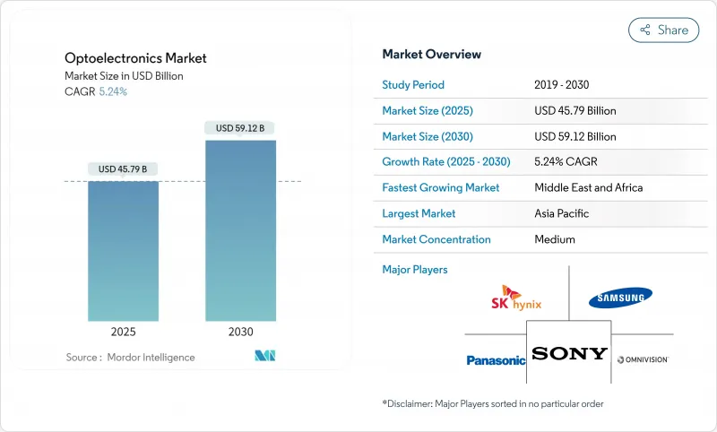
옵토일렉트로닉스 시장 규모는 2025년에 457억 9,000만 달러에 이르고, CAGR 5.24%를 나타내, 2030년에는 591억 2,000만 달러에 달할 것으로 예상됩니다.
수요는 폭넓게, 민생기기의 차세대 3D센싱, AI를 많이 사용하는 데이터센터의 고속광 링크, 전기차의 고도조명이나 화상시스템에 이릅니다. 기기의 기술 혁신은 고주파수와 온도에서 효율적으로 작동하는 광대역 갭 재료로부터 혜택을 받으며, 아시아와 북미의 정책 인센티브는 공급망의 탄력성을 강화하기 위해 지역 제조를 장려합니다. 메타서피스 옵틱스와 멀티 정션 VCSEL 아키텍처를 통합할 수 있는 기업은 특히 전력 효율과 컴팩트한 폼 팩터가 정수가 되는 경우 프리미엄 기회를 획득할 수 있는 입장에 있습니다. 모든 최종 용도에서 구매자는 중요한 입력의 추적 가능한 조달과 새로운 수출 관리 규칙을 준수하는 것을 증명할 수있는 능력으로 공급업체를 평가합니다.
세계의 옵토일렉트로닉스 시장 동향과 인사이트
아시아 스마트폰에서 VCSEL 기반 3D 감지 확산
안전한 얼굴 인증, 공간 비디오 캡처 및 실내 네비게이션에 대한 수요가 증가함에 따라 플래그십 터미널에서 수직 공진기면 발광 레이저의 역할이 강화되었습니다. 중국 벤더의 특허 출원은 VCSEL 스택을 완전히 국산화하고 수입 에피 웨이퍼에 대한 의존을 줄이려는 움직임을 보여줍니다. 높은 수율의 에피 성장과 고급 테스트 능력을 갖춘 부품 제조업체는 디스플레이 하에서 3D 센싱 전개에 앞서 다년간 공급 계약을 확보하고 있습니다. 광 AI 코프로세서의 성숙에 따라 옵토일렉트로닉스 시장에서는 VCSEL 대응의 제스처나 환경 매핑이 중위기종의 휴대전화에도 널리 채용될 것으로 예상되고 있습니다.
유럽에서 자동차 LED 조명의 엄격한 의무화
유럽 연합(EU)의 안전 기준은 눈부심을 최소화하고 야간 운전의 편안함을 향상시키는 적응형 LED 헤드라이트를 권장하며, 자동차 제조업체는 고급 라이트 도메인 컨트롤러의 채택을 추진하고 있습니다. Tier 1 공급업체는 역동적인 빔 성형, 브랜드 시그니처 애니메이션, 전기자동차의 항속 거리를 늘리는 에너지 절약을 가능하게 하는 RGB 매트릭스를 지원합니다. 설계 사이클에서는 냉각 질량을 늘리지 않고 루멘 출력과 규제 목표를 달성하기 위해 조명 팀과 열 팀의 긴밀한 협력이 점점 더 필요합니다. 모듈에 내장된 마이크로 옵틱스, 드라이버, 센서는 LED 다이 자체 이상의 가치를 추가하기 때문에 이 법은 간접적으로 옵토일렉트로닉스 시장을 뒷받침합니다. 유럽 모델을 호모로게이션하는 세계 자동차 제조업체들은 같은 첨단 조명 패키지를 다른 지역에도 보급하는 경향이 있어 유닛 수요를 확대하고 있습니다.
만성 GaN 기판 공급 제약
자립형 GaN 웨이퍼의 생산은 여전히 소수의 전문 시설에 집중되어 있으며 고출력 장치의 병목 현상이 되고 있습니다. 실리콘 상에 GaN을 성장시키는 현장적인 해결 방법은 비용 절감에 도움이 되지만 정격 전압을 제한하는 전위 밀도를 제공합니다. 정부는 현재 와이드 밴드갭 기판을 중요한 자산으로 취급하고 전략적 위험을 줄이기 위해 국내 결정 성장 공장에 세금 공제를 제공합니다. Qromis Substrate Technology와 같은 선구적인 접근법은 헤테로에피택셜 스택을 200mm 형식에 적응시켜 높은 처리량과 주류 팹과의 더 나은 호환성을 약속합니다. 이러한 조치는 중기적으로 생산 능력을 늘릴 것이지만 단기적인 생산 능력 부족은 계속 전기자동차 및 방어 프로그램에 우선적으로 할당하도록 촉구하고 있습니다.
부문 분석
LED는 원예용 조명, 자동차용 외장 모듈, 상업용 디스플레이가 회복되었기 때문에 2024년 옵토일렉트로닉스 시장에서 최대의 지위를 유지해 34%의 매출을 차지했습니다. 이 부문은 성숙한 생산 라인과 대규모 자본 강화 없이 와트당 루멘을 증가시키는 칩 수준의 개선으로 이익을 얻었습니다. 이와 병행하여, 레이저 다이오드, 특히 수직 공진기와 단면 발광 구조는 3D 센싱, 단거리 광 상호접속, 차재 LiDAR의 채용 확대에 의해 CAGR은 6.8%를 나타낼 전망입니다. 멀티 접합 아키텍처는 동일한 다이 면적에서 더 많은 광 파워를 끌어낼 수 있습니다. 휴대전화 제조업체가 턴키 이미터 패키지를 선호하기 때문에 웨이퍼 스케일 테스트와 통합 드라이버 IC를 결합한 공급업체는 여전히 설계 이점을 얻고 있습니다.
메타 서페이스 통합에 대한 관심 증가는 칩 표면에서 정확한 빔 성형의 가치를 증폭시켜 기기의 상대방 상표 제품 제조업체의 스위칭 비용을 증가시킵니다. 메타서피스 라이브러리가 성숙함에 따라 레이저 다이오드 설계자는 맞춤형 패터닝을 최종 에피택시 공정에 통합하여 기존 렌즈에서 달성할 수 없었던 패턴과 위상 제어를 실현합니다. 다이버전스 프로파일을 조정하는 능력은 AR 디스플레이 및 단초점 프로젝터에 대한 기업 수요를 개척하여 대응 가능한 옵토일렉트로닉스 시장의 총량을 확대합니다. LED는 여전히 대면적 조명에 필수적이지만, 레이저 다이오드는 코히런트 라이트와 타이트 빔 스티어링이 필수적인 프리미엄 틈새를 개척하고 있습니다.
질화갈륨은 뛰어난 전자 이동도와 열전도성으로 고속 스위칭에서 효율적인 동작이 가능해졌으며, 2024년 옵토일렉트로닉스 시장 점유율은 41%로 우위를 유지했습니다. 웨이퍼의 200mm로의 미세화는 비용 절감을 지원하고, 합금 엔지니어링은 센싱과 멸균을 위한 자외에서 가시광으로의 발광 조정을 실현합니다. 그러나 탄화규소는 CAGR 7.4%로 가장 빠른 성장 궤도를 나타내며, 그 3배 높은 열전도성은 급속 충전 전기자동차나 솔라 인버터용 파워 기기가 가능해지기 때문입니다. 미국과 유럽의 정부 지원에 의한 파일럿 라인에서는 현재 8인치 SiC 기판의 인정이 이루어지고 있어 양산을 위한 움직임이 활발해지고 있습니다.
인화 인듐은 직접 밴드 갭이 낮은 구동 전압에서 높은 변조 속도에 대응할 수 있기 때문에 400G를 넘는 데이터센터용 광학 부품으로서 다시 주목을 받고 있습니다. 갈륨 비소는 원격 조작 센서 및 비행 시간 센서의 적외선 이미 터의 주요 제품입니다. 한편, 실리콘 포토닉스는 CMOS 팹이나 하이브리드 레이저 어태치에 의해 III-V 웨이퍼 부족을 회피하고, 고밀도 트랜시버를 위한 비용 효율적인 솔루션으로 자리매김하고 있습니다. 이러한 추세를 종합하면 용도별 요구사항이 기판 선택을 결정하는 재료 다원주의가 부각되어 보다 광범위한 옵토일렉트로닉스 시장을 풍부하게 합니다.
지역 분석
아시아태평양은 옵토일렉트로닉스 시장의 52%를 차지하며 2024년 매출을 이끌었습니다. 이 리드는 깊은 공급망 통합, 경험이 풍부한 노동력, 오랜 정책 지원을 통해 구축되었습니다. 중국의 주조 능력은 지방 정부가 화합물 반도체에 특화된 200mm 및 300mm 팹에 보조금을 내는 것으로 성장을 계속하고 있습니다. 일본은 의료 영상 전문 지식을 활용하여 CMOS 센서 기반 진단 플랫폼을 개척하고 국내 수요를 높이는 한편, 서브 시스템을 유럽 및 북미에 수출하고 있습니다. 한국 디스플레이 벤더는 에피 결함 밀도를 줄이는 마이크로 LED 공정 노드를 추진하고 증강현실(AR)을 위한 새로운 고휘도 패널을 개발합니다. 대만은 지정 학적 위험에도 불구하고 첨단 패키징 스택에 필수적인 존재로 남아 있으며, 다국적 OEM에 동남아시아에서 두 번째 소스 조립의 다양화를 촉진하고 있습니다.
중동 및 아프리카은 2030년까지 연평균 복합 성장률(CAGR) 7.9%를 나타내, 국방 조달과 LED 조명, 파이버 백본, 보안 이미징을 통합한 스마트 시티의 거대 프로젝트가 그 원동력이 됩니다. 아랍에미리트(UAE)과 사우디아라비아는 석유 수출의 잉여를 주권 기술 클러스터로 향하게 하여 세계 옵토일렉트로닉스 기업에 지역 설계 센터의 설립을 호소하고 있습니다. 아프리카 해안 경제는 더 짧은 지상 링크를 지원하는 해저 섬유 육상국에 투자하여 패시브 옵틱스 수요와 하류 유지 보수 서비스를 자극합니다. 기본적인 수량은 아시아에 비해 겸손하지만, 높은 성장률에 의해 경계선 시스템용의 냉각식 중파 적외선 검출기 등, 틈새 기기의 채용이 가속하고 있습니다.
북미는 왕성한 벤처 자금, 강력한 대학 연구, 반도체 제조 및 연구 개발에 500억 달러를 충당하는 미국 CHIPS 장려금 덕분에 큰 옵토일렉트로닉스 시장의 영향력을 유지하고 있습니다. 국립 반도체 기술 센터는 포토닉스 신흥 기업의 진입 장벽을 낮추는 공유 프로토 타이핑 라인을 제공하고 수출 규제 업데이트는 듀얼 유스 IC 모니터링을 강화합니다. 캐나다는 얽힘 기반 통신을 탐구하는 양자 포토닉스 벤처를 육성하고 이 지역의 비즈니스 기회에 프론티어 분야를 추가하고 있습니다.
유럽은 반도체의 세계 점유율이 점차 저하되고 있는 것, 계측 광학, 차재 조명, 리소그래피 장치로 리더십을 유지하고 있습니다. 유럽 감사원은 추가 개입이 없으면 2030년 세계 점유율은 11.7%에 불과할 것으로 예측하고 있지만, Chips Act는 현지 생산 확대에 430억 유로를 할당하고 있습니다. 독일과 프랑스는 와이드 밴드갭 파워 기기의 파일럿 라인을 조정하고, 북유럽 국가들은 우주 및 방위 고객을 위한 화합물 반도체 에피택시를 확대하고 있습니다. 이 지역의 엄격한 환경 규제는 특히 빌딩 자동화에서 에너지 효율적인 옵토일렉트로닉스 부품 수요를 자극합니다.
남미는 광대역 확대, LED 가로등 프로그램, 브라질과 아르헨티나의 농업 이미징이 견인해, 규모는 작지만 옵토일렉트로닉스 시장에 있어서 성장 지역입니다. 국제 공급업체는 수입 관세를 피하고 현지 컨텐츠 요구 사항을 충족하기 위해 합작투자를 활용하여 향후 10년 동안 확장할 수 있는 생태계 능력을 육성하고 있습니다.
기타 혜택 :
- 엑셀 형식 시장 예측(ME) 시트
- 3개월간의 애널리스트 지원
목차
제1장 서론
- 조사 전제조건과 시장 정의
- 조사 범위
제2장 조사 방법
제3장 주요 요약
제4장 시장 상황
- 시장 개요
- 시장 성장 촉진요인
- 아시아 스마트폰에서 VCSEL 기반 3D 센싱의 보급
- 유럽에서 자동차용 LED 조명의 엄격한 규제
- 북미 데이터센터에서의 400G 파이버 모듈의 급속한 전개
- 동남아시아 스마트 시티 프로젝트에서 GaN LED에 대한 정부 인센티브
- 디지털 의료용 화상 기술의 붐이 일본의 CMOS 센서 시장을 견인
- 중동의 방위 근대화가 적외선 검출기 수요를 자극
- 시장 성장 억제요인
- 만성 GaN 기판 공급 제약
- 소비자용 VCSEL 어레이의 높은 열 관리 비용
- 첨단 이미지 센서 공급망의 수출 관리 장벽
- LED 가격 하락이 중국의 Tier 2 제조업체의 이익률을 압박
- 업계 생태계 분석
- 기술의 전망
- Porter's Five Forces 분석
- 공급기업의 협상력
- 구매자의 협상력
- 신규 참가업체의 위협
- 대체품의 위협
- 경쟁 기업 간 경쟁 관계
제5장 시장 규모와 성장 예측(금액관)
- 기기 유형별
- LED
- 레이저 다이오드
- 이미지 센서
- 옵토커플러
- 태양전지
- 기타
- 기기 소재별
- 질화 갈륨(GaN)
- 비소화 갈륨(GaAs)
- 실리콘 카바이드(SiC)
- 인듐 포스파이드(InP)
- 실리콘 및 기타
- 용도별
- 조명 및 디스플레이
- 광통신 및 Li-Fi
- 센싱 및 이미징
- 전력 변환 및 태양광 발전
- 국방 및 보안
- 최종 사용자 업계별
- 가전
- 자동차
- 정보기술 및 통신
- 헬스케어 및 생명과학
- 항공우주 및 방위
- 산업 자동화
- 주택 및 상업시설
- 지역별
- 북미
- 미국
- 캐나다
- 멕시코
- 유럽
- 독일
- 영국
- 프랑스
- 이탈리아
- 스페인
- 기타 유럽
- 아시아태평양
- 중국
- 일본
- 한국
- 인도
- 동남아시아
- 호주
- 기타 아시아태평양
- 남미
- 브라질
- 기타 남미
- 중동 및 아프리카
- 중동
- 아랍에미리트(UAE)
- 사우디아라비아
- 기타 중동
- 아프리카
- 남아프리카
- 기타 아프리카
- 북미
제6장 경쟁 구도
- 시장 집중도
- 전략적 동향
- 시장 점유율 분석
- 기업 프로파일
- Sony Corporation
- Samsung Electronics Co., Ltd.
- ams-OSRAM AG
- SK Hynix Inc.
- Broadcom Inc.
- Panasonic Holdings Corp.
- Signify NV
- Nichia Corporation
- Texas Instruments Inc.
- STMicroelectronics NV
- Infineon Technologies AG
- ON Semiconductor Corp.
- Vishay Intertechnology Inc.
- Renesas Electronics Corp.
- Rohm Co., Ltd.
- Omnivision Technologies Inc.
- Cree LED(Wolfspeed, Inc.)
- LITE-ON Technology Corp.
- Sharp Corporation
- Mitsubishi Electric Corp.
제7장 시장 기회와 향후 전망
KTH 25.11.04The optoelectronics market size reached USD 45.79 billion in 2025 and is forecast to climb to USD 59.12 billion by 2030 as it advances at a 5.24% CAGR.

Demand is broad-based, spanning next-generation 3D sensing in consumer devices, higher-speed optical links for AI-heavy data centers, and advanced lighting and imaging systems in electric vehicles. Device innovation benefits from wide-bandgap materials that operate efficiently at elevated frequencies and temperatures, while policy incentives in Asia and North America encourage regional fabrication to bolster supply-chain resilience. Companies able to integrate metasurface optics or multi-junction VCSEL architectures are positioned to capture premium opportunities, especially where power efficiency and compact form factors are decisive. Across all end uses, buyers increasingly evaluate suppliers on the ability to certify both traceable sourcing of critical inputs and compliance with emerging export-control rules, factors that now influence design-win decisions as much as raw performance.
Global Optoelectronics Market Trends and Insights
Proliferation of VCSEL-based 3D sensing in Asian smartphones
Rising demand for secure facial authentication, spatial video capture, and indoor navigation is reinforcing the role of vertical-cavity surface-emitting lasers in flagship handsets. Major brands integrate multi-junction VCSEL arrays that raise optical power while cutting battery drain, ultimately improving user experience.Patent filings by Chinese vendors illustrate a push to localize the full VCSEL stack and reduce dependence on imported epi-wafers, a move aligned with broader semiconductor self-reliance goals. Component suppliers positioned with high-yield epi-growth and advanced testing capacity are securing multi-year supply agreements ahead of under-display 3D sensing roll-outs. As optical-AI co-processors mature, the optoelectronics market anticipates wider adoption of VCSEL-enabled gesture and environment mapping across mid-tier phones as well.
Stringent automotive LED-lighting mandates in Europe
European Union safety standards now favor adaptive LED headlights that minimize glare and improve night driving comfort, pushing carmakers to adopt sophisticated light-domain controllers.Tier-1 suppliers respond with RGB matrices that enable dynamic beam shaping, brand-signature animations, and energy savings that extend electric-vehicle range. Design cycles increasingly require close collaboration between lighting and thermal teams to meet lumen output and regulation targets without adding cooling mass. The legislation indirectly boosts the optoelectronics market because micro-optics, drivers, and sensors embedded in the modules add value beyond the LED die itself. Global automakers homologating models for Europe tend to propagate the same advanced lighting packages into other regions, broadening unit demand.
Chronic GaN-substrate supply constraints
Production of free-standing GaN wafers remains concentrated in a handful of specialized facilities, creating bottlenecks for high-power devices. Makeshift workarounds such as growing GaN on silicon help lower costs but introduce dislocation densities that limit voltage ratings. Governments now treat wide-bandgap substrates as critical assets, offering tax credits for domestic crystal-growth plants to ease strategic risk. Pioneering approaches like Qromis Substrate Technology adapt hetero-epitaxial stacks to 200 mm formats, promising higher throughput and better compatibility with mainstream fabs. While these measures will add capacity over the medium term, short-term shortages continue to prompt allocation prioritization in favor of electric-vehicle and defense programs.
Other drivers and restraints analyzed in the detailed report include:
- Rapid roll-out of 400 G fiber modules in North-American data centers
- Government incentives for GaN LEDs in Southeast-Asian smart-city projects
- High thermal-management cost of consumer VCSEL arrays
For complete list of drivers and restraints, kindly check the Table Of Contents.
Segment Analysis
LEDs retained the largest position in the 2024 optoelectronics market, accounting for 34% revenue as horticulture lighting, automotive exterior modules, and commercial displays rebounded. The segment benefited from mature manufacturing lines and incremental chip-level improvements that squeezed more lumens per watt without major capital upgrades. In parallel, laser diodes-especially vertical-cavity and edge-emitting structures-advanced at a 6.8% CAGR outlook due to expanding 3D sensing, short-reach optical interconnect, and automotive LiDAR adoption. Multi-junction architectures now squeeze additional optical power from the same die area, a feature critical for under-display projectors where footprint is limited. Suppliers that combine wafer-scale testing with integrated driver ICs continue to gain design wins as handset makers favor turnkey emitter packages.
Rising interest in metasurface integration amplifies the value of precise beam shaping at the chip face, which in turn raises switching costs for device original equipment manufacturers. As metasurface libraries mature, laser-diode designers embed custom patterning in the final epitaxy step, delivering pattern and phase control unattainable with conventional lenses. The ability to tailor divergence profiles opens enterprise demand for AR displays and short-throw projectors, widening the total addressable optoelectronics market. LEDs will remain indispensable for large-area illumination, yet laser diodes are carving out premium niches where coherent light or tight beam steering is essential.
Gallium nitride maintained dominance in 2024 with a 41% optoelectronics market share, sustained by its superior electron mobility and thermal conductivity that allow efficient operation at high switching speeds. Wafer scaling to 200 mm supports cost reductions, while alloy engineering delivers ultraviolet-to-visible emission tuning for sensing and sterilization. However, silicon carbide exhibits the fastest growth trajectory at a 7.4% CAGR as its threefold higher thermal conductivity enables power devices for fast-charging electric vehicles and solar inverters. Government-backed pilot lines in the United States and Europe now qualify 8-inch SiC substrates, signaling a ramp toward mass production.
Indium phosphide garners renewed attention for data-center optics beyond 400 G because its direct bandgap accommodates high-modulation speeds with low drive voltage. Gallium arsenide remains the workhorse for infrared emitters in remote-control and time-of-flight sensors. Meanwhile, silicon photonics positions itself as a cost-effective solution for dense transceivers, leveraging CMOS fabs and hybrid laser attach to sidestep III-V wafer shortages. Collectively, these trends underscore material pluralism wherein application-specific requirements dictate substrate selection, enriching the broader optoelectronics market.
The Optoelectronics Market Report is Segmented by Device Type (LED, Laser Diode, Image Sensors, and More), Device Material (Gallium Nitride (GaN), Gallium Arsenide (GaAs), Silicon Carbide (SiC), and More), Application (Lighting and Display, Sensing and Imaging, and More), End-User Industry (Automotive, Aerospace and Defense, Consumer Electronics, and More), and Geography. The Market Forecasts are Provided in Terms of Value (USD).
Geography Analysis
Asia Pacific dominates the optoelectronics market with 52% of 2024 revenue, a lead built on deep supply-chain integration, experienced labor, and long-standing policy support. China's foundry capacity continues to grow as provincial governments subsidize 200 mm and 300 mm fabs that focus on compound semiconductors, an expansion that mitigates some substrate shortages yet also raises concerns about overcapacity. Japan leverages its medical-imaging expertise to pioneer CMOS-sensor-based diagnostic platforms, boosting domestic demand while exporting subsystems to Europe and North America. South Korea's display vendors push micro-LED process nodes that shrink epi-defect density, creating new high-brightness panels for augmented reality. Taiwan remains indispensable in the advanced-packaging stack despite geopolitical risk, prompting multinational OEMs to diversify second-source assembly in Southeast Asia.
The Middle East and Africa region posts a 7.9% CAGR outlook through 2030, fueled by national defense procurements and smart-city megaprojects that integrate LED lighting, fiber backbones, and security imaging. United Arab Emirates and Saudi Arabia channel oil-export surpluses into sovereign technology clusters, inviting global optoelectronic players to establish regional design centers. African coastal economies invest in submarine fiber landing stations that anchor shorter terrestrial links, stimulating passive-optics demand and downstream maintenance services. Although base volumes remain modest compared with Asia, high growth accelerates adoption of niche devices such as cooled mid-wave IR detectors for perimeter systems.
North America sustains substantial optoelectronics market influence thanks to robust venture funding, strong university research, and the U.S. CHIPS incentive that earmarks USD 50 billion for semiconductor manufacturing and R&D. The National Semiconductor Technology Center provides shared prototyping lines that lower barrier-to-entry for photonics start-ups, while export-control updates tighten oversight of dual-use ICs. Canada nurtures quantum-photonics ventures that explore entanglement-based communication, adding a frontier segment to the regional opportunity set.
Europe contends with a gradual erosion of global semiconductor share yet retains leadership in metrology optics, automotive lighting, and lithography equipment. The Chips Act allocates EUR 43 billion to amplify local production, though the European Court of Auditors projects only 11.7% global share by 2030 absent further interventions. Germany and France coordinate pilot lines for wide-bandgap power devices, while Nordic nations expand compound-semiconductor epitaxy dedicated to space and defense customers. The region's stringent environmental rules stimulate demand for energy-efficient optoelectronic components, particularly in building automation.
South America remains a smaller but rising geography for the optoelectronics market, driven by broadband expansion, LED street-lighting programs, and agricultural imaging in Brazil and Argentina. International suppliers use joint-ventures to sidestep import duties and meet local-content requirements, seeding ecosystem capability that could scale in the next decade.
- Sony Corporation
- Samsung Electronics Co., Ltd.
- ams-OSRAM AG
- SK Hynix Inc.
- Broadcom Inc.
- Panasonic Holdings Corp.
- Signify N.V.
- Nichia Corporation
- Texas Instruments Inc.
- STMicroelectronics N.V.
- Infineon Technologies AG
- ON Semiconductor Corp.
- Vishay Intertechnology Inc.
- Renesas Electronics Corp.
- Rohm Co., Ltd.
- Omnivision Technologies Inc.
- Cree LED (Wolfspeed, Inc.)
- LITE-ON Technology Corp.
- Sharp Corporation
- Mitsubishi Electric Corp.
Additional Benefits:
- The market estimate (ME) sheet in Excel format
- 3 months of analyst support
TABLE OF CONTENTS
1 INTRODUCTION
- 1.1 Study Assumptions and Market Definition
- 1.2 Scope of the Study
2 RESEARCH METHODOLOGY
3 EXECUTIVE SUMMARY
4 MARKET LANDSCAPE
- 4.1 Market Overview
- 4.2 Market Drivers
- 4.2.1 Proliferation of VCSEL-based 3-D Sensing in Asian Smartphones
- 4.2.2 Stringent Automotive LED-Lighting Mandates in Europe
- 4.2.3 Rapid Roll-out of 400 G Fiber Modules in North-American Data Centers
- 4.2.4 Government Incentives for GaN LEDs in SE-Asian Smart-City Projects
- 4.2.5 Digital Medical Imaging Boom Driving CMOS Sensors in Japan
- 4.2.6 Middle-East Defense Modernization Fueling Infra-red Detector Demand
- 4.3 Market Restraints
- 4.3.1 Chronic GaN-substrate Supply Constraints
- 4.3.2 High Thermal-management Cost of Consumer VCSEL Arrays
- 4.3.3 Export-control Barriers on Advanced Image-Sensor Supply Chains
- 4.3.4 LED Price-Erosion Compressing Tier-2 Chinese Margins
- 4.4 Industry Ecosystem Analysis
- 4.5 Technological Outlook
- 4.6 Porter's Five Forces Analysis
- 4.6.1 Bargaining Power of Suppliers
- 4.6.2 Bargaining Power of Buyers
- 4.6.3 Threat of New Entrants
- 4.6.4 Threat of Substitutes
- 4.6.5 Intensity of Competitive Rivalry
5 MARKET SIZE AND GROWTH FORECASTS (VALUES)
- 5.1 By Device Type
- 5.1.1 LED
- 5.1.2 Laser Diode
- 5.1.3 Image Sensors
- 5.1.4 Optocouplers
- 5.1.5 Photovoltaic Cells
- 5.1.6 Others
- 5.2 By Device Material
- 5.2.1 Gallium Nitride (GaN)
- 5.2.2 Gallium Arsenide (GaAs)
- 5.2.3 Silicon Carbide (SiC)
- 5.2.4 Indium Phosphide (InP)
- 5.2.5 Silicon and Others
- 5.3 By Application
- 5.3.1 Lighting and Display
- 5.3.2 Optical Communication and Li-Fi
- 5.3.3 Sensing and Imaging
- 5.3.4 Power Conversion and Photovoltaics
- 5.3.5 Defense and Security
- 5.4 By End-user Industry
- 5.4.1 Consumer Electronics
- 5.4.2 Automotive
- 5.4.3 Information Technology and Telecom
- 5.4.4 Healthcare and Life-Sciences
- 5.4.5 Aerospace and Defense
- 5.4.6 Industrial Automation
- 5.4.7 Residential and Commercial
- 5.5 By Geography
- 5.5.1 North America
- 5.5.1.1 United States
- 5.5.1.2 Canada
- 5.5.1.3 Mexico
- 5.5.2 Europe
- 5.5.2.1 Germany
- 5.5.2.2 United Kingdom
- 5.5.2.3 France
- 5.5.2.4 Italy
- 5.5.2.5 Spain
- 5.5.2.6 Rest of Europe
- 5.5.3 Asia-Pacific
- 5.5.3.1 China
- 5.5.3.2 Japan
- 5.5.3.3 South Korea
- 5.5.3.4 India
- 5.5.3.5 South East Asia
- 5.5.3.6 Australia
- 5.5.3.7 Rest of Asia-Pacific
- 5.5.4 South America
- 5.5.4.1 Brazil
- 5.5.4.2 Rest of South America
- 5.5.5 Middle East and Africa
- 5.5.5.1 Middle East
- 5.5.5.1.1 United Arab Emirates
- 5.5.5.1.2 Saudi Arabia
- 5.5.5.1.3 Rest of Middle East
- 5.5.5.2 Africa
- 5.5.5.2.1 South Africa
- 5.5.5.2.2 Rest of Africa
- 5.5.1 North America
6 COMPETITIVE LANDSCAPE
- 6.1 Market Concentration
- 6.2 Strategic Moves
- 6.3 Market Share Analysis
- 6.4 Company Profiles {(includes Global level Overview, Market level overview, Core Segments, Financials as available, Strategic Information, Market Rank/Share for key companies, Products and Services, and Recent Developments)}
- 6.4.1 Sony Corporation
- 6.4.2 Samsung Electronics Co., Ltd.
- 6.4.3 ams-OSRAM AG
- 6.4.4 SK Hynix Inc.
- 6.4.5 Broadcom Inc.
- 6.4.6 Panasonic Holdings Corp.
- 6.4.7 Signify N.V.
- 6.4.8 Nichia Corporation
- 6.4.9 Texas Instruments Inc.
- 6.4.10 STMicroelectronics N.V.
- 6.4.11 Infineon Technologies AG
- 6.4.12 ON Semiconductor Corp.
- 6.4.13 Vishay Intertechnology Inc.
- 6.4.14 Renesas Electronics Corp.
- 6.4.15 Rohm Co., Ltd.
- 6.4.16 Omnivision Technologies Inc.
- 6.4.17 Cree LED (Wolfspeed, Inc.)
- 6.4.18 LITE-ON Technology Corp.
- 6.4.19 Sharp Corporation
- 6.4.20 Mitsubishi Electric Corp.
7 MARKET OPPORTUNITIES AND FUTURE OUTLOOK
- 7.1 White-space and Unmet-Need Assessment
