


|
시장보고서
상품코드
1851086
SLP(Substrate Like PCB) 시장 : 시장 점유율 분석, 산업 동향, 통계, 성장 예측(2025-2030년)Substrate-Like-PCB - Market Share Analysis, Industry Trends & Statistics, Growth Forecasts (2025 - 2030) |
||||||
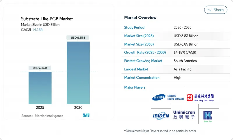
SLP(Substrate Like PCB) 시장 규모는 2025년에 35억 3,000만 달러로 추정되고, 2030년에는 68억 5,000만 달러로 확대될 것으로 예측되며, CAGR 14.18%로 성장할 전망입니다.
OEM이 기존의 고밀도 인터커넥트 보드에서 반도체 패키징으로 완전히 전환하지 않고 IC 보드 레벨 배선 밀도를 실현하는 솔루션으로 전환함에 따라 수요가 가속화됩니다. 수량 성장은 신호 무결성을 위해 25마이크로미터 이하 라인/스페이스 지오메트리를 필요로 하는 5G 라디오, 인공지능 프로세서 및 차량 탑재 ADAS 컨트롤러에 집중되어 있습니다. 아시아태평양은 반도체 파운드리 및 PCB 패브리케이터 간의 긴밀한 협력과 개선된 세미 애디티브 프로세싱 라인에 대한 지속적인 투자로 2024년 매출의 69%를 차지했습니다. ABF 빌드업 필름은 저손실 유전 특성을 강력하게 재료 선택을 지배하고 있지만, 공급 기반이 집중되어 있기 때문에 티아완 패브리케이터에 의한 수직 통합의 움직임이 활발해지고 있습니다. 25마이크로미터 이하의 수율 최적화는 AI를 활용한 검사에 의존하는 경향이 강해지고 있으며, 프로세스 제어의 리더는 구조적인 비용 우위를 획득하고 있습니다. 미국 국방부의 3,000만 달러의 보조금 등 지정학적 리쇼어링의 인센티브는 신규 진출기업의 자격 요건을 엄격하게 하는 한편, 지역의 다양화를 가져옵니다.
세계의 SLP(Substrate Like PCB) 시장 동향 및 인사이트
스마트폰 OEM에 의한 고밀도 상호접속 채용 급증
벤더는 SLP(Substrate Like PCB) 시장 기술을 이용해 회로 밀도를 약 30% 향상시켜 디바이스 두께를 평평하게 유지하면서 5G 모뎀, AI 코프로세서, 멀티렌즈 카메라 제어를 위한 공간을 확대했습니다. 플래그십 모델의 스케일 메리트는 중위기종의 휴대전화에도 흘러들어 보다 폭넓은 포트폴리오에서 자본 비용을 상각하는 대량 생산을 유지합니다.
5G 통신 모듈 수요 증가
mm파 베이스 스테이션 보드 및 소비자용 5G 무선 카드는 삽입 손실과 크로스토크를 억제하기 위해 25마이크로미터 이하 배선이 필요합니다. 네트워크 OEM은 매시브 MIMO 어레이 및 빔포밍 프론트엔드용 SLP(Substrate Like PCB) 시장 설계를 지정하여 기판 밀도와 스펙트럼 효율 목표를 연결합니다. 동일한 설계 규칙은 예상되는 데이터 속도가 증가함에 따라 스마트폰 및 태블릿으로 이동합니다.
SLP 생산 라인의 높은 CAPEX
그린필드 SLP(Substrate Like PCB) 시장 라인은 정밀 레이저 드릴, 직접 이미지 포토리소그래피, 클래스 1000의 클린룸 공간이 필요합니다. 1억 달러의 지출은 소규모 패브리케이터에게 합작투자의 설립 및 철수를 강요해 밸런스 시트의 두께를 자랑하는 기존 기업에 생산 능력을 집약시킵니다.
부문 분석
스마트폰은 2024년 SLP(Substrate Like PCB) 시장 수익의 47%를 차지했으며, 2025년에도 계속해서 주요 고객입니다. 이 부문은 세계 휴대전화 출하에 내재하는 SLP(Substrate Like PCB) 시장 규모의 우위성을 활용하여 급속한 생산능력 증강을 담당합니다. AI 엔진과 5안테나 5G 라디오를 결합한 프리미엄 디바이스는 25마이크로미터 이하 배선이 필요하며 최첨단 수요를 강화합니다. 그 후, 비용 곡선이 연쇄적으로 변화함으로써, 플래그쉽의 리프레시를 넘은 볼륨 가시성이 확대되어, 중위층의 채용이 가능하게 됩니다.
웨어러블은 CAGR 15.4%에서 가장 급성장하는 틈새 분야이며, 건강 모니터링의 의무화 및 증강현실 헤드셋에 의해 촉진됩니다. 공급업체는 고효율 전원 관리 IC를 기판에 직접 통합하여 에너지 밀도를 최적화하고 SLP의 0.5mm 이하 비아 피치의 가치를 입증합니다. Automotive Electronics는 OEM이 중복 센서 융합 보드를 지정하여 수익원을 다양화합니다. 네트워킹 인프라와 엣지 컴퓨팅 게이트웨이는 열 및 대기 시간 목표를 달성하기 위해 SLP를 채택하고 산업 및 의료 시스템은 엄격한 신뢰성으로 프리미엄 ASP를 획득했습니다.
10-12층은 2024년 생산량의 37%를 차지했으며, 배선 헤드룸과 관리 가능한 수율 리스크의 균형을 맞추고 있습니다. 이 계층은 스마트폰 기판과 관련된 SLP(Substrate Like PCB) 시장 규모의 주력입니다. 12층이 넘는 디자인은 칩렛 기반의 AI 가속기와 자동차 도메인 컨트롤러를 배경으로 CAGR 13%로 확대되고 있습니다. 여기서 'SLP(Substrate Like PCB) 시장 점유율'은 연속적인 라미네이션 사이클에서 누적 워프 제어를 마스터하는 패브리케이터에 가져옵니다. 레이어 수는 8-10으로, 비용에 중점을 둔 소비자용 IoT 제품에 대응하고 SLP를 향해 기술할 수 있는 HDI 벤더에게 엔트리 경로를 제공합니다.
SLP(Substrate Like PCB) 시장은 용도별(스마트폰, 태블릿, 웨어러블, 카 일렉트로닉스, 기타), 적층수별(8-10층, 10-12층, 기타), 기재별(ABF, 변성 에폭시/FR-4, 기타), 라인 및 스페이스 해상도별(30/30mm, 25/25mm, 20/20mm 이하), 지역별로 분류되어 있습니다. 시장 예측은 금액(달러)으로 제공됩니다.
지역별 분석
아시아태평양은 대만, 한국, 일본을 중심으로 2024년 매출 점유율 69%를 유지했습니다. 주조에 인접한 에코시스템은 PCB 벤더가 반도체 고객으로부터 연구개발을 공동 이용함으로써 제조를 위한 설계 사이클을 가속시킵니다. 중국의 패브리케이터는 생산 능력을 적극적으로 확대하고 있습니다. Zhen Ding은 2024년에 23%의 톱라인 성장을 기록했으며, 2027년까지 IC기판 수익의 CAGR 50%를 향해 방향타를 끊고 있습니다. 일본의 재료 메이저는 ABF 필름을 이 지역에 공급하여 지역 공급망 밀도를 강화하고 있습니다.
북미의 2024년 기여율은 18%였지만, 3,000만 달러의 국방자금과 CHIPS법의 우대조치의 혜택을 받고 있으며, 선진적인 투어링 비용을 부담하고 있습니다. TTM Technologies의 시러큐스 시설은 1억 3,000만 달러로 북미 대륙에서 가장 큰 초HDI 투자이며 보안 공급 방어 워크로드를 대상으로 합니다. 자동차의 전기화 및 사설망 5G의 전개는 이 지역 수요에 구조적인 발판을 줍니다.
유럽의 소규모이면서도 전략적인 실적는 AT&S가 주도하고 있어, ADAS 보드를 필요로 하는 독일의 OEM에 서비스를 제공하기 위해 말레이시아에서의 생산을 확대했습니다. 기술 주권을 목표로 하는 EU 보조금은 특히 자동차 및 의료 분야를 위한 SLP 라인의 증설을 지원합니다.
남미는 저수준에서 시작되었지만, 니어 쇼어링에 의해 경조립이 도미니카 공화국과 멕시코로 이동하여 CAGR 12.2%를 기록했습니다. 정부는 고용 창출을 위해 전자 클러스터를 추진하고 자유 무역 협정에 따른 파일럿 SLP 투자를 유치하고 있습니다.
중동 및 아프리카는 아직 발전도상이지만 정부계 다양화 펀드가 반도체 백엔드 에코시스템에 자본을 투입함으로써 업사이드를 유지하고, 지역의 디자인하우스가 성숙하면 미래의 SLP(Substrate Like PCB) 시장에 침투할 수 있게 됩니다.
기타 혜택 :
- 엑셀 형식 시장 예측(ME) 시트
- 3개월의 애널리스트 서포트
목차
제1장 서론
- 조사의 전제조건 및 시장 정의
- 조사 범위
제2장 조사 방법
제3장 주요 요약
제4장 시장 상황
- 시장 개요
- 시장 성장 촉진요인
- 고밀도 상호 접속에 대한 스마트폰 OEM 채용 급증
- 5G 통신 모듈 수요 증가
- 웨어러블 및 IoT 디바이스의 소형화 동향
- 프린트 기판의 복잡화가 진행되는 차재 ADAS 및 EV 일렉트로닉스
- 이종 집적을 가능하게 하는 SLP상의 플립칩
- 온쇼어 첨단 PCB 팹에 대한 정부 보조금
- 시장 성장 억제요인
- SLP 제조 라인의 CAPEX가 상승
- 25mL/S 미만에 있어서 공정 수율의 과제
- 특수 빌드업 화학물질에 관한 환경규제
- 벤더가 제한됨에 의한 ABF 수지 공급 위험
- 밸류체인 및 공급망 분석
- 규제 상황
- 기술의 전망
- Porter's Five Forces
- 공급기업의 협상력
- 구매자의 협상력
- 신규 참가업체의 위협
- 대체품의 위협
- 경쟁의 격렬함
- 업계 밸류체인 분석
제5장 시장 규모 및 성장 예측
- 용도별
- 스마트폰
- 태블릿
- 웨어러블
- 자동차 일렉트로닉스
- 네트워크 및 통신 인프라
- IoT 및 엣지 디바이스
- 산업용 및 의료용 일렉트로닉스
- 빌드업 층수별
- 8-10층
- 10-12층
- 12층 이상
- 기재별
- ABF(아지노모토 빌드업 필름)
- 변성 에폭시/FR-4
- 기타(PTFE, BT레진)
- 라인 및 스페이스 해상도별
- 30/30마이크로미터
- 25/25마이크로미터
- 20/20마이크로미터
- 지역별
- 북미
- 미국
- 캐나다
- 멕시코
- 남미
- 브라질
- 아르헨티나
- 기타 남미
- 유럽
- 영국
- 독일
- 프랑스
- 이탈리아
- 스페인
- 러시아
- 기타 유럽
- 아시아태평양
- 중국
- 일본
- 한국
- 인도
- 호주
- 기타 아시아태평양
- 중동 및 아프리카
- GCC
- 남아프리카
- 기타 중동 및 아프리카
- 북미
제6장 경쟁 구도
- 시장 집중도
- 전략적 동향
- 시장 점유율 분석
- 기업 프로파일
- Kinsus Interconnect Technology Corp.
- Ibiden Co., Ltd.
- Compeq Manufacturing Co., Ltd.
- Daeduck Electronics Co., Ltd.
- Unimicron Technology Corp.
- Zhen Ding Technology Holding
- TTM Technologies
- Meiko Electronics Co., Ltd.
- ATandS AG
- Korea Circuit Co., Ltd.
- LG Innotek Co., Ltd.
- Samsung Electro-Mechanics
- Shennan Circuits Co., Ltd.
- Tripod Technology
- Fujitsu Interconnect
- Wus Printed Circuit
- HannStar Board Corp.
- Nippon Mektron Ltd.
- NCAB Group AB
- Multek Ltd.
제7장 시장 기회 및 향후 전망
AJY 25.11.12The Substrate-Like PCB market size reached USD 3.53 billion in 2025 and is forecast to advance to USD 6.85 billion by 2030, reflecting a 14.18% CAGR.

Demand accelerates as OEMs migrate from conventional high-density interconnect boards to solutions that deliver IC-substrate-level wiring density without fully moving into semiconductor packaging. Volume growth is anchored in 5G radio, artificial-intelligence processors, and automotive ADAS controllers that require <=25 µm line/space geometries for signal integrity. Asia-Pacific captured 69% of revenue in 2024, benefiting from tight linkages between semiconductor foundries and PCB fabricators plus sustained investment in modified semi-additive processing lines . ABF build-up films dominate material selection on the strength of low-loss dielectric properties, though their concentrated supply base prompts vertical-integration moves by tier-one fabricators. Yield optimization below 25 µm increasingly hinges on AI-enabled inspection, giving process-control leaders a structural cost advantage. Geopolitical reshoring incentives-such as the USD 30 million U.S. Department of Defense grant-add regional diversification while tightening qualification hurdles for new entrants.
Global Substrate-Like-PCB Market Trends and Insights
Surging smartphone OEM adoption for high-density interconnects
Premium handset vendors used Substrate-Like PCB market technology to raise circuit density by roughly 30%, unlocking more space for 5G modems, AI coprocessors, and multi-lens camera control while holding device thickness flat. Scale benefits from flagship models flow into mid-tier phones, sustaining high production runs that amortize capital costs across broader portfolios.
Rising demand for 5G communication modules
Millimeter-wave base-station boards and consumer 5G radio cards require <=25 µm routing to curb insertion loss and crosstalk. Network OEMs specify Substrate-Like PCB market designs for massive-MIMO arrays and beam-forming front ends, linking board density with spectral-efficiency targets. The same design rules migrate into smartphones and tablets as data-rate expectations climb.
High CAPEX for SLP production lines
A greenfield Substrate-Like PCB market line requires precision laser drills, direct-imaging photolithography, and Class 1000 cleanroom space. The USD 100 million outlay pressures smaller fabricators to form joint ventures or exit, consolidating capacity with incumbents that boast balance-sheet depth.
Other drivers and restraints analyzed in the detailed report include:
- Miniaturization trends in wearables & IoT devices
- Automotive ADAS & EV electronics escalating PCB complexity
- Process-yield challenges at <25 µm L/S
For complete list of drivers and restraints, kindly check the Table Of Contents.
Segment Analysis
Smartphones accounted for 47% of Substrate-Like PCB market revenue in 2024 and remain the anchor customer set entering 2025. The segment leverages the Substrate-Like PCB market size advantage inherent in global handset shipments to underwrite rapid capacity ramps. Premium devices that pair AI engines with 5-antenna 5G radios require <=25 µm wiring, reinforcing demand at the leading edge. A cascading cost curve then enables mid-tier adoption, extending volume visibility beyond flagship refreshes.
Wearables are the fastest-growing niche at a 15.4% CAGR, catalyzed by health monitoring mandates and augmented-reality headsets. Suppliers optimize energy density by embedding high-efficiency power-management ICs directly onto the board, proving the value of SLP's sub-0.5 mm via pitch. Automotive electronics add diversified revenue streams as OEMs specify redundant sensor-fusion boards. Networking infrastructure and edge-computing gateways adopt SLP to meet thermal and latency targets, while industrial and medical systems command premium ASPs due to stringent reliability.
The 10-12-layer cohort controlled 37% of 2024 output, balancing routing headroom with manageable yield risk. This stratum remains the workhorse for the Substrate-Like PCB market size tied to smartphone boards. Designs exceeding 12 layers are scaling at 13% CAGR on the back of chiplet-based AI accelerators and automotive domain controllers. Here, "Substrate-Like PCB market share" accrues to fabricators that master cumulative-warp control across sequential lamination cycles. Layer counts of 8-10 serve cost-sensitive consumer IoT products, offering an entry path for HDI vendors up-skilling toward SLP.
Substrate-Like-PCB Market is Segmented by Application (Smartphones, Tablets, Wearables, Automotive Electronics, and More), by Build-Up Layer Count (8 - 10 Layers, 10 - 12 Layers, and More), by Base Material (ABF, Modified Epoxy / FR-4, and More), by Line/Space Resolution (30/30 Mm, 25/25 Mm, and <= 20/20 Mm) and by Geography. The Market Forecasts are Provided in Terms of Value (USD).
Geography Analysis
Asia-Pacific retained a 69% revenue share in 2024, anchored by Taiwan, South Korea, and Japan. Foundry-adjacent ecosystems accelerate design-for-manufacture cycles, letting PCB vendors co-opt R&D from semiconductor customers. Chinese fabricators expand capacity aggressively; Zhen Ding booked 23% top-line growth in 2024 and is steering toward 50% CAGR in IC-substrate revenue through 2027. Material majors in Japan supply ABF films to the region, reinforcing local supply-chain density.
North America contributed 18% in 2024 but benefits from USD 30 million defense funding plus CHIPS Act incentives that defray advanced tooling. TTM Technologies' USD 130 million Syracuse facility constitutes the largest ultra-HDI investment on the continent, targeting secure-supply defense workloads. Automotive electrification and private-network 5G rollouts give regional demand a structural leg.
Europe's smaller yet strategic footprint is led by AT&S, which extended Malaysian production to serve German OEMs needing ADAS boards. EU grants targeting technology sovereignty support incremental SLP lines, especially for automotive and medical verticals.
South America, though starting from a low base, records a 12.2% CAGR as near-shoring shifts light assembly to the Dominican Republic and Mexico. Governments promote electronics clusters for job creation, drawing pilot SLP investment to align with free-trade agreements.
The Middle East and Africa remain nascent but preserve upside through sovereign diversification funds channeling capital into semiconductor back-end ecosystems, enabling future Substrate-Like PCB market penetration once regional design houses mature.
- Kinsus Interconnect Technology Corp.
- Ibiden Co., Ltd.
- Compeq Manufacturing Co., Ltd.
- Daeduck Electronics Co., Ltd.
- Unimicron Technology Corp.
- Zhen Ding Technology Holding
- TTM Technologies
- Meiko Electronics Co., Ltd.
- ATandS AG
- Korea Circuit Co., Ltd.
- LG Innotek Co., Ltd.
- Samsung Electro-Mechanics
- Shennan Circuits Co., Ltd.
- Tripod Technology
- Fujitsu Interconnect
- Wus Printed Circuit
- HannStar Board Corp.
- Nippon Mektron Ltd.
- NCAB Group AB
- Multek Ltd.
Additional Benefits:
- The market estimate (ME) sheet in Excel format
- 3 months of analyst support
TABLE OF CONTENTS
1 INTRODUCTION
- 1.1 Study Assumptions and Market Definition
- 1.2 Scope of the Study
2 RESEARCH METHODOLOGY
3 EXECUTIVE SUMMARY
4 MARKET LANDSCAPE
- 4.1 Market Overview
- 4.2 Market Drivers
- 4.2.1 Surging smartphone OEM adoption for high-density interconnects
- 4.2.2 Rising demand for 5G communication modules
- 4.2.3 Miniaturization trends in wearables and IoT devices
- 4.2.4 Automotive ADAS and EV electronics escalating PCB complexity
- 4.2.5 Flip-chip on SLP enabling heterogeneous integration
- 4.2.6 Government subsidies for on-shore advanced PCB fabs
- 4.3 Market Restraints
- 4.3.1 High CAPEX for SLP production lines
- 4.3.2 Process-yield challenges at <25 m L/S
- 4.3.3 Environmental rules on specialty build-up chemistries
- 4.3.4 Supply risk of ABF resin due to limited vendors
- 4.4 Value / Supply-Chain Analysis
- 4.5 Regulatory Landscape
- 4.6 Technological Outlook
- 4.7 Porters Five Forces
- 4.7.1 Bargaining Power of Suppliers
- 4.7.2 Bargaining Power of Buyers
- 4.7.3 Threat of New Entrants
- 4.7.4 Threat of Substitutes
- 4.7.5 Intensity of Rivalry
- 4.8 Industry Value Chain Analysis
5 MARKET SIZE and GROWTH FORECASTS (VALUE)
- 5.1 By Application
- 5.1.1 Smartphones
- 5.1.2 Tablets
- 5.1.3 Wearables
- 5.1.4 Automotive Electronics
- 5.1.5 Networking and Communication Infrastructure
- 5.1.6 IoT / Edge Devices
- 5.1.7 Industrial and Medical Electronics
- 5.2 By Build-Up Layer Count
- 5.2.1 8 - 10 Layers
- 5.2.2 10 - 12 Layers
- 5.2.3 > 12 Layers
- 5.3 By Base Material
- 5.3.1 ABF (Ajinomoto Build-up Film)
- 5.3.2 Modified Epoxy / FR-4
- 5.3.3 Others (PTFE, BT Resin)
- 5.4 By Line/Space Resolution
- 5.4.1 30 / 30 µm
- 5.4.2 25 / 25 µm
- 5.4.3 20 / 20 µm
- 5.5 By Geography
- 5.5.1 North America
- 5.5.1.1 United States
- 5.5.1.2 Canada
- 5.5.1.3 Mexico
- 5.5.2 South America
- 5.5.2.1 Brazil
- 5.5.2.2 Argentina
- 5.5.2.3 Rest of South America
- 5.5.3 Europe
- 5.5.3.1 United Kingdom
- 5.5.3.2 Germany
- 5.5.3.3 France
- 5.5.3.4 Italy
- 5.5.3.5 Spain
- 5.5.3.6 Russia
- 5.5.3.7 Rest of Europe
- 5.5.4 APAC
- 5.5.4.1 China
- 5.5.4.2 Japan
- 5.5.4.3 South Korea
- 5.5.4.4 India
- 5.5.4.5 Australia
- 5.5.4.6 Rest of APAC
- 5.5.5 Middle East and Africa
- 5.5.5.1 GCC
- 5.5.5.2 South Africa
- 5.5.5.3 Rest of Middle East and Africa
- 5.5.1 North America
6 COMPETITIVE LANDSCAPE
- 6.1 Market Concentration
- 6.2 Strategic Moves
- 6.3 Market Share Analysis
- 6.4 Company Profiles (includes Global level Overview, Market level overview, Core Segments, Financials as available, Strategic Information, Market Rank/Share for key companies, Products and Services, and Recent Developments)
- 6.4.1 Kinsus Interconnect Technology Corp.
- 6.4.2 Ibiden Co., Ltd.
- 6.4.3 Compeq Manufacturing Co., Ltd.
- 6.4.4 Daeduck Electronics Co., Ltd.
- 6.4.5 Unimicron Technology Corp.
- 6.4.6 Zhen Ding Technology Holding
- 6.4.7 TTM Technologies
- 6.4.8 Meiko Electronics Co., Ltd.
- 6.4.9 ATandS AG
- 6.4.10 Korea Circuit Co., Ltd.
- 6.4.11 LG Innotek Co., Ltd.
- 6.4.12 Samsung Electro-Mechanics
- 6.4.13 Shennan Circuits Co., Ltd.
- 6.4.14 Tripod Technology
- 6.4.15 Fujitsu Interconnect
- 6.4.16 Wus Printed Circuit
- 6.4.17 HannStar Board Corp.
- 6.4.18 Nippon Mektron Ltd.
- 6.4.19 NCAB Group AB
- 6.4.20 Multek Ltd.
7 MARKET OPPORTUNITIES and FUTURE OUTLOOK
- 7.1 White-space and Unmet-Need Assessment
