
|
시장보고서
상품코드
1851112
반도체 장비 : 시장 점유율 분석, 산업 동향, 통계, 성장 예측(2025-2030년)Semiconductor Equipment - Market Share Analysis, Industry Trends & Statistics, Growth Forecasts (2025 - 2030) |
||||||
반도체 장비 시장 규모는 2025년 1,240억 달러에 이르고, 2030년 CAGR 7.49%로 1,779억 7,000만 달러에 달할 것으로 예상됩니다.

견조한 팹 건설, 기록적인 설비 수주, 잇따르는 정부의 인센티브가 이 궤도를 지지하고 있습니다. 주조공장은 2nm 이하의 생산능력을 가속화하고 있는 반면 반도체 조립·테스트아웃소싱(OSAT) 기업은 인공지능(AI) 수요에 대응하기 위해 선진 패키지 라인을 확장하고 있습니다. 기술주권을 달성하기 위한 지정학적 노력이 자본지출 패턴을 형성하고 있으며, 장비 공급업체는 중국에서의 수출규제와 북미, 유럽, 중동에서의 보조금을 원자로 하는 비즈니스 기회와의 양립을 강요하고 있습니다. 프로세스의 광범위한 범위, 소프트웨어 분석 및 서비스 커버리지를 묶은 장비 제조업체는 이 분야의 최대 투자자로부터 수년간의 구매를 확약해 왔습니다.
세계의 반도체 장비 시장 동향과 인사이트
첨단가전과 스마트폰에 대한 수요 급증
스마트폰, 웨어러블 디바이스, 복합 현실 디바이스는 로직, 메모리, 아날로그 컨텐츠를 계속 추가하고 있으며, 이들 디바이스는 이전보다 미세한 노드에서 제조해야 하기 때문에 파운드리은 28nm-7nm 라인의 생산 능력을 가속화하고 있습니다. 전력 버짓을 올리지 않고 고대역폭 기능을 소형화하는 첨단 패키징은 2025년 초에 수익의 상당 부분을 차지했으며, 범프 장비, 테스트 장비 및 리소그래피 장비의 업그레이드 파동을 일으켰습니다. 칩을 수직으로 적층하는 이종 집적 라인은 2자리 성장률로 확대되어 플립칩 본더나 웨이퍼 레벨 검사 장비의 출하를 밀어 올렸습니다. 소비자용 제품의 사이클이 엄격해지는 가운데, 레시피 전환이 빠른 모듈식 성막 챔버를 제공하는 툴 제조업체가 수주를 획득하고 있습니다. 인도와 동남아시아에서는 휴대전화의 리프레시율이 높고, 성숙한 노드 툴은 풀 가동에 가까운 상태에서 가동하고 있어, 프리미엄 디바이스의 발매시에서도 탄력적인 청구가 달성 가능하다는 것을 증명하고 있습니다.
AI, IoT, 에지 디바이스 노드에 대한 급속한 투자
데이터센터 사업자는 보다 높은 TOPS/W를 제공하는 칩을 요구하고 있으며, 3nm 이하에서 사용되는 극단 자외선(EUV) 스캐너나 원자층 증착 모듈의 조달을 뒷받침하고 있습니다. 미국과 유럽의 AI 가속기 신흥 기업은 다년간의 HBM 구매와 최첨단 리소그래피에 대한 액세스 보증을 연결하는 용량 예약 계약을 체결하고 수요 위험을 칩 설계자로부터 장비 제조업체로 전환하고 있습니다. 공장 자동화이나 스마트 시티의 전개를 위한 엣지 AI 디바이스가 16 nm-12 nm 수요를 가속해, 임베디드 비휘발성 메모리에 맞춘 300 mm에치 시스템의 신규 수주에 박차를 가하고 있습니다. 툴 공급업체는 AI를 현장 프로세스 모니터링 알고리즘에 도입하여 레시피 개발 사이클을 단축하고 챔버 가동 시간을 향상시킵니다. AI 워크로드 증가와 툴 스마트화라는 자체 강화 루프는 2030년 이후에도 반도체 장비 시장을 강화합니다.
매우 높은 CAPEX와 긴 투자 회수 사이클
첨단 로직 공장 1곳의 비용은 이제 200억 달러를 훨씬 초과하고 있으며, 첨단 도구의 고객 기반은 점점 더 집중되고 있습니다. 감가상각기간이 길기 때문에 조달의 조사는 장기화되고 툴제조업체는 주문 전에 멀티노드 확장성을 입증할 필요가 있습니다. 공급업체는 업그레이드 가능 플랫폼, 모듈식 진공 형상 및 공구 수명에 걸쳐 비용을 분산시키는 구독 기반 프로세스 제어 소프트웨어로 지원됩니다. 일부 IDM은 역량 확장을 연기함으로써 설치를 연기하고 수익 인식을 프로젝트의 후기로 이동시킵니다. 그럼에도 불구하고 와트 당 성능에 대한 끊임없는 요구가 로드맵을 유지하고 반도체 장비 시장에 대한 전반적인 발판을 억제하고 있습니다.
부문 분석
2024년 반도체 장비 시장 점유율의 83.7%는 웨이퍼 전 공정 장비가 차지하고 수율 향상에 있어서 리소그래피, 에칭, 성막의 중심적인 역할이 부각되었습니다. 이 부문에서 High-NA EUV 스캐너는 2030년까지 21.1%의 연평균 복합 성장률(CAGR)을 나타낼 전망입니다. 이는 2nm 로직과 3D DRAM 구조의 패터닝에 필수적이기 때문에 대만과 뉴욕 팹의 멀티 시스템 주문은 이미 수십억 달러에 달했습니다.
백엔드의 복잡성은 2µm 이하의 얼라인먼트 정밀도를 가지는 열압착 본더나 프런트엔드의 리소그래피 정밀도를 활용한 팬아웃 웨이퍼 레벨 패키징 등의 기술 혁신을 뒷받침하고 있습니다. 리소그래피 광학계, 배치 로봇, 고주파 테스트 모듈을 통합 플랫폼에 통합한 공급업체는 첨단 패키징 예산의 점유율을 확대하고, 리소그래피 등급 투자를 공급망 아래로 확대하고 있습니다.
팹리스 칩 기업이 TSMC, Samsung Foundry, GlobalFoundries에 주문을 집중시키고 있기 때문에 2024년 반도체 장비 시장 수익의 52.2%를 주조가 차지했습니다. 애리조나, 드레스덴 및 가오슝의 각 메가 프로젝트는 EUV 스캐너, 멀티 챔버 에칭 스택 및 원자층 증착 장비의 클러스터를 포함하여 신속한 레시피 교환이 가능하도록 구성되어 있습니다. 엄격한 업타임 헌신으로 번들 서비스 계약이 추진되어 현재는 툴 취득액의 25-30%에 상당하여 장비 공급업체에게 연금의 흐름을 만들어 내고 있습니다.
OSAT 하우스는 CAGR 12.2%로 가장 급성장하는 고객 카테고리로 떠오르며 AI 가속기 및 자동차 도메인 컨트롤러에 필요한 2.5차원 및 3차원 패키지 아키텍처에 뛰어나고 있습니다. 새로운 설비 투자 라인에는 실리콘 관통 비아용 레이저 드릴, 고밀도 플립칩 본더, 몰드 언더필 디스펜스 시스템 등이 있습니다. 통합 디바이스 제조업체(IDM)는 최첨단 로직을 외주하는 한편, 파워, 아날로그, 센서 라인에 선택적으로 투자하는 패브라이트 전략을 추구하고 있기 때문에 상당한 규모를 유지하고 있지만 점유율은 떨어지고 있습니다.
반도체 장비 시장은 디바이스 유형(프론트엔드 디바이스, 백엔드 디바이스), 공급망 진출기업(IDM, 주조, OSAT), 웨이퍼 사이즈(300mm, 200mm, <=150Mm), Fab Technology Node(>=28Nm, 16/14Nm, 기타), 최종 사용자 산업(컴퓨팅 및 데이터센터, 통신(5G, RF) 등), 지역(북미, 남미, 유럽, 아시아태평양, 중동 및 아프리카)으로 구분됩니다.
지역 분석
아시아태평양은 2024년에 72.2%의 반도체 장비 시장 점유율을 유지해 대만, 한국, 중국 본토의 치밀한 에코시스템이 그 원동력이 되었습니다. 대만 주조 클러스터만으로도 가동률이 90%를 넘어 EUV와 계측 수주를 유지했습니다. 한국은 1베타 DRAM과 게이트 올 라운드 로직에 대한 지출을 강화하고, 중국은 수출 규제의 압력 하에서도 자립을 추진함으로써 국내 에처와 성막 설비의 가동을 높였습니다.
북미의 르네상스는 CHIPS법의 조성금에 의한 것으로, 알바니 나노텍은 세계 최초의 High-NA EUV 장비를 납입해, 국내 리소그래피·에코시스템의 초석을 구축했습니다. TSMC와 인텔에 의한 애리조나의 동시 투자는 오레곤의 장비 조립에서 텍사스의 재료 공급으로 확장되는 회랑을 형성하여 지역 수요의 균형을 되찾았습니다.
유럽은 자동차용 파워 디바이스, RF 프론트엔드, 첨단 센서 등의 특수 기술에 초점을 맞추고, 유럽 칩법을 이용해 2030년까지 지역의 생산 능력을 배증시키는 것을 목표로 하고 있습니다. 작센의 300mm 듀얼 라인은 이미 로직, 아날로그, 파워 프로세싱을 겸비하고 있습니다.
중동 및 아프리카는 CAGR 9.9%로 가장 빠른 성장을 기록했습니다. 이는 사우디아라비아의 90억 달러 팹 계획과 UAE의 가용성 연구에 힘입어 교육, 리노베이션 및 물류에 걸친 턴키 툴 지원 계약이 필요합니다. 남미는 여전히 틈새 시장입니다. 브라질은 성숙한 노드 200mm 도구에 의존하는 자동차 및 산업용 칩에 선택적으로 투자하고 있습니다.
기타 혜택 :
- 엑셀 형식 시장 예측(ME) 시트
- 3개월의 애널리스트 지원
목차
제1장 서론
- 조사 전제조건과 시장 정의
- 조사 범위
제2장 조사 방법
제3장 주요 요약
제4장 시장 상황
- 시장 개요
- 시장 성장 촉진요인
- 첨단 가전과 스마트폰 수요 급증
- AI, IoT, 엣지 디바이스 노드에 대한 급속한 투자
- 정부 보조금의 물결(CHIPS, EU 칩스법, 기타)이 툴의 CAPEX를 촉진
- 새로운 툴셋이 필요한 GAA와 높은 NA EUV로의 전환
- 그린 팹 '개수 도구를 추진하는 지속가능성의 의무화
- 3D 이종 집적 패키지 수요 급증
- 시장 성장 억제요인
- 매우 높은 CAPEX와 긴 투자 회수 사이클
- 공구 출하를 지연시키는 특수 재료 공급의 병목
- 중국용 공구의 수출 규제
- 숙련된 필드 서비스 엔지니어의 심각한 부족
- 밸류체인 분석
- 규제 상황
- 기술 전망
- Porter's Five Forces 분석
- 공급기업의 협상력
- 구매자의 협상력
- 신규 참가업체의 위협
- 대체품의 위협
- 경쟁 기업 간 경쟁 관계
- 거시경제 요인의 영향
제5장 시장 규모와 성장 예측
- 장비별
- 프론트엔드 장비
- 리소그래피 장비
- 에칭 장비
- 증착 장비
- 계측/검사 장비
- 세정 장비
- 포토레지스트 처리 장비
- 기타 프론트엔드 유형
- 백엔드 장비
- 테스트 장비
- 조립 및 패키징 장비
- 프론트엔드 장비
- 공급망 참여자별
- IDM
- 파운드리
- OSAT
- 웨이퍼 사이즈별
- 300mm
- 200mm
- <=150mm
- 팹 기술 노드별
- >=28nm
- 16/14nm
- 10/7nm
- 5nm 이하
- 최종 사용자 업계별
- 컴퓨팅 및 데이터센터
- 통신(5G, RF)
- 자동차 및 모빌리티
- 소비자 일렉트로닉스
- 산업 및 기타
- 지역별
- 북미
- 미국
- 캐나다
- 멕시코
- 남미
- 브라질
- 아르헨티나
- 기타 남미
- 유럽
- 독일
- 영국
- 프랑스
- 이탈리아
- 스페인
- 기타 유럽
- 아시아태평양
- 중국
- 일본
- 한국
- 인도
- 기타 아시아태평양
- 중동 및 아프리카
- 중동
- 사우디아라비아
- 아랍에미리트(UAE)
- 튀르키예
- 기타 중동
- 아프리카
- 남아프리카
- 나이지리아
- 이집트
- 기타 아프리카
- 북미
제6장 경쟁 구도
- 시장 집중도
- 전략적 동향
- 시장 점유율 분석
- 기업 프로파일
- Applied Materials Inc.
- ASML Holding NV
- Tokyo Electron Ltd.
- Lam Research Corp.
- KLA Corp.
- Screen Holdings Co. Ltd.
- Teradyne Inc.
- Hitachi High-Tech Corp.
- Veeco Instruments Inc.
- ASM International NV
- Canon Inc.
- Nikon Corp.
- Onto Innovation Inc.
- Nova Ltd.
- Advantest Corp.
- Hanmi Semiconductor Co. Ltd.
- Disco Corp.
- BESI(BE Semiconductor Industries)
- Kulicke & Soffa Industries Inc.
- FormFactor Inc.
- Plasma-Therm LLC
- SUSS MicroTec SE
- Kokusai Electric Corp.
- AMEC(Advanced Micro-Fabrication Equipment Inc.)
- Naura Technology Group Co. Ltd.
제7장 시장 기회와 향후 전망
KTH 25.11.20The semiconductor equipment market size was valued at USD 124.00 billion in 2025 and is forecast to reach USD 177.97 billion by 2030, at a 7.49% CAGR.
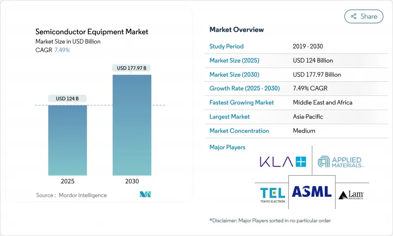
Robust fab construction, record equipment backlogs, and a wave of government incentives underpin this trajectory. Foundries are accelerating capacity at 2 nm and below, while Outsourced Semiconductor Assembly and Test (OSAT) players scale advanced-package lines to serve artificial-intelligence (AI) demand. Geopolitical efforts to achieve technological sovereignty are shaping capital-spending patterns, forcing tool vendors to juggle export controls in China with subsidy-fuelled opportunities in North America, Europe, and the Middle East. Equipment makers that bundle process breadth, software analytics, and service coverage are securing multi-year purchase commitments from the sector's largest investors.
Global Semiconductor Equipment Market Trends and Insights
Surging demand for advanced consumer electronics and smartphones
Smartphones, wearables, and mixed-reality devices keep adding logic, memory, and analog content that must be built at ever-smaller nodes, pushing foundries to accelerate capacity on 28 nm-7 nm lines. Advanced packaging that miniaturizes high-bandwidth functions without raising power budgets drove a sizable share of early-2025 revenue, triggering an upgrade wave in bumping, test, and lithography equipment. Heterogeneous-integration lines stacking chiplets vertically are expanding at double-digit rates, lifting shipments of flip-chip bonders and wafer-level inspection tools. Tool makers offering modular deposition chambers with rapid recipe switching are winning orders as consumer-product cycles tighten. Strong handset refresh rates across India and Southeast Asia keep mature-node tools running near full utilization, proving that resilient billings are achievable even during premium-device launches.
Rapid AI-, IoT- and edge-device node investments
Data-center operators seek chips that offer higher TOPS-per-watt, boosting procurement of extreme ultraviolet (EUV) scanners and atomic-layer deposition modules used at 3 nm and below. AI accelerator start-ups in the United States and Europe are signing capacity reservation agreements that tie multi-year HBM purchases to guaranteed access to leading-edge lithography, shifting demand risk from chip designers to equipment makers. Edge AI devices for factory automation and smart-city deployments accelerate 16 nm-12 nm demand, spurring fresh orders for 300 mm etch systems tailored to embedded non-volatile memory. Tool suppliers deploy AI in situ process-monitoring algorithms, shortening recipe-development cycles and improving chamber uptime. The self-reinforcing loop between AI workload growth and smarter tools bolsters the semiconductor equipment market well past 2030.
Extremely high CAPEX and long pay-back cycles
A single advanced-logic fab now costs well above USD 20 billion, making the customer base for leading-edge tools increasingly concentrated. Lengthy depreciation periods stretch procurement scrutiny, compelling toolmakers to demonstrate multi-node extendibility before purchase orders are released. Vendors respond with upgrade-ready platforms, modular vacuum geometries, and subscription-based process-control software that spreads cost over a tool's life span. Some IDMs delay capacity expansions, which defers installations and shifts revenue recognition to late project phases. Nevertheless, the relentless need for performance-per-watt keeps road maps intact, limiting the overall drag on the semiconductor equipment market.
Other drivers and restraints analyzed in the detailed report include:
- Government subsidy waves are boosting the tool CAPEX
- Transition to GAA and High-NA EUV necessitates new toolsets
- Specialty-material supply bottlenecks are delaying tool shipments
For complete list of drivers and restraints, kindly check the Table Of Contents.
Segment Analysis
Front-end wafer-processing instruments captured 83.7% of the semiconductor equipment market share in 2024, underscoring the central role of lithography, etch, and deposition in yield improvement. Within this segment, High-NA EUV scanners post a 21.1% CAGR to 2030 because they are indispensable for patterning 2 nm logic and 3-D DRAM structures; multi-system orders from fabs in Taiwan and New York already total several billion USD.
Backend complexity fuels innovations such as thermo-compression bonders with sub-2 µm alignment accuracy and fan-out wafer-level packaging that leverages front-end lithographic precision. Vendors that combine lithography optics, placement robotics, and high-frequency test modules into unified platforms are capturing a growing share of advanced-package budgets, extending lithography-grade investments further down the supply chain.
Foundries accounted for 52.2% of semiconductor equipment market revenue in 2024 as fabless chip firms concentrate orders on TSMC, Samsung Foundry, and GlobalFoundries. Mega-projects in Arizona, Dresden, and Kaohsiung each feature clusters of EUV scanners, multi-chamber etch stacks, and atomic-layer deposition tools configured for rapid recipe swaps, reflecting the foundry model's need to host diverse customer process flows. Strict uptime commitments drive bundled service contracts that now equal 25-30% of tool acquisition value, creating annuity streams for equipment suppliers.
OSAT houses emerge as the fastest-growing customer category at a 12.2% CAGR, propelled by 2.5-D and 3-D package architectures required for AI accelerators and automotive domain controllers. New capex lines include laser-drilling for through-silicon vias, high-density flip-chip bonders, and molded-underfill dispense systems. Integrated device manufacturers (IDMs) retain a sizeable but declining share as they pursue fab-lite strategies that outsource leading-edge logic while investing selectively in power, analog, and sensor lines.
Semiconductor Equipment Market is Segmented by Equipment Type (Front-End Equipment, and Back-End Equipment), Supply Chain Participant (IDM, Foundry, and OSAT), Wafer Size (300 Mm, 200 Mm, and <=150 Mm), Fab Technology Node (>=28 Nm, 16/14 Nm, and More), End-User Industry (Computing and Data-Center, Communications (5G, RF), and More), and Geography (North America, South America, Europe, Asia-Pacific, and Middle East and Africa).
Geography Analysis
Asia-Pacific retained 72.2% semiconductor equipment market share in 2024, powered by dense ecosystems in Taiwan, South Korea, and mainland China; Taiwan's foundry cluster alone ran above 90% utilization, sustaining EUV and metrology orders. South Korea intensified spending on 1-beta DRAM and gate-all-around logic, while China's drive for self-reliance lifted domestic etcher and deposition installations even under export-control pressure.
North America's renaissance stems from CHIPS Act grants; Albany NanoTech took delivery of the world's first High-NA EUV tool, creating a cornerstone for a domestic lithography ecosystem. Simultaneous investments by TSMC and Intel in Arizona form a corridor stretching from equipment assembly in Oregon to materials supply in Texas, re-balancing regional demand.
Europe sharpened its specialty-technology focus-automotive power devices, RF front-ends, and advanced sensors-using the European Chips Act to target a doubling of regional capacity by 2030; Saxony's dual 300 mm lines already combine logic, analog, and power processing.
The Middle East and Africa logged the fastest growth at 9.9% CAGR, fuelled by Saudi Arabia's USD 9 billion fab plan and UAE feasibility studies, which require turnkey tool-support contracts spanning training, refurbishment, and logistics. South America remains niche; Brazil is investing selectively in automotive and industrial chips that rely on mature-node 200 mm tools.
- Applied Materials Inc.
- ASML Holding NV
- Tokyo Electron Ltd.
- Lam Research Corp.
- KLA Corp.
- Screen Holdings Co. Ltd.
- Teradyne Inc.
- Hitachi High-Tech Corp.
- Veeco Instruments Inc.
- ASM International NV
- Canon Inc.
- Nikon Corp.
- Onto Innovation Inc.
- Nova Ltd.
- Advantest Corp.
- Hanmi Semiconductor Co. Ltd.
- Disco Corp.
- BESI (BE Semiconductor Industries)
- Kulicke & Soffa Industries Inc.
- FormFactor Inc.
- Plasma-Therm LLC
- SUSS MicroTec SE
- Kokusai Electric Corp.
- AMEC (Advanced Micro-Fabrication Equipment Inc.)
- Naura Technology Group Co. Ltd.
Additional Benefits:
- The market estimate (ME) sheet in Excel format
- 3 months of analyst support
TABLE OF CONTENTS
1 INTRODUCTION
- 1.1 Study Assumptions and Market Definition
- 1.2 Scope of the Study
2 RESEARCH METHODOLOGY
3 EXECUTIVE SUMMARY
4 MARKET LANDSCAPE
- 4.1 Market Overview
- 4.2 Market Drivers
- 4.2.1 Surging demand for advanced consumer electronics and smartphones
- 4.2.2 Rapid AI-, IoT- and edge-device node investments
- 4.2.3 Government subsidy waves (CHIPS, EU Chips Act, etc.) boosting tool CAPEX
- 4.2.4 Transition to GAA and High-NA EUV necessitating new toolsets
- 4.2.5 Sustainability mandates driving "green fab" retrofit tools
- 4.2.6 3D heterogeneous-integration packaging demand spike
- 4.3 Market Restraints
- 4.3.1 Extremely high CAPEX and long pay-back cycles
- 4.3.2 Specialty-material supply bottlenecks delaying tool shipments
- 4.3.3 Export-control restrictions on China-bound tools
- 4.3.4 Acute shortage of skilled field-service engineers
- 4.4 Value Chain Analysis
- 4.5 Regulatory Landscape
- 4.6 Technological Outlook
- 4.7 Porter's Five Forces Analysis
- 4.7.1 Bargaining Power of Suppliers
- 4.7.2 Bargaining Power of Buyers
- 4.7.3 Threat of New Entrants
- 4.7.4 Threat of Substitutes
- 4.7.5 Intensity of Competitive Rivalry
- 4.8 Impact of Macroeconomic Factors
5 MARKET SIZE AND GROWTH FORECASTS (VALUE)
- 5.1 By Equipment Type
- 5.1.1 Front-end Equipment
- 5.1.1.1 Lithography Equipment
- 5.1.1.2 Etch Equipment
- 5.1.1.3 Deposition Equipment
- 5.1.1.4 Metrology / Inspection Equipment
- 5.1.1.5 Cleaning Equipment
- 5.1.1.6 Photoresist Processing Equipment
- 5.1.1.7 Other Front-end Types
- 5.1.2 Back-end Equipment
- 5.1.2.1 Test Equipment
- 5.1.2.2 Assembly and Packaging Equipment
- 5.1.1 Front-end Equipment
- 5.2 By Supply-Chain Participant
- 5.2.1 IDM
- 5.2.2 Foundry
- 5.2.3 OSAT
- 5.3 By Wafer Size
- 5.3.1 300 mm
- 5.3.2 200 mm
- 5.3.3 <=150 mm
- 5.4 By Fab Technology Node
- 5.4.1 >=28 nm
- 5.4.2 16/14 nm
- 5.4.3 10/7 nm
- 5.4.4 5 nm and below
- 5.5 By End-user Industry
- 5.5.1 Computing and Data-Center
- 5.5.2 Communications (5G, RF)
- 5.5.3 Automotive and Mobility
- 5.5.4 Consumer Electronics
- 5.5.5 Industrial and Others
- 5.6 By Geography
- 5.6.1 North America
- 5.6.1.1 United States
- 5.6.1.2 Canada
- 5.6.1.3 Mexico
- 5.6.2 South America
- 5.6.2.1 Brazil
- 5.6.2.2 Argentina
- 5.6.2.3 Rest of South America
- 5.6.3 Europe
- 5.6.3.1 Germany
- 5.6.3.2 United Kingdom
- 5.6.3.3 France
- 5.6.3.4 Italy
- 5.6.3.5 Spain
- 5.6.3.6 Rest of Europe
- 5.6.4 Asia-Pacific
- 5.6.4.1 China
- 5.6.4.2 Japan
- 5.6.4.3 South Korea
- 5.6.4.4 India
- 5.6.4.5 Rest of Asia-Pacific
- 5.6.5 Middle East and Africa
- 5.6.5.1 Middle East
- 5.6.5.1.1 Saudi Arabia
- 5.6.5.1.2 United Arab Emirates
- 5.6.5.1.3 Turkey
- 5.6.5.1.4 Rest of Middle East
- 5.6.5.2 Africa
- 5.6.5.2.1 South Africa
- 5.6.5.2.2 Nigeria
- 5.6.5.2.3 Egypt
- 5.6.5.2.4 Rest of Africa
- 5.6.1 North America
6 COMPETITIVE LANDSCAPE
- 6.1 Market Concentration
- 6.2 Strategic Moves
- 6.3 Market Share Analysis
- 6.4 Company Profiles (includes Global-level Overview, Market-level Overview, Core Segments, Financials as available, Strategic Information, Market Rank/Share, Products and Services, Recent Developments)
- 6.4.1 Applied Materials Inc.
- 6.4.2 ASML Holding NV
- 6.4.3 Tokyo Electron Ltd.
- 6.4.4 Lam Research Corp.
- 6.4.5 KLA Corp.
- 6.4.6 Screen Holdings Co. Ltd.
- 6.4.7 Teradyne Inc.
- 6.4.8 Hitachi High-Tech Corp.
- 6.4.9 Veeco Instruments Inc.
- 6.4.10 ASM International NV
- 6.4.11 Canon Inc.
- 6.4.12 Nikon Corp.
- 6.4.13 Onto Innovation Inc.
- 6.4.14 Nova Ltd.
- 6.4.15 Advantest Corp.
- 6.4.16 Hanmi Semiconductor Co. Ltd.
- 6.4.17 Disco Corp.
- 6.4.18 BESI (BE Semiconductor Industries)
- 6.4.19 Kulicke & Soffa Industries Inc.
- 6.4.20 FormFactor Inc.
- 6.4.21 Plasma-Therm LLC
- 6.4.22 SUSS MicroTec SE
- 6.4.23 Kokusai Electric Corp.
- 6.4.24 AMEC (Advanced Micro-Fabrication Equipment Inc.)
- 6.4.25 Naura Technology Group Co. Ltd.
7 MARKET OPPORTUNITIES AND FUTURE OUTLOOK
- 7.1 White-space and Unmet-Need Assessment
