


|
시장보고서
상품코드
1940792
하이엔드 반도체 패키징 : 시장 점유율 분석, 업계 동향과 통계, 성장 예측(2026-2031년)High-End Semiconductor Packaging - Market Share Analysis, Industry Trends & Statistics, Growth Forecasts (2026 - 2031) |
||||||
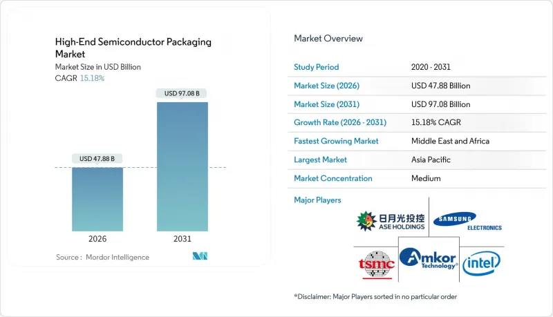
하이엔드 반도체 패키징 시장 규모는 2025년 415억 7,000만 달러에서 2026년 478억 8,000만 달러에 이를 것으로 예측됩니다.
2031년까지 예측은 970억 8,000만 달러에 달할 것으로 예상되며, 2026-2031년 연평균 복합 성장률(CAGR) 15.18%로 성장할 것으로 전망됩니다.
이종 통합에 대한 견조한 자본 유입, AI 가속기 수요의 급증, 기판 기술 혁신이 결합되어 강력한 성장 궤적을 뒷받침하고 있습니다. 파운더리의 수직적 통합은 기존 외주 조립 및 테스트(OSAT) 업체에 대한 경쟁 압력을 증가시키는 동시에 AI 칩 시장 출시 기간을 단축시킵니다. 스마트폰 및 자동차 시스템온칩(SoC) 공급업체들의 5nm 이하 미세화 전환은 팬아웃 및 실리콘 인터포저 플랫폼에 대한 점진적인 수요를 촉진할 것입니다. 미국의 CHIPS법에서 유럽의 APECS 허브에 이르기까지 지역 정책 인센티브는 공급망의 지역 구조를 재구성하고 다국적 기업의 선진 패키징 거점 분산화를 촉진하고 있습니다. 한편, 기판 부족과 열밀도 한계가 단기적인 생산능력 확대를 억제하는 한편, 이러한 병목현상을 완화할 수 있는 장비 제조업체와 재료 전문업체에 기회를 제공합니다.
세계 하이엔드 반도체 패키징 시장 동향 및 인사이트
AI/ML 가속기에 대한 수요 증가
하이퍼스케일 데이터센터 사업자들은 1,000W 이상의 연산 타일과 적층형 고대역폭 메모리를 통합한 멀티 다이 AI 프로세서로 전환하고 있으며, 이는 하이엔드 반도체 패키징 시장에서 고도의 열 관리 및 전력 공급에 대한 전례 없는 수요를 불러일으키고 있습니다. CoWoS(Chip-on-Wafer) 및 유사 인터포저 플랫폼의 생산 능력은 계속 타이트하게 유지되고 있으며, AI 제품 출시에 있어 패키징 리드타임이 매우 중요해지고 있습니다. 파운드리가 시스템 온 웨이퍼(System on Wafer) 개념을 활용하여 현재 GPU 대비 10배의 메모리 대역폭을 구현할 것을 약속하고 있어, 열 설계상의 문제를 더욱 심각하게 만들고 있습니다. 휨 제어, 마이크로 범프 신뢰성, 수냉식 기판을 마스터한 벤더는 하이퍼스케일러가 배포 일정을 달성할 수 있도록 가격 결정력을 확보할 수 있습니다. 그 결과, 패키징 능력은 현재 시스템 설계자들에 의해 AI 학습 비용과 시간을 결정하는 주요 요소로 간주되고 있습니다.
스마트폰용 첨단 공정으로 전환
프리미엄 스마트폰용 칩 제조업체들은 3nm 및 2nm 제조 노드로의 전환을 추진하고 있지만, 웨이퍼 비용의 상승으로 인해 비용 범위 내에서 성능을 구현하기 위해 팬아웃 웨이퍼 레벨 패키징과 임베디드 브리지 패키징의 병행적인 진화가 요구되고 있습니다. 요구되고 있습니다. 중국 스마트폰 제조업체들은 JCET의 6억 2,400만 달러 규모의 생산능력 확장 등 생산능력 인수를 배경으로 국내 OSAT 서비스 채택을 가속화하고, 가치사슬의 현지화와 지정학적 리스크 분산에 힘쓰고 있습니다. 노드 미세화를 통한 전력 예산 개선은 배터리 수명을 연장하고 기기에서 더 풍부한 AI 경험을 제공합니다. 그러나, 피치의 미세화에 따라 2µ&m 미만의 라인 앤 스페이스와 초박막 유전체를 갖춘 재배선층이 필요하게 됩니다. 고분자 화학 및 플라즈마 에칭 기술을 혁신하는 장비 공급업체는 이러한 미세 구조에서 높은 수율을 달성함으로써 경쟁 우위를 점하고 있습니다.
자본집약도 증가
업계의 자본집약도는 2015년 18%에서 2023년 30%로 상승하고, 차세대 패키징 라인은 EUV 리소그래피 지원 클린룸과 수억 달러 규모의 백엔드 장비가 필요하기 때문에 앞으로도 30% 이상을 유지할 것으로 예측됩니다. 중견 OSAT 기업들은 재정적 기반에 대한 압박에 직면하여 자금력이 있는 파운더리와의 통합 및 합작투자를 추진하고 있습니다. 설비투자액은 현재 전 공정 팹 지출과 비슷하며, 2033년까지 업계 전체가 4,600억 달러 이상에 달할 것으로 예측됩니다. ASMPT와 같은 주요 장비 제조업체조차도 2024년에 10%의 매출 감소를 보고하고 있으며, 이는 설비투자 집약적 사이클에 내재된 변동성을 강조하고 있습니다. 장기적으로는 지리적으로 분산된 사업 기반과 규모, 차별화된 공정 IP를 보유한 기업만이 연속적인 기술 노드에 대한 투자를 지속할 수 있을 것입니다.
부문 분석
2025년 하이엔드 반도체 패키지 시장에서 2.5D 인터포저가 가장 큰 점유율을 차지했습니다. 설계회사는 양산 시 검증된 수율과 제조성을 우선적으로 고려했기 때문입니다. 이 기술은 로직 다이와 HBM 다이를 융합하여 GPU와 FPGA에서 초당 수 테라비트 대역폭을 적당한 열 부하로 구현합니다. 반면, 3D 시스템온칩 분야는 규모는 작지만, 클라우드 및 엣지 디바이스의 AI 추론 이용 사례(로직과 메모리 스택을 함께 배치해야 함)를 배경으로 16.15%의 가장 빠른 CAGR을 나타낼 것으로 예측됩니다. 이러한 아키텍처가 성숙해짐에 따라 각 벤더들은 다이간 통신 프로토콜의 최적화를 통해 수직방향 신호 전송 지연을 줄이고 보급 확대를 가속화하고 있습니다.
인터포저에 대한 수요는 기판 공급업체의 수익 가시성을 높여주지만, ABF의 리드타임 리스크가 증가함에 따라 유리 및 실리콘 기반 인터포저에 대한 관심이 높아지고 있습니다. 한편, 3D 적층 메모리 패키지는 고대역폭 메모리 벤더의 대응 가능 기반을 확대하여 규모의 경제를 강화하고 있습니다. 인텔 EMIB와 같은 임베디드 브리지 기술은 완전한 인터포저의 복잡성 없이 55µm 미만의 다이간 피치를 구현하여 이종 통합을 위한 저비용의 도입 포인트를 제공합니다. 하이엔드 반도체 패키지 시장 규모에서 공정 제어의 혁신, 특히 하이브리드 본딩의 배치 정확도는 이 부문의 주요 차별화 요소로 남아있습니다.
플립칩 볼 그리드 어레이(FBGA)는 이미 확립된 제조거점과 검증된 신뢰성 지표로 인해 2025년 하이엔드 반도체 패키지 시장 점유율의 42.65%를 차지할 것으로 예측됩니다. 대체 플랫폼의 등장에도 불구하고 서버 CPU 및 GPU 타일의 지속적인 성장이 생산량을 뒷받침하고 있습니다. 패널 레벨 패키징(PLP)은 2031년까지 연평균 복합 성장률(CAGR) 16.32%로 성장할 전망입니다. 이는 더 큰 기판 형상으로 캐리어당 다이 수를 증가시켜 모바일 및 IoT용 SoC의 단가를 낮출 수 있기 때문입니다. 삼성의 파일럿 라인은 이미 600mm 유리 패널을 가공할 수 있으며, 300mm 웨이퍼의 처리 능력을 능가하여 기존 웨이퍼 레벨 패키징의 경제성을 위협하고 있습니다.
PLP의 보급은 에지 휨과 다이 배치 정확도 문제로 인해 제한을 받고 있으며, 벤더들은 진공 척과 비전 얼라인먼트 시스템을 개선해야 합니다. 시스템 인 패키지(SiP) 솔루션은 자동차용 레이더 모듈로 확대되고, 안테나와 전원 관리 IC를 통합하여 기판 면적을 줄입니다. 모바일 기기에서 웨이퍼 레벨 칩 스케일 패키지(WL-CSP)는 Z 방향의 높이 요구 사항과 비용 목표를 충족하고 수요의 모멘텀을 유지하고 있습니다. 하이엔드 반도체 패키지 시장이 발전함에 따라 제조업체들은 각 설계의 비용, 성능 및 신뢰성 요구 사항을 충족시키기 위해 혼합 플랫폼 팹 운영을 늘리고 있습니다.
하이엔드 반도체 패키징 보고서는 기술별(3D 시스템온칩, 3D 적층 메모리 등), 패키징 플랫폼별(플립칩 볼 그리드 어레이, 웨이퍼 레벨 칩 스케일 패키지 등), 디바이스 노드별(3nm 이하, 4-5nm 등), 최종사용자별(가전, 통신, 5G 인프라 등), 지역별로 분류됩니다. 최종사용자(가전, 통신 및 5G 인프라 등), 지역별로 분류되어 있습니다. 시장 예측은 금액(USD)으로 제공됩니다.
지역별 분석
아시아태평양은 대만의 파운드리 산업의 선도적 위치, 한국의 메모리 기술 전문성, 중국의 급속한 OSAT(위탁 조립, 테스트, 실장) 기반 구축을 배경으로 2025년 기준 하이엔드 반도체 패키징 시장의 58.85%를 차지할 것으로 예측됩니다. TSMC, ASE 테크놀로지, SPIL은 백엔드 라인을 프론트엔드 팹에 인접하게 배치하여 사이클 타임 단축과 물류 비용 절감을 실현하고 있습니다. 한편, 중국의 특혜 정책으로 국내 생태계가 육성되어 2030년까지 전 세계 패키징 설비 용량의 38%를 국내에서 충당한다는 목표를 세웠지만, 수출 관리 정책으로 인해 지정학적 불확실성이 가중되고 있습니다.
북미는 고부가가치 AI 및 방위산업 패키지에 집중하고 있으며, 520억 달러 규모의 CHIPS 법에 의한 자금 지원은 Amkor의 20억 달러 규모의 애리조나 공장과 인텔의 오하이오 주 패키징 메가 사이트를 지원하고 있습니다. 이 지역에는 장비 및 재료 공급업체가 밀집해 있어 차세대 기술을 위한 신속한 시제품 제작이 가능합니다. 유럽에서는 전략적 자율성을 추구하며 7억 3,000만 유로 규모의 APECS와 8억 3,000만 유로 규모의 FAMES라는 오픈 액세스 시제품 라인을 구축했습니다. 중소기업이 저렴한 가격으로 제조 물량을 확보할 수 있는 환경을 조성하고, 대륙 규모의 칩렛 생태계를 육성하고 있습니다.
중동 및 아프리카은 통신 인프라 구축과 반도체 허브에 투자하는 소버린 펀드에 힘입어 2031년까지 연평균 복합 성장률(CAGR) 18.05%를 나타낼 것으로 예측됩니다. 아랍에미리트 등 국가들은 엣지 AI 모듈에 대한 지역 수요를 겨냥해 세계 OSAT(위탁 조립, 테스트, 구현) 기업들과 제휴해 파일럿 라인에 공동 투자하고 있습니다. 남미는 아직 개발 단계에 있지만, 브라질의 가전제품 위탁 생산의 혜택을 받아 현지화된 테스트 및 마무리 서비스에 대한 수요가 증가하고 있습니다. 이 지리적 모자이크는 순수한 비용차이 추구에서 회복탄력성과 국가안보에 대한 고려로 전환하는 것을 강조하고 있습니다.
기타 특전:
- 엑셀 형식 시장 예측(ME) 시트
- 애널리스트의 3개월간 지원
자주 묻는 질문
목차
제1장 서론
제2장 조사 방법
제3장 주요 요약
제4장 시장 구도
제5장 시장 규모와 성장 예측
제6장 경쟁 구도
제7장 시장 기회와 향후 전망
LSH 26.03.10The high-end semiconductor packaging market size in 2026 is estimated at USD 47.88 billion, growing from 2025 value of USD 41.57 billion with 2031 projections showing USD 97.08 billion, growing at 15.18% CAGR over 2026-2031.

Robust capital flows toward heterogeneous integration, surging AI accelerator demand, and substrate innovations together reinforce a strong growth trajectory. Foundry vertical integration amplifies competitive pressure on traditional outsourced assembly and test (OSAT) vendors while improving time-to-market for AI chips. Sub-5 nm migration by smartphone and automotive system-on-chip (SoC) suppliers fuels incremental volume for fan-out and silicon interposer platforms. Regional policy incentives, from the U.S. CHIPS Act to Europe's APECS hub, are reshaping supply-chain geography, prompting multinational firms to diversify advanced packaging footprints. Meanwhile, substrate shortages and thermal-density limits temper near-term capacity ramps but simultaneously open opportunities for toolmakers and materials specialists that mitigate these bottlenecks.
Global High-End Semiconductor Packaging Market Trends and Insights
Rising Demand for AI/ML Accelerators
Hyperscale data-center operators pivot to multi-die AI processors that fuse >1,000 W compute tiles with stacked high-bandwidth memory, driving an unprecedented requirement for advanced thermal and power delivery inside the high-end semiconductor packaging market. Capacity for CoWoS and similar interposer platforms remains tight, elevating packaging lead-times to critical-path status for AI product launches. Foundries leveraging system-on-wafer concepts promise 10X memory bandwidth over current GPUs, further intensifying thermal engineering challenges. Vendors that master warpage control, micro-bump reliability, and liquid-coolable substrates gain pricing power as they enable hyperscalers to meet rollout schedules. Consequently, packaging capability is now viewed by system architects as a primary determinant of AI training cost and time.
Smartphone Migration to Advanced Nodes
Premium smartphone chipmakers are transitioning toward 3 nm and 2 nm production nodes, but rising wafer cost forces parallel advances in fan-out wafer-level and embedded bridge packaging to deliver performance within cost envelopes. Chinese handset brands accelerate adoption of domestic OSAT services following capacity acquisitions such as JCET's USD 624 million expansion, localizing value chains, and balancing geopolitical risk. Power-budget gains derived from finer nodes translate into longer battery life and richer on-device AI experiences; however, the tighter pitch requires redistribution layers with sub-2 µm line-and-space and ultra-thin dielectrics. Equipment suppliers innovating in polymer chemistries and plasma etch achieve a competitive advantage by enabling high volume yields at these geometries.
Escalating Capital Intensity
Industry capital intensity climbed from 18% in 2015 to 30% in 2023 and is expected to remain above 30% as next-generation packaging lines require EUV-litho-grade cleanrooms and back-end tools costing hundreds of millions of dollars. Mid-tier OSATs face balance-sheet stress, prompting consolidation or joint ventures with foundries wielding deep pockets. Equipment expenditures now rival front-end fab outlays, with projections exceeding USD 460 billion industry-wide by 2033. Even leading toolmakers such as ASMPT reported 10% revenue contraction in 2024, underscoring the volatility inherent in capex-heavy cycles. In the long term, only geographically diversified players with scale and differentiated process IP can fund successive technology nodes.
Other drivers and restraints analyzed in the detailed report include:
- Heterogeneous Integration Road-maps of IDMs/OSATs
- Growth of CoWoS-R for HPC Reticles
- Yield Management Complexity Beyond 5 nm
For complete list of drivers and restraints, kindly check the Table Of Contents.
Segment Analysis
2.5 D interposers captured the largest slice of the high-end semiconductor packaging market in 2025 as design houses prioritized proven yield and manufacturability at volume. The technology fuses logic and HBM dies with a moderate thermal penalty, supporting multi-terabit per second bandwidth in GPUs and FPGAs. By contrast, the 3D System-on-Chip segment, though smaller, is projected to clock the fastest 16.15% CAGR, underpinned by AI inference use cases in cloud and edge appliances that require co-located logic and memory stacks. As these architectures mature, vendors are optimizing die-to-die communication protocols to alleviate vertical signaling latency, accelerating broader adoption.
Interposer demand boosts revenue visibility for substrate suppliers, but mounting ABF lead-time risk has propelled interest in glass and silicon-based interposers. Meanwhile, 3D stacked-memory packages broaden the addressable base for high-bandwidth memory vendors, reinforcing scale economies. Embedded-bridge methods like Intel EMIB achieve die-to-die pitch <55 µm without full interposer complexity, offering a lower-cost entry point for heterogeneous integration. Within the high-end semiconductor packaging market size for this segment, process control innovations-especially hybrid bonding align accuracy-remain primary differentiators.
Flip-chip ball-grid-array held 42.65% of the high-end semiconductor packaging market share in 2025, thanks to an entrenched manufacturing base and well-documented reliability metrics. Continued growth in server CPUs and GPU tiles sustains volumes even as alternative platforms emerge. Panel-level packaging (PLP) rides a 16.32% CAGR through 2031 because larger substrate form factors permit more dies per carrier, lowering cost per unit for mobile and IoT SoCs. Samsung's pilot lines already process 600 mm glass panels, outpacing 300 mm wafer throughput and threatening traditional wafer-level economics.
PLP adoption is constrained by edge-warpage and die-placement accuracy challenges, compelling equipment vendors to refine vacuum-chuck and vision-alignment systems. System-in-Package solutions extend to automotive radar modules, integrating antennas and power management ICs to trim board area. In mobile devices, wafer-level chip-scale packages meet z-height mandates and cost goals, preserving demand momentum. As the high-end semiconductor packaging market evolves, manufacturers increasingly run mixed-platform fabs to align each design's cost, performance, and reliability envelope.
The High-End Semiconductor Packaging Report is Segmented by Technology (3D System-On-Chip, 3D Stacked Memory, and More), Packaging Platform (Flip-Chip Ball-Grid-Array, Wafer-Level Chip-Scale Package, and More), Device Node (Less Than or Equal To 3 Nm, 4-5 Nm, and More), End User (Consumer Electronics, Telecom and 5G Infrastructure, and More), and Geography. The Market Forecasts are Provided in Terms of Value (USD).
Geography Analysis
Asia-Pacific controlled 58.85% of the high-end semiconductor packaging market in 2025, anchored by Taiwan's foundry leadership, South Korea's memory expertise, and China's rapid OSAT build-out. TSMC, ASE Technology, and SPIL co-locate back-end lines next to front-end fabs, compressing cycle time and lowering logistic overhead. Simultaneously, Beijing's incentives foster a domestic ecosystem targeting 38% of global installed packaging capacity by 2030, though export-control policies add geopolitical uncertainty.
North America concentrates on high-value AI and defense-grade packages, buoyed by USD 52 billion CHIPS funding that subsidizes Amkor's USD 2 billion Arizona facility and Intel's Ohio packaging megasite. The region also houses a dense cluster of equipment and materials suppliers, allowing rapid prototyping for next-generation technologies. Europe pursues strategic autonomy through €730 million APECS and €830 million FAMES open-access pilot lines, giving SMEs affordable fabrication slots and seeding a continental chiplet ecosystem.
The Middle East and Africa chart an 18.05% CAGR through 2031, propelled by telecom infrastructure rollouts and sovereign funds investing in semiconductor hubs. Countries such as the United Arab Emirates partner with global OSATs to co-finance pilot lines, targeting regional demand for edge AI modules. South America remains nascent but benefits from consumer-electronics contract manufacturing in Brazil, generating incremental demand for localized test and finish services. The geographic mosaic underscores a shift from pure cost arbitrage toward resilience and national-security considerations.
- Advanced Semiconductor Engineering Inc. (ASE Technology Holding Co., Ltd.)
- Amkor Technology, Inc.
- Intel Corporation
- Taiwan Semiconductor Manufacturing Company Limited (TSMC)
- Samsung Electronics Co., Ltd.
- JCET Group Co., Ltd.
- Siliconware Precision Industries Co., Ltd. (SPIL)
- Powertech Technology Inc. (PTI)
- TongFu Microelectronics Co., Ltd.
- Fujitsu Limited
- Texas Instruments Incorporated
- United Microelectronics Corporation (UMC)
- STATS ChipPAC Pte Ltd.
- Hiksemi Microelectronics Co., Ltd.
- Nanium S.A. (Infineon Backend)
- Chip MOS Technologies Inc.
- Taiwan Advanced Packaging Corporation (TAPC)
- Unimicron Technology Corp.
- Shinko Electric Industries Co., Ltd.
- Kyocera Corporation (AVX)
Additional Benefits:
- The market estimate (ME) sheet in Excel format
- 3 months of analyst support
TABLE OF CONTENTS
1 INTRODUCTION
- 1.1 Study Assumptions and Market Definition
- 1.2 Scope of the Study
2 RESEARCH METHODOLOGY
3 EXECUTIVE SUMMARY
4 MARKET LANDSCAPE
- 4.1 Market Overview
- 4.2 Market Drivers
- 4.2.1 Rising demand for AI/ML accelerators
- 4.2.2 Smartphone migration to advanced nodes
- 4.2.3 Heterogeneous integration road-maps of IDMs/OSATs
- 4.2.4 Adoption of chip-lets for LEO satellite payloads
- 4.2.5 Growth of Chip-on-Wafer-on-Substrate (CoWoS-R) for HPC reticles
- 4.2.6 Government-funded 'More-than-Moore' pilot lines in Europe
- 4.3 Market Restraints
- 4.3.1 Escalating capital intensity
- 4.3.2 Yield management complexity beyond 5 nm
- 4.3.3 Sub-strate supply bottlenecks for organic interposers
- 4.3.4 Non-uniform thermal dissipation in 3D-SoC stacks
- 4.4 Industry Value Chain Analysis
- 4.5 Regulatory Landscape
- 4.6 Technological Outlook
- 4.7 Porter's Five Forces Analysis
- 4.7.1 Bargaining Power of Suppliers
- 4.7.2 Bargaining Power of Buyers
- 4.7.3 Threat of New Entrants
- 4.7.4 Threat of Substitutes
- 4.7.5 Degree of Competition
- 4.8 Assessment of Macroeconomic Impact
5 MARKET SIZE AND GROWTH FORECASTS (VALUE)
- 5.1 By Technology
- 5.1.1 3D System-on-Chip (3D-SoC)
- 5.1.2 3D Stacked Memory (HBM, HBM-PIM)
- 5.1.3 2.5D Interposers
- 5.1.4 Ultra-High-Density Fan-Out (UHD-FO)
- 5.1.5 Embedded Si Bridge / EMIB
- 5.2 By Packaging Platform
- 5.2.1 Flip-Chip Ball-Grid-Array (FC-BGA)
- 5.2.2 Wafer-Level Chip-Scale Package (WLCSP)
- 5.2.3 Panel-Level Packaging (PLP)
- 5.2.4 System-in-Package (SiP)
- 5.3 By Device Node
- 5.3.1 Less than or Equal to 3 nm
- 5.3.2 4-5 nm
- 5.3.3 6-7 nm
- 5.3.4 Greater than or Equal to 10 nm
- 5.4 By End User
- 5.4.1 Consumer Electronics
- 5.4.2 Telecom and 5G Infrastructure
- 5.4.3 Automotive and ADAS
- 5.4.4 Aerospace and Defense
- 5.4.5 Medical Devices
- 5.5 By Geography
- 5.5.1 North America
- 5.5.1.1 United States
- 5.5.1.2 Canada
- 5.5.1.3 Mexico
- 5.5.2 South America
- 5.5.2.1 Brazil
- 5.5.2.2 Argentina
- 5.5.2.3 Colombia
- 5.5.2.4 Rest of South America
- 5.5.3 Europe
- 5.5.3.1 United Kingdom
- 5.5.3.2 Germany
- 5.5.3.3 France
- 5.5.3.4 Italy
- 5.5.3.5 Spain
- 5.5.3.6 Rest of Europe
- 5.5.4 Asia-Pacific
- 5.5.4.1 China
- 5.5.4.2 Japan
- 5.5.4.3 South Korea
- 5.5.4.4 India
- 5.5.4.5 Rest of Asia-Pacific
- 5.5.5 Middle East and Africa
- 5.5.5.1 Middle East
- 5.5.5.1.1 Saudi Arabia
- 5.5.5.1.2 United Arab Emirates
- 5.5.5.1.3 Rest of Middle East
- 5.5.5.2 Africa
- 5.5.5.2.1 South Africa
- 5.5.5.2.2 Egypt
- 5.5.5.2.3 Rest of Africa
- 5.5.5.1 Middle East
- 5.5.1 North America
6 COMPETITIVE LANDSCAPE
- 6.1 Market Concentration
- 6.2 Strategic Moves
- 6.3 Market Share Analysis
- 6.4 Company Profiles (includes Global level Overview, Market level overview, Core Segments, Financials as available, Strategic Information, Market Rank/Share, Products and Services, Recent Developments)
- 6.4.1 Advanced Semiconductor Engineering Inc. (ASE Technology Holding Co., Ltd.)
- 6.4.2 Amkor Technology, Inc.
- 6.4.3 Intel Corporation
- 6.4.4 Taiwan Semiconductor Manufacturing Company Limited (TSMC)
- 6.4.5 Samsung Electronics Co., Ltd.
- 6.4.6 JCET Group Co., Ltd.
- 6.4.7 Siliconware Precision Industries Co., Ltd. (SPIL)
- 6.4.8 Powertech Technology Inc. (PTI)
- 6.4.9 TongFu Microelectronics Co., Ltd.
- 6.4.10 Fujitsu Limited
- 6.4.11 Texas Instruments Incorporated
- 6.4.12 United Microelectronics Corporation (UMC)
- 6.4.13 STATS ChipPAC Pte Ltd.
- 6.4.14 Hiksemi Microelectronics Co., Ltd.
- 6.4.15 Nanium S.A. (Infineon Backend)
- 6.4.16 Chip MOS Technologies Inc.
- 6.4.17 Taiwan Advanced Packaging Corporation (TAPC)
- 6.4.18 Unimicron Technology Corp.
- 6.4.19 Shinko Electric Industries Co., Ltd.
- 6.4.20 Kyocera Corporation (AVX)
7 MARKET OPPORTUNITIES AND FUTURE OUTLOOK
- 7.1 White-space and Unmet-Need Assessment
