

|
시장보고서
상품코드
2043993
SOI 실리콘 웨이퍼 : 시장 점유율 분석, 업계 동향 및 통계, 성장 예측(2026-2031년)SOI Silicon Wafer - Market Share Analysis, Industry Trends & Statistics, Growth Forecasts (2026 - 2031) |
||||||
 Mordor Intelligence
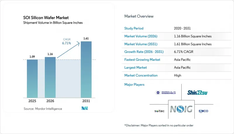
SOI 실리콘 웨이퍼 시장 규모는 2025년에 10억 9,000만 평방인치로 평가되었습니다. 2026년 11억 6,000만 평방인치에서 2031년까지 16억 1,000만 평방인치에 이를 것으로 예상되며, 예측 기간(2026-2031년) CAGR은 6.71%를 나타낼 전망입니다.
이러한 성장의 원동력은 SOI가 제공하는 유전체 절연과 백 바이어스 유연성을 필요로 하는 5G 무선 주파수 프론트엔드 모듈, 자동차 전원 관리 IC, 실리콘 포토닉스 상호연결에 있습니다. 300mm 기판 생산능력의 제약, 벌크 실리콘에 비해 여전히 2-3배 높은 비용, 소이테크의 'Smart Cut' 공정에 대한 지적재산권으로 인한 진입장벽이 성장을 저해하고 있지만, 파운드리 로드맵에서는 현재 28nm 이하 공정에서 벌크 CMOS보다 완전 공핍형 SOI 노드를 우선시하고 있기 때문에 보급이 저해되지는 않을 것입니다. 출하량은 아시아태평양이 주도하고 있지만, 미국 및 유럽의 정책 주도의 생산능력 증설로 인해 지역적 리스크 구도가 변화하고 있습니다. 따라서 각 디바이스 업체들은 SOI 실리콘 웨이퍼 시장에 대한 장기적인 공급 전략을 수립할 때, 성능 향상과 웨이퍼 공급 상황, 단위당 경제성을 동시에 고려하고 있습니다.
세계의 SOI 실리콘 웨이퍼 시장 동향 및 인사이트
5G RF 프론트엔드 모듈에서 FD-SOI의 급속한 확산
5G 및 초기 6G 스마트폰용 고주파 프론트엔드 모듈에서는 벌크 CMOS로는 대응하기 어려운 mm파 대역의 선형성 및 삽입 손실 목표를 달성하기 위해 RF-SOI 및 FD-SOI 기판에 대한 의존도가 높아지고 있습니다. GlobalFoundries의 9SW 플랫폼은 300mm RF-SOI에 스위치와 저잡음 증폭기를 통합하여 휴대폰 제조업체가 엄격한 전력 예산을 충족시키면서 기판 면적을 30% 줄일 수 있습니다. 타워세미컨덕터는 유사한 기술을 Wi-Fi 7로 확장하고, 브로드컴과 협력하여 6GHz 대역에서 0.4dB 이하의 삽입 손실을 실현했습니다. 2026년 초, 애플의 아이폰 17이 22FDX FD-SOI에서 제조된 퀄컴의 QTM565 안테나 모듈을 채택하여 대량 생산에 사용한 시연이 이루어졌습니다. VeriSilicon은 이미 1억 개 이상의 FD-SOI 연결용 칩을 출하했으며, 이는 SOI 실리콘 웨이퍼의 잠재적 시장을 확대하는 주류화 추세를 뒷받침하고 있습니다. 휴대폰 제조업체들이 6G 통합을 추진하면서 기판 공급업체들은 다이 면적 확대에 따른 수요 증가와 프리미엄 웨이퍼 가격의 혜택을 누리고 있습니다.
자동차 ADAS 및 전원 관리 IC의 SOI 통합 확대
자동차 제조업체들은 ISO 26262 기능 안전 표준을 준수하고 48V 전기 시스템에서 래치 업을 피하기 위해 배터리 관리 IC와 이미징 그레이더 트랜시버를 SOI로 전환하고 있습니다. 소이테크의 Power-SOI 제품군은 200V 동작을 지원하며, 배터리 모니터링 IC가 고가의 절연단 없이도 30셀 스트링을 모니터링할 수 있도록 함으로써 부품 비용을 15% 절감할 수 있습니다. 자동차 레이더 매출은 2030년까지 220억 달러에 달할 것으로 예상되며, 22nm FD-SOI 공정은 350GHz 이상의 동작 주파수를 실현하여 4D 레이더의 요구 사항을 충족합니다. STMicroelectronics와 NXP는 300mm Power-SOI 라인의 인증을 획득하여 양산 체제를 갖추었음을 알 수 있습니다. 전기자동차 생산량이 증가함에 따라 SOI 기반의 개별 전력 및 혼합 신호 프로세서가 표준 선택이 되고 있으며, SOI 실리콘 웨이퍼 시장의 장기적인 성장 전망을 높이고 있습니다.
300mm SOI 웨이퍼 생산에 대한 세계 생산 능력의 한계
세계적으로 300mm SOI의 생산량은 연간 300만장 미만으로 300mm 벌크 실리콘 총 공급량의 2% 미만에 불과합니다. 소이테크의 베르낭과 싱가포르 공장이 약 200만 장을 공급하고 있는 반면, 신에츠케미칼과 SUMCO공급량은 50만 장에 불과합니다. 옥메틱의 2026년 증설 계획은 300mm가 아닌 200mm 수요에 대응하기 위한 것으로, 2027년 하반기 세계 웨이퍼스의 미국 및 이탈리아 공장이 양산 체제에 돌입할 때까지 생산 능력의 공백이 남게 됩니다. 이러한 공급 부족으로 인해 파운드리 업체들은 몇 분기에 걸친 계약을 체결해야 하고, 기판 가격은 매년 한 자릿수 비율로 상승하고 있으며, 새로운 생산 라인이 가동될 때까지 SOI 실리콘 웨이퍼 시장의 단기적인 성장이 정체될 수 있습니다.
부문 분석
300mm 부문은 2025년 생산량의 47.74%를 차지하며 2031년까지 연평균 7.17%의 연평균 복합 성장률(CAGR)을 나타낼 것으로 예상됩니다. 예측 기간 동안 SOI 실리콘 웨이퍼 시장 규모의 주요 견인차 역할을 할 것으로 전망됩니다. GlobalFoundries, STMicroelectronics, Tower Semiconductor와 같은 파운드리 업체들은 300mm 장비에서 RF-SOI 및 FD-SOI 공정을 표준화하여 다이 비용을 절감하고, 이미 저결함 밀도에 최적화된 성숙한 툴 세트를 재사용하고 있습니다. -SOI 공정을 표준화하고 있습니다. 새로운 5G, Wi-Fi 7, 자동차 레이더의 설계가 200mm에서 300mm로 이동함에 따라 기판 수요가 가속화되어 SOI 실리콘 웨이퍼 시장을 더욱 촉진하고 있습니다.
그러나 자동차용 파워 SOI의 발전은 여전히 200mm 라인에 의존하고 있습니다. 이는 해당 팹들이 이미 감가상각을 완료하고 긴 모델 수명주기에 대응하는 인증을 이미 획득했기 때문입니다. 300mm Smart Cut 라인 1개당 1억 달러의 투자를 정당화할 만큼의 세계 수요가 발생하기 전까지는 공급업체들은 하이브리드 체제를 유지할 것으로 보입니다. 150mm 이하의 형태는 인증 주기가 10년 이상에 이르는 내방사선 항공우주용 전자기기에서 틈새 시장으로 중요한 위치를 차지하고 있습니다. 그 결과, 웨이퍼 직경의 구성은 양극화 현상이 지속되겠지만, SOI 실리콘 웨이퍼 시장의 수익 중심은 2031년까지 300mm 기판으로 계속 옮겨갈 것으로 예측됩니다.
"SOI 실리콘 웨이퍼 시장 보고서는 웨이퍼 직경(150mm 이하, 200mm, 300mm), 반도체 디바이스 유형(로직, 메모리, 아날로그, 디스크리트, 기타 디바이스 유형), 최종 사용자(가전, 산업용, 통신, 자동차, 기타 최종 사용자), 지역별로 분류되어 있습니다. 지역별로 분류되어 있습니다. 시장 예측은 수량(평방인치) 기준으로 제시됩니다.
지역별 분석
아시아태평양은 2025년 출하량의 83.22%를 차지했으며, 2031년까지 연평균 복합 성장률(CAGR) 7.22%로 물량 측면에서 선두를 유지할 것으로 예측됩니다. 대만의 파운더리가 지역 수요를 지원하는 한편, 일본의 Shin-Etsu Chemical과 SUMCO가 현지 기판 공급을 담당하고 있습니다. 중국은 상하이 심구이(Shanghai Simgui)에서 국내 200mm SOI 생산을 확대하고 있으며, 수입 의존도를 낮추기 위해 300mm 생산 능력을 조사했으며, 지역 SOI 웨이퍼 시장을 더욱 확대되고 있습니다.
북미에서는 2027년 GlobalWafers의 미주리 및 텍사스 공장이 가동되면 성장이 가속화될 것으로 예측됩니다. 이를 통해 안정적인 조달을 중시하는 자동차, 방산, 통신 분야 고객사에 국내 공급이 가능해졌습니다. 유럽도 비슷한 길을 걷고 있습니다. ST마이크로일렉트로닉스의 크롤에 위치한 300mm FD-SOI 공장과 EU 칩스법 자금 지원을 받은 GlobalWafers의 노바라 공장은 공급망 리스크를 줄이고 원산지 규정 준수를 필요로 하는 지역 OEM의 요구에 부응하는 것을 목표로 합니다. 공급망 리스크를 줄이고 원산지를 준수해야 하는 지역 OEM의 요구에 부응하고자 합니다. 이러한 움직임이 맞물려 세계 SOI 실리콘 웨이퍼 시장은 현재 아시아 중심의 기반에서 다변화되고 있습니다.
남미, 중동 및 아프리카는 파운드리 인프라 부족으로 인해 공급량이 극히 미미합니다. 이스라엘의 타워반도체는 현지 팹에서 세계에 RF-SOI 모듈을 공급하고 있으며, 중동에서도 일정한 존재감을 유지하고 있습니다. 각국 정부가 보조금과 국내 생산능력을 연계하는 가운데, 지역 다변화 추세는 앞으로도 지속될 것이며, SOI 실리콘 웨이퍼 시장 전체의 지정학적 리스크는 점차 감소할 것으로 예측됩니다.
기타 혜택
- 엑셀 형태 시장 예측(ME) 시트
- 3개월간 애널리스트 지원
자주 묻는 질문
목차
제1장 서론
제2장 조사 방법
제3장 주요 요약
제4장 시장 구도
제5장 시장 규모와 성장 예측
제6장 경쟁 구도
제7장 시장 기회와 향후 전망
KTH 26.05.29The SOI silicon wafer market size was 1.09 billion square inches in 2025 and is estimated to grow from 1.16 billion square inches in 2026 to reach 1.61 billion square inches by 2031, at a CAGR of 6.71% during the forecast period (2026-2031).
Momentum stems from 5G radio-frequency front-end modules, automotive power-management ICs, and silicon-photonics interconnects that demand the dielectric isolation and back-bias flexibility SOI provides. Capacity constraints on 300 mm substrates, a persistent 2-to-3-times cost premium over bulk silicon, and the intellectual-property moat around Soitec's Smart Cut process temper growth but do not derail adoption, because foundry roadmaps now favor fully depleted SOI nodes over bulk CMOS at 28 nm and below. Asia-Pacific dominates shipments, yet policy-driven capacity additions in the United States and Europe are reshaping geographic risk. Device makers therefore juggle performance gains against wafer availability and unit economics as they plan long-term supply strategies for the SOI silicon wafer market.
Global SOI Silicon Wafer Market Trends and Insights
Rapid Adoption of FD-SOI for 5G RF Front-End Modules
Radio-frequency front-end modules for 5G and early 6G smartphones increasingly rely on RF-SOI and FD-SOI substrates to satisfy linearity and insertion-loss targets at millimeter-wave frequencies, where bulk CMOS struggles. GlobalFoundries' 9SW platform integrates switches and low-noise amplifiers on 300 mm RF-SOI, enabling handset makers to shrink board area by 30% while meeting stringent power budgets. Tower Semiconductor extended similar technology to Wi-Fi 7, partnering with Broadcom to achieve sub-0.4 dB insertion loss at 6 GHz. High-volume validation arrived when Apple's iPhone 17 used Qualcomm's QTM565 antenna module fabricated on 22FDX FD-SOI in early 2026. VeriSilicon has already shipped more than 100 million FD-SOI connectivity chips, underscoring a mainstream shift that widens the addressable SOI silicon wafer market. As handset OEMs pursue 6G integration, substrate suppliers benefit from richer die-area requirements and premium wafer pricing.
Increasing Integration of SOI in Automotive ADAS and Power-Management ICs
Vehicle makers have migrated battery-management ICs and imaging-radar transceivers to SOI to meet ISO 26262 functional-safety standards and to avoid latch-up in 48-volt electrical systems. Soitec's Power-SOI family supports 200-volt operation, allowing battery-monitor ICs to supervise 30-cell strings without costly isolation stages, cutting bill-of-materials cost by 15%. Automotive radar revenue is on track to reach USD 22 billion by 2030, and 22 nm FD-SOI processes deliver transit frequencies above 350 GHz, aligning with 4D radar requirements. STMicroelectronics and NXP have qualified 300 mm Power-SOI lines, signaling volume readiness. As electric-vehicle production climbs, discrete power and mixed-signal processors built on SOI are becoming default choices, lifting the long-term growth outlook for the SOI silicon wafer market.
Limited Global Capacity for 300 mm SOI Wafer Production
Worldwide, 300 mm SOI output remains below 3 million wafers per year, less than 2% of the total 300 mm bulk-silicon supply. Soitec's Bernin and Singapore plants deliver roughly 2 million wafers, while Shin-Etsu and SUMCO contribute only 0.5 million. Okmetic's 2026 expansion addressed 200 mm demand rather than 300 mm, leaving a capacity gap until GlobalWafers' U.S. and Italian plants reach volume in late 2027. Scarcity forces foundries into multi-quarter commitments, raises substrate prices by single-digit percentages each year, and threatens to cap near-term growth for the SOI silicon wafer market until new lines come online.
Other drivers and restraints analyzed in the detailed report include:
- Government Incentives for Domestic 300 mm SOI Fabs in Asia and Europe
- Demand Surge from Silicon Photonics in Hyperscale Data Centers
- Higher Cost Premium Over Bulk Silicon Substrates
For complete list of drivers and restraints, kindly check the Table Of Contents.
Segment Analysis
The 300 mm segment accounted for 47.74% of 2025 volume and is projected to expand at a 7.17% CAGR to 2031, making it the primary volume driver for the SOI silicon wafer market size over the forecast horizon. Foundries including GlobalFoundries, STMicroelectronics, and Tower Semiconductor have standardized RF-SOI and FD-SOI processes on 300 mm equipment to capture die-cost savings and to reuse mature tool sets already optimized for low-defect density. As new 5G, Wi-Fi 7, and automotive radar designs transit from 200 mm to 300 mm flows, substrate demand accelerates, further lifting the SOI silicon wafer market.
Advances in automotive Power-SOI, however, still rely on 200 mm lines because those fabs are fully depreciated and already qualified for long model-year lifecycles. Until global demand justifies the USD 100 million investment per Smart Cut line at 300 mm, suppliers will keep a hybrid footprint. Sub-150 mm formats retain niche relevance in radiation-hardened aerospace electronics, where qualification cycles run a decade or longer. Consequently, the wafer-diameter mix will remain bifurcated, but the revenue center of the SOI silicon wafer market will continue to pivot toward 300 mm substrates through 2031.
The SOI Silicon Wafer Market Report is Segmented by Wafer Diameter (Up To 150mm, 200mm, and 300mm), Semiconductor Device Type (Logic, Memory, Analog, Discrete, and Other Device Types), End-User (Consumer Electronics, Industrial, Telecommunications, Automotive, and Other End-Users), and Geography. The Market Forecasts are Provided in Terms of Volume (Square Inches).
Geography Analysis
Asia-Pacific held 83.22% of 2025 shipments and is set to maintain volume leadership with a 7.22% CAGR through 2031. Taiwan's foundries anchor regional demand, while Japan's Shin-Etsu and SUMCO provide local substrate supply. China is ramping domestic 200 mm SOI at Shanghai Simgui and researching 300 mm capacity to reduce reliance on imports, further expanding the regional SOI silicon wafer market.
North America is poised for accelerated growth once GlobalWafers' Missouri and Texas plants come online in 2027, offering a domestic supply to automotive, defense, and telecom customers that prize secure sourcing. Europe follows a parallel path; STMicroelectronics' 300 mm FD-SOI fab in Crolles and GlobalWafers' Novara plant, supported by EU Chips Act funding, aim to mitigate supply-chain risk and meet the needs of regional OEMs that require origin compliance. Together, these developments diversify the global SOI silicon wafer market away from its current Asia-heavy base.
South America and the Middle East, and Africa account for marginal volumes, constrained by limited foundry infrastructure. Nonetheless, Israel's Tower Semiconductor does supply global RF-SOI modules from its local fabs, maintaining a modest Middle Eastern footprint. Regional diversification trends will continue as governments tie subsidies to domestic capacity, incrementally lowering geopolitical risk across the SOI silicon wafer market.
- Soitec SA
- Shin-Etsu Chemical Co., Ltd.
- GlobalWafers Co., Ltd.
- SUMCO Corporation
- SK Siltron Co., Ltd.
- Okmetic Oy
- Shanghai Simgui Technology Co., Ltd.
- Wafer Works Corporation
- Siltronic AG
- GlobalFoundries Inc.
- Taiwan Semiconductor Manufacturing Company Limited
- Samsung Electronics Co., Ltd.
- STMicroelectronics N.V.
- NXP Semiconductors N.V.
- Tower Semiconductor Ltd.
- United Microelectronics Corporation
- ON Semiconductor Corporation
- IQE plc
- Semiconductor Manufacturing International Corporation
- Advanced Micro Foundry Pte. Ltd.
Additional Benefits:
- The market estimate (ME) sheet in Excel format
- 3 months of analyst support
TABLE OF CONTENTS
1 INTRODUCTION
- 1.1 Study Assumptions and Market Definition
- 1.2 Scope of the Study
2 RESEARCH METHODOLOGY
3 EXECUTIVE SUMMARY
4 MARKET LANDSCAPE
- 4.1 Market Overview
- 4.2 Industry Value-Chain Analysis
- 4.3 Technological Outlook
- 4.4 Impact of Macroeconomic Factors on the Market
- 4.5 Porter's Five Forces Analysis
- 4.5.1 Bargaining Power of Suppliers
- 4.5.2 Bargaining Power of Buyers
- 4.5.3 Threat of New Entrants
- 4.5.4 Threat of Substitutes
- 4.5.5 Intensity of Competitive Rivalry
- 4.6 Market Drivers
- 4.6.1 Rapid Adoption of FD-SOI for 5G RF Front-end Modules
- 4.6.2 Increasing Integration of SOI in Automotive ADAS and Power Management ICs
- 4.6.3 Government Incentives for Domestic 300 mm SOI Fabs in Asia and Europe
- 4.6.4 Demand Surge from Silicon Photonics in Hyperscale Data Centers
- 4.6.5 Emerging Neuromorphic and Quantum Computing Control Chips on SOI Substrates
- 4.6.6 Transition Toward Mixed-Signal IoT Devices Requiring Ultra-Low-Leakage SOI Nodes
- 4.7 Market Restraints
- 4.7.1 Limited Global Capacity for 300 mm SOI Wafer Production
- 4.7.2 Higher Cost Premium Over Bulk Silicon Substrates
- 4.7.3 Intellectual-Property Concentration Around Smart Cut and Eltran Processes
- 4.7.4 Wafer Edge-Void Defects Causing Yield Losses in Advanced FD-SOI Nodes
5 MARKET SIZE AND GROWTH FORECASTS (VOLUME)
- 5.1 By Wafer Diameter
- 5.1.1 Up to 150 mm
- 5.1.2 200 mm
- 5.1.3 300 mm
- 5.2 By Semiconductor Device Type
- 5.2.1 Logic
- 5.2.2 Memory
- 5.2.3 Analog
- 5.2.4 Discrete
- 5.2.5 Other Semiconductor Device Types
- 5.3 By End-user
- 5.3.1 Consumer Electronics
- 5.3.1.1 Mobile and Smartphones
- 5.3.1.2 PCs and Servers
- 5.3.2 Industrial
- 5.3.3 Telecommunications
- 5.3.4 Automotive
- 5.3.5 Other End-user Applications
- 5.3.1 Consumer Electronics
- 5.4 By Geography
- 5.4.1 North America
- 5.4.1.1 United States
- 5.4.1.2 Canada
- 5.4.1.3 Mexico
- 5.4.2 Europe
- 5.4.2.1 Germany
- 5.4.2.2 United Kingdom
- 5.4.2.3 France
- 5.4.2.4 Rest of Europe
- 5.4.3 Asia-Pacific
- 5.4.3.1 China
- 5.4.3.2 Japan
- 5.4.3.3 India
- 5.4.3.4 South Korea
- 5.4.3.5 Taiwan
- 5.4.3.6 Rest of Asia-Pacific
- 5.4.4 South America
- 5.4.5 Middle East and Africa
- 5.4.1 North America
6 COMPETITIVE LANDSCAPE
- 6.1 Market Concentration
- 6.2 Strategic Moves
- 6.3 Market Share Analysis
- 6.4 Company Profiles (includes Global Level Overview, Market Level Overview, Core Segments, Financials as available, Strategic Information, Market Rank/Share, Products and Services, Recent Developments)
- 6.4.1 Soitec SA
- 6.4.2 Shin-Etsu Chemical Co., Ltd.
- 6.4.3 GlobalWafers Co., Ltd.
- 6.4.4 SUMCO Corporation
- 6.4.5 SK Siltron Co., Ltd.
- 6.4.6 Okmetic Oy
- 6.4.7 Shanghai Simgui Technology Co., Ltd.
- 6.4.8 Wafer Works Corporation
- 6.4.9 Siltronic AG
- 6.4.10 GlobalFoundries Inc.
- 6.4.11 Taiwan Semiconductor Manufacturing Company Limited
- 6.4.12 Samsung Electronics Co., Ltd.
- 6.4.13 STMicroelectronics N.V.
- 6.4.14 NXP Semiconductors N.V.
- 6.4.15 Tower Semiconductor Ltd.
- 6.4.16 United Microelectronics Corporation
- 6.4.17 ON Semiconductor Corporation
- 6.4.18 IQE plc
- 6.4.19 Semiconductor Manufacturing International Corporation
- 6.4.20 Advanced Micro Foundry Pte. Ltd.
7 MARKET OPPORTUNITIES AND FUTURE OUTLOOK
- 7.1 White-space and Unmet-need Assessment


