
|
시장보고서
상품코드
2062042
SOI(Silicon on Insulator) : 시장 점유율 분석, 업계 동향 및 통계, 성장 예측(2026-2031년)Silicon On Insulator - Market Share Analysis, Industry Trends & Statistics, Growth Forecasts (2026 - 2031) |
||||||
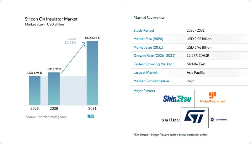
Mordor Intelligence에 의하면, SOI(Silicon on Insulator) 시장 규모는 2025년에 19억 6,000만 달러로 평가되었고, 예측 기간(2026-2031년) CAGR 12.27%로 확대될 전망이며, 2026년 22억 2,000만 달러에서 2031년에는 39억 6,000만 달러에 이를 것으로 추정되고 있습니다.
본 보고서는 SOI 플랫폼별(FD-SOI, PD-SOI, Power-SOI 및 기타 SOI 플랫폼), 웨이퍼 크기별(200mm 이하 및 201mm 이상), 기술별(본딩 SOI 등), 용도별(MEMS, 전원, 광통신 등), 최종 사용자 산업별(소비자 가전, 자동차, IT 및 통신 등), 지역별로 분류되어 있습니다. 시장 전망은 금액(달러) 기준으로 제시되어 있습니다.
세계 SOI(Silicon on Insulator) 시장 동향 및 분석
5G RF 프런트엔드 모듈에서의 FD-SOI 채택 확대
스마트폰의 무선 아키텍처에서는 캐리어 어그리게이션을 지원하기 위해 더 많은 파워 앰프, 스위치, 튜너가 통합되어 있습니다. FD-SOI는 고가의 기판을 사용하지 않으면서도 필요한 선형성과 고조파 억제 성능을 제공합니다. 다중 대역 지원 플래그십 모델이 출시된 2025년에는 RF-SOI 웨이퍼의 출하량이 크게 증가했습니다. 현재 파운드리 업체들은 무선 용도용 22nm FD-SOI 노드를 생산하고 있으며, 아날로그, 디지털, 파워 블록을 단일 다이 위에 통합함으로써 PCB의 실적를 줄이고 있습니다. 실시간 백바이어스를 통해 FD-SOI가 준수하는 3GPP Release 18 규격은 웨이퍼 수요를 더욱 견인하며, SOI(Silicon on Insulator) 시장의 확장을 뒷받침하고 있습니다. 또한, FD-SOI는 매시브 MIMO 무선 기술에도 점차 도입되고 있으며, 그 성장세는 휴대전화 단말기의 범위를 넘어 확장되고 있습니다.
고성능 및 저전력 엣지 AI 칩에 대한 수요 증가
자동차, 카메라, 웨어러블 기기에 탑재되는 엣지 추론 엔진은 테라 OP/초의 성능을 발휘하면서도 대기 시 전력 소비를 밀리와트 단위로 억제해야 합니다. FD-SOI의 초박형 바디는 누설 전류를 줄여주며, 0.4V까지의 저전압 동작을 지원하기 때문에 2025년에는 자동차용 AI SoC 분야에서 28nm FD-SOI 플랫폼의 채택이 확대될 전망입니다. 엔지니어들은 백 바이어스를 활용하여 -40°C에서 125°C에 이르는 온도 변동을 제어함으로써, 가드밴드 전압을 추가하지 않고도 안전 기준을 충족하고 있습니다. 이러한 접근 방식을 표준화함으로써 웨이퍼 생산량이 증가하고, 비용이 절감되며, 도입이 촉진되어 SOI(Silicon on Insulator) 시장이 확대될 것입니다.
300mm SOI 웨이퍼 생산 능력의 수급 불균형
2025년까지 양산 규모에 도달한 300mm 생산 라인은 단 하나뿐이며, 확장 일정은 2027년 하반기로 늦춰졌습니다. 각 파운드리 업체들은 벌크 실리콘에 비해 20-30% 높은 웨이퍼 비용에 직면해 있으며, 이로 인해 이익률이 압박을 받고 있어 대구경 웨이퍼로의 전환이 지연되고 있습니다. 일부 팹리스 기업들은 공급을 확보하기 위해 200mm 노드로 전환했으나, 이로 인해 생산량이 분산되고 비용 곡선의 평탄화가 지연되면서 단기적인 SOI 시장의 성장이 제한되고 있습니다. 대형 실리콘 원판 제조업체들은 두께 제어 기준의 강화와 300mm 공정에서 수소 주입 공정에 필요한 높은 자본 집약도 때문에 SOI에 대한 설비 투자에 있어 여전히 신중한 태도를 유지하고 있습니다. 단기적인 듀얼 소싱을 통한 대책은 엔지니어링 비용을 증가시킬 뿐이며, 부분적인 완화 효과에 그치고 있습니다.
부문별 분석
2025년 FD-SOI가 차지한 매출 점유율 54.21%는 SOI(Silicon on Insulator) 시장에서 가장 높은 비중을 차지했습니다. 이는 RF 트랜시버, 저전력 마이크로컨트롤러, 그리고 소비자용 웨어러블 기기에 대한 광범위한 채택에 힘입은 결과입니다. 각 OEM 업체들은 0.5V 미만의 전압으로 구동하면서도 차세대 무선 기기에 요구되는 이득 선형성과 노이즈 마진을 확보할 수 있다는 점에서 이 플랫폼을 선택했습니다. Power-SOI의 SOI(Silicon on Insulator) 시장 규모는 2026년부터 연평균 성장률(CAGR) 13.07%로 성장할 전망입니다.
공정 기술 측면에서 GlobalFoundries의 22nm FD-SOI 노드는 2025년 말까지 50건 이상의 자동차용 탭아웃을 기록하며, 꾸준한 설계 채택 추세를 입증하고 있습니다. ST마이크로일렉트로닉스와 삼성파운더리는 아날로그 및 혼합 신호 제품군에서 FD-SOI의 채택을 지속적으로 확대하고 있는 반면, 인피니온과 온세미컨덕터는 800V 구동계용 Power-SOI에 연구 개발을 집중하고 있습니다. 이 플랫폼의 분화로 인해 웨이퍼 공급업체는 특정 용도의 요구 사항에 맞추어 박스 및 핸들 층을 미세 조정할 수 있게 되었으며, 이는 SOI(Silicon on Insulator) 업계 전반에 걸쳐 가치 창출을 심화시키고 있습니다.
201mm 이상의 기판은 2025년 매출의 68.33%를 차지했으며, 생산량이 안정화되면 웨이퍼당 다이 수에 따른 규모의 경제 효과로 인해 비용을 약 3분의 1 수준으로 절감할 수 있음을 반영하고 있습니다. 대부분의 파운드리 업체들은 정부 지원 보조금 프로그램의 일환으로 유럽과 북미에 300mm SOI 생산 라인을 구축하고 있으며, 이로 인해 SOI(Silicon on Insulator) 시장의 이 부문이 더욱 공고해지고 있습니다. 그러나 300mm 웨이퍼의 스마트 컷팅에는 서브나노미터 수준의 두께 균일성이 요구됩니다. 따라서 수율 변동은 수백 개의 칩으로 급속히 파급되어, 발표된 생산 능력 확충 전략의 중요성을 여실히 보여주고 있습니다.
더 작은 직경의 웨이퍼는 MEMS 마이크로폰, 자이로 센서 및 집적 포토닉스 분야에서 여전히 활기를 띠고 있으며, 이러한 분야에서는 칩의 실적가 레티클 전체 면적보다 훨씬 작은 크기로 제한됩니다. Okmetic과 Wafer Works는 150mm 및 200mm 생산 라인에서 수익성 높은 틈새 시장을 유지하고 있으며, 더 짧은 사이클 타임을 활용해 스타트업 기업들과 함께 제품 개발을 지속적으로 진행하고 있습니다. 이러한 생산 능력은 설계자들이 300mm 웨이퍼 공급 부족에 대비해 위험을 분산할 때 안전판 역할을 하며, SOI(Silicon on Insulator) 시장 전체의 회복력을 유지하고 있습니다.
지역별 분석
2025년, 아시아태평양은 세계 매출의 46.83%를 차지했습니다. 이는 중국 내 파운드리 산업의 급속한 성장과 정밀 MEMS 제조 분야에서 일본이 지속적으로 유지해 온 우위에 힘입은 결과입니다. 대만과 한국은 최첨단 로직 및 메모리 기술로 시장의 기반을 다지고 있는 반면, 인도의 생산 연계형 인센티브 제도는 조립 및 테스트 분야에 대한 투자를 유치하여 웨이퍼 수요 증가로 이어지고 있습니다. 5G 기지국 및 엣지 AI 게이트웨이의 지역별 구축은 FD-SOI 및 Power-SOI 기판 수요를 더욱 확대시키고 있습니다.
북미에서는 정부 자금을 통한 팹 건설 프로젝트에 더해, 내방사선성을 중시하는 항공우주 및 방위 분야의 오랜 수요가 맞물려 있습니다. 인텔, 세계 파운드리, TSMC는 각각 2027년 양산 개시 시점에 300mm 특수 웨이퍼를 소비할 예정인 미국 내 시설 건설에 착수했습니다. 유럽도 이에 발맞추어 자동차 및 산업용 반도체를 대상으로 한 '칩스법'에 따른 430억 유로(484억 달러) 규모의 인센티브를 지원받고 있습니다. ST마이크로일렉트로닉스, 인피니온, NXP는 공급 리스크를 완화하기 위해 이미 현지 SOI 생산 능력을 로드맵에 반영했습니다.
중동은 가장 역동적인 신흥 시장으로, 정부계 펀드가 수십억 달러 규모의 자금을 광 인터커넥트 및 AI 가속기에 특화된 반도체 팹에 투자하고 있습니다. 아랍에미리트(UAE)와 사우디아라비아의 시범 사업에서는 SOI 포토닉스를 활용해 데이터센터의 에너지 소비 효율을 개선할 계획이며, 이는 해당 지역의 연평균 성장률(CAGR) 13.21%라는 전망을 뒷받침하고 있습니다. 남미와 아프리카는 생태계 발전 단계가 아직 초기 단계이지만, 브라질과 남아프리카공화국에서 진행 중인 시범 프로그램은 정책 체계가 성숙해짐에 따라 SOI(Silicon on Insulator) 시장에 향후 성장 여지가 있음을 시사하고 있습니다.
기타 혜택 :
- 엑셀 형식 시장 예측(ME) 시트
- 3개월간의 애널리스트 지원
자주 묻는 질문
목차
제1장 서론
제2장 조사 방법
제3장 주요 요약
제4장 시장 구도
제5장 시장 규모 및 성장 예측
제6장 경쟁 구도
제7장 시장 기회 및 향후 전망
AJY 26.06.22According to Mordor Intelligence, the silicon-on-insulator market size was valued at USD 1.96 billion in 2025 and is estimated to grow from USD 2.22 billion in 2026 to USD 3.96 billion by 2031, at a CAGR of 12.27% during the forecast period (2026-2031).

This report is Segmented by SOI Platform (FD-SOI, PD-SOI, Power-SOI, and Other SOI Platforms), Wafer Size (≤200 Mm, and ≥201 Mm), Technology (Bonding SOI, and More), Application (MEMS, Power Supplies, Optical Communication, and More), End-User Vertical (Consumer Electronics, Automotive, IT and Telecommunication, and More), and Geography. The Market Forecasts are Provided in Terms of Value (USD).
Global Silicon On Insulator Market Trends and Insights
Expanding Adoption of FD-SOI in 5G RF Front-End Modules
Smartphone radio architectures integrate more power amplifiers, switches, and tuners to support carrier aggregation, with FD-SOI providing required linearity and harmonic suppression without costlier substrates. RF-SOI wafer shipments grew significantly in 2025 as multi-band flagships launched. Foundries now produce 22 nm FD-SOI nodes for radio applications, combining analog, digital, and power blocks on a single die to reduce PCB footprints. 3GPP Release 18 standards, met by FD-SOI through real-time back-biasing, further drive wafer demand, boosting the silicon-on-insulator market. FD-SOI is also being adopted for massive-MIMO radios, expanding growth beyond handsets.
Growing Demand for High-Performance, Low-Power Edge AI Chips
Edge inference engines in vehicles, cameras, and wearables must meet milliwatt standby budgets while delivering tera-operations-per-second performance. FD-SOI's ultra-thin body reduces leakage and supports operation down to 0.4 V, driving automotive AI SoCs to adopt 28 nm FD-SOI platforms in 2025. Engineers use back-bias to manage temperature swings from -40 °C to 125 °C, meeting safety mandates without adding guard-band voltage. Standardizing this approach increases wafer volume, lowers costs, and boosts adoption, expanding the silicon-on-insulator market.
Supply-Demand Imbalance in 300 mm SOI Wafer Capacity
By 2025, only one high-volume 300 mm line reached scale, with expansions delayed until late 2027. Foundries face wafer costs 20%-30% higher than those for bulk silicon, squeezing margins and slowing migration to larger diameters. Some fabless customers shifted to 200 mm nodes to secure supply, but this diluted volumes and delayed cost curves, limiting near-term SOI market growth. Bulk-silicon giants remain cautious about SOI capex due to tighter thickness control and the higher capital intensity required for 300 mm hydrogen-implantation steps. Short-term dual-sourcing remedies raise engineering overhead, providing only partial relief.
Other drivers and restraints analyzed in the detailed report include:
- Governments' Strategic Semiconductor Sovereignty Initiatives
- Electric-Vehicle Powertrain Efficiency Improvements Using Power-SOI
- High Fabrication Cost Versus Bulk Silicon Alternatives
For complete list of drivers and restraints, kindly check the Table Of Contents.
Segment Analysis
The 54.21% revenue share held by FD-SOI in 2025 was the largest slice of the silicon-on-insulator market, buoyed by widespread deployment in RF transceivers, low-power microcontrollers, and consumer wearables. OEMs selected the platform for its ability to operate below 0.5 V while still delivering the gain linearity and noise margins demanded by next-generation radios. The silicon-on-insulator market size for Power-SOI is projected to grow at a 13.07% CAGR between 2026 and
At the process-technology level, GlobalFoundries' 22 nm FD-SOI node recorded more than 50 automotive tape-outs by year-end 2025, confirming robust design-win momentum. STMicroelectronics and Samsung Foundry continue to proliferate FD-SOI across analog and mixed-signal catalogs, whereas Infineon and ON Semiconductor channel R&D toward Power-SOI for 800 V drive trains. This platform bifurcation enables wafer suppliers to fine-tune box and handle layers for application-specific needs, deepening value capture across the silicon-on-insulator industry.
Substrates measuring 201 mm or more captured 68.33% of 2025 revenue, reflecting die-per-wafer leverage that cuts costs by roughly one-third once volume reaches steady state. Most foundries are positioning 300 mm SOI lines in Europe and North America under government-backed subsidy programs, further anchoring this segment of the silicon-on-insulator market. However, Smart Cut at 300 mm demands sub-nanometer thickness uniformity; yield excursions therefore ripple quickly across hundreds of dies, underscoring the strategic importance of announced capacity increases.
Smaller diameters retain vitality in MEMS microphones, gyro sensors, and integrated photonics, where die footprints cap out far below a full reticle. Okmetic and Wafer Works maintain profitable niches in 150 mm and 200 mm runs, using faster cycle times to iterate alongside start-ups. Such capacity provides a relief valve, as designers hedge against the tight supply of 300 mm blanks, preserving resilience across the broader silicon-on-insulator market.
Geography Analysis
Asia-Pacific commanded 46.83% of global revenue in 2025, anchored by China's indigenous foundry surge and Japan's enduring edge in precision MEMS fabrication. Taiwan and South Korea add depth through leading-edge logic and memory, while India's Production-Linked Incentive scheme is drawing assembly and test investments that will back-propagate wafer demand. Regional build-outs in 5G base stations and edge AI gateways further multiply consumption of FD-SOI and Power-SOI substrates.
North America combines sovereign-funded fab projects with long-standing aerospace and defense applications that value SOI for radiation hardness. Intel, GlobalFoundries, and TSMC have each broken ground on U.S. facilities slated to consume 300-mm specialty wafers when ramping begins in 2027. Europe follows closely, supported by EUR 43 billion (USD 48.4 billion) in Chips Act incentives that target automotive and industrial semiconductors. STMicroelectronics, Infineon, and NXP are already integrating localized SOI capacity into their roadmap to de-risk supply.
The Middle East represents the most dynamic frontier, with sovereign wealth funds allocating multibillion-dollar capital pools to semiconductor fabs focused on optical interconnects and AI accelerators. Pilot lines in the United Arab Emirates and Saudi Arabia plan to leverage SOI photonics to lower data-center energy intensity, reinforcing a 13.21% CAGR outlook for the region. South America and Africa are early in ecosystem development; nonetheless, pilot programs in Brazil and South Africa signal future upside for the silicon on insulator market as policy frameworks mature.
- Soitec SA
- Shin-Etsu Chemical Co., Ltd.
- GlobalWafers Co., Ltd.
- GlobalFoundries Inc.
- STMicroelectronics N.V.
- NXP Semiconductors N.V.
- Samsung Electronics Co., Ltd.
- Taiwan Semiconductor Manufacturing Company Limited
- Intel Corporation
- Siltronic AG
- SUMCO Corporation
- Okmetic Oyj
- Wafer Works Corporation
- NTT Advanced Technology Corporation
- China Silicon Corporation
- Skyworks Solutions, Inc.
- Infineon Technologies AG
- Murata Manufacturing Co., Ltd.
- Advanced Micro Devices, Inc.
- Analog Devices, Inc.
Additional Benefits:
- The market estimate (ME) sheet in Excel format
- 3 months of analyst support
TABLE OF CONTENTS
1 INTRODUCTION
- 1.1 Study Assumptions and Market Definition
- 1.2 Scope of the Study
2 RESEARCH METHODOLOGY
3 EXECUTIVE SUMMARY
4 MARKET LANDSCAPE
- 4.1 Market Overview
- 4.2 Market Drivers
- 4.2.1 Expanding Adoption of FD-SOI in 5G RF Front-End Modules
- 4.2.2 Growing Demand for High-Performance, Low-Power Edge AI Chips
- 4.2.3 Governments' Strategic Semiconductor Sovereignty Initiatives
- 4.2.4 Electric Vehicle Powertrain Efficiency Improvements Using Power-SOI
- 4.2.5 Rising Use of MEMS Sensors in Smart Industry 4.0 Applications
- 4.2.6 Surge in Optical Interconnects for Data Centers Leveraging SOI Photonics
- 4.3 Market Restraints
- 4.3.1 Supply-Demand Imbalance in 300 mm SOI Wafer Capacity
- 4.3.2 High Fabrication Cost Versus Bulk Silicon Alternatives
- 4.3.3 Complexity of Integrating SOI with Advanced Packaging Technologies
- 4.3.4 IP Ownership and Licensing Barriers in Smart Cut Process
- 4.4 Impact of Macroeconomic Factors on the Market
- 4.5 Industry Value Chain Analysis
- 4.6 Regulatory Landscape
- 4.7 Technological Outlook
- 4.8 Porter's Five Forces Analysis
- 4.8.1 Bargaining Power of Suppliers
- 4.8.2 Bargaining Power of Buyers
- 4.8.3 Threat of New Entrants
- 4.8.4 Threat of Substitutes
- 4.8.5 Intensity of Competitive Rivalry
5 MARKET SIZE AND GROWTH FORECASTS (VALUE)
- 5.1 By SOI Platform
- 5.1.1 Fully Depleted Silicon on Insulator (FD-SOI)
- 5.1.2 Partially Depleted Silicon on Insulator (PD-SOI)
- 5.1.3 Power-SOI
- 5.1.4 Other Types
- 5.2 By Wafer Size
- 5.2.1 Less Than or Equal To 200 mm
- 5.2.2 201 mm and Above
- 5.3 By Technology
- 5.3.1 Bonding SOI
- 5.3.2 Layer Transfer SOI
- 5.3.3 Smart Cut
- 5.4 By Application
- 5.4.1 MEMS
- 5.4.2 Power Supplies
- 5.4.3 Optical Communication
- 5.4.4 Image Sensing
- 5.4.5 Other Applications
- 5.5 By End-User Vertical
- 5.5.1 Consumer Electronics
- 5.5.2 Automotive
- 5.5.3 IT and Telecommunication
- 5.5.4 Aerospace and Defense
- 5.5.5 Industrial
- 5.5.6 Other End User Verticals
- 5.6 By Geography
- 5.6.1 North America
- 5.6.1.1 United States
- 5.6.1.2 Canada
- 5.6.1.3 Mexico
- 5.6.2 South America
- 5.6.2.1 Brazil
- 5.6.2.2 Argentina
- 5.6.2.3 Rest of South America
- 5.6.3 Europe
- 5.6.3.1 United Kingdom
- 5.6.3.2 Germany
- 5.6.3.3 France
- 5.6.3.4 Italy
- 5.6.3.5 Rest of Europe
- 5.6.4 Asia-Pacific
- 5.6.4.1 China
- 5.6.4.2 Japan
- 5.6.4.3 India
- 5.6.4.4 South Korea
- 5.6.4.5 Rest of Asia-Pacific
- 5.6.5 Middle East and Africa
- 5.6.5.1 Middle East
- 5.6.5.1.1 United Arab Emirates
- 5.6.5.1.2 Saudi Arabia
- 5.6.5.1.3 Rest of Middle East
- 5.6.5.2 Africa
- 5.6.5.2.1 South Africa
- 5.6.5.2.2 Egypt
- 5.6.5.2.3 Rest of Africa
- 5.6.5.1 Middle East
- 5.6.1 North America
6 COMPETITIVE LANDSCAPE
- 6.1 Market Concentration
- 6.2 Strategic Moves
- 6.3 Market Share Analysis
- 6.4 Company Profiles (includes Global Level Overview, Market Level Overview, Core Segments, Financials as available, Strategic Information, Market Rank/Share, Products and Services, Recent Developments)
- 6.4.1 Soitec SA
- 6.4.2 Shin-Etsu Chemical Co., Ltd.
- 6.4.3 GlobalWafers Co., Ltd.
- 6.4.4 GlobalFoundries Inc.
- 6.4.5 STMicroelectronics N.V.
- 6.4.6 NXP Semiconductors N.V.
- 6.4.7 Samsung Electronics Co., Ltd.
- 6.4.8 Taiwan Semiconductor Manufacturing Company Limited
- 6.4.9 Intel Corporation
- 6.4.10 Siltronic AG
- 6.4.11 SUMCO Corporation
- 6.4.12 Okmetic Oyj
- 6.4.13 Wafer Works Corporation
- 6.4.14 NTT Advanced Technology Corporation
- 6.4.15 China Silicon Corporation
- 6.4.16 Skyworks Solutions, Inc.
- 6.4.17 Infineon Technologies AG
- 6.4.18 Murata Manufacturing Co., Ltd.
- 6.4.19 Advanced Micro Devices, Inc.
- 6.4.20 Analog Devices, Inc.
7 MARKET OPPORTUNITIES AND FUTURE OUTLOOK
- 7.1 White-Space and Unmet-Need Assessment
