

|
시장보고서
상품코드
2044006
메모리 장치용 실리콘 웨이퍼 : 시장 점유율 분석, 업계 동향 및 통계, 성장 예측(2026-2031년)Silicon Wafer For Memory Devices - Market Share Analysis, Industry Trends & Statistics, Growth Forecasts (2026 - 2031) |
||||||
 Mordor Intelligence
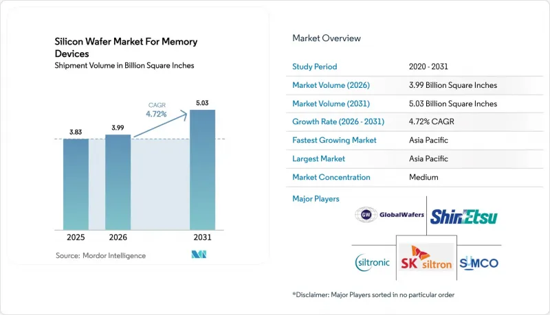
메모리 장치용 실리콘 웨이퍼 시장 규모는 2025년에 38억 3,000만 평방인치로 평가되었습니다. 2026년 39억 9,000만 평방인치에서 2031년까지 50억 3,000만 평방인치에 이를 것으로 예측되며, 2026년부터 2031년까지 연평균 복합 성장률(CAGR)은 4.72%를 나타낼 전망입니다.
고대역폭 메모리의 급속한 보급, 300mm 팹으로의 전환, 자동차 안전 기준의 강화로 인해 기판 사양이 재정의되고 있지만, 정부 보조금으로 인해 설비투자의 주기적 변동이 상쇄되고 있습니다. 하이브리드 본딩의 평탄도 요건을 충족하는 고품질 연마 웨이퍼에 대한 수요가 증가함에 따라 Tier 1 공급업체들의 협상력이 강화되고 있으며, 특수 SOI(절연막 상 실리콘) 기판은 자동차 레이더 및 5G RF 프론트엔드에서 수익성 높은 틈새 시장을 개척하고 있습니다. 미국의 'CHIPS and Science Act'와 유럽의 'Chips Act'에 기반한 공급망 지역화로 인해 단순한 가격 경쟁이 아닌 국가 안보를 축으로 한 경쟁관계에 있는 병렬적인 웨이퍼 생태계가 형성되고 있습니다. 에너지 소비 효율 규제 준수와 폴리실리콘 가격 변동에 대한 관심이 높아지면서 기판 업체들이 첨단 패키징 서비스로 사업을 다각화하고 있음에도 불구하고 여전히 비용 측면의 역풍으로 작용하고 있습니다.
메모리 장치용 실리콘 웨이퍼 시장 동향과 전망
300mm 팹으로의 전환 가속화
메모리 업체들은 200mm 라인을 폐지하고 웨이퍼당 다이 면적을 2.25배 확대하여 기가바이트당 기판 비용을 약 30% 절감할 수 있는 300mm 플랫폼에 자본을 투자하고 있습니다. TSMC의 쿠마모토 팹2는 자동차용 특수 D램을 위한 300mm 생산능력을 확보하고 있으며, Samsung Electronics와 SK하이닉스는 차세대 소재 개발을 가속화하기 위해 200mm 시설을 연구개발센터로 전환하고 있습니다. HBM3 E용 고급 노드는 300mm 기판에서만 경제성이 유지되는 실리콘 관통전극(TSV)에 의존하고 있습니다. 중국 및 대만의 중소 파운드리 업체들은 수출 규제 장벽을 극복하기 위해 재생 300mm 제조 장비를 적극적으로 도입하고 있으며, 이로 인해 도입 저변이 확대되어 장기적인 기판 수요를 뒷받침하고 있습니다. 이러한 추세에 따라 메모리 IDM 업체들은 로직과 DRAM을 같은 직경의 기판에 공존시킬 수 있게 되었으며, 이는 'Compute-in-Memory' 아키텍처의 효율화를 위한 핵심 요소입니다.
데이터센터의 AI 기반 메모리 수요 증가
현재 생성형 AI 클러스터는 DDR5에 비해 테라바이트당 40% 더 많은 웨이퍼 면적을 필요로 하는 HBM 스택을 채택하고 있습니다. SK하이닉스는 2025년 2분기에 12단 적층 HBM3 E를 출하하고 마이크론은 2026년 초에 36GB 스택으로 전환할 예정이며, 모두 미세 피치 구리 기둥 범프를 갖춘 300mm 베이스 웨이퍼를 채택하고 있습니다. 하이퍼스케일러들은 추론 워크로드용 GDDR7도 출시하고 있어, HBM용 초박형 웨이퍼와 GDDR7용 표준 웨이퍼를 동시에 공급할 수 있는 벤더에게 유리한 이중 수요 곡선이 형성되고 있습니다. SEMI는 AI 관련 DRAM이 2027년까지 전체 DRAM 웨이퍼 출하량의 28%에 달하고, 2024년 수준의 2배에 달할 것으로 전망하고 있습니다. GPU의 메모리 실적가 확대됨에 따라, DRAM 가격 하락 국면에서도 기판 수주가 견조하게 유지되고 있어 웨이퍼 공급업체의 수익 변동성을 완화하고 있습니다.
메모리 IDM을 통한 주기적 설비투자 절감
메모리 업체들은 DRAM 가격이 원가 이하로 떨어진 상황에서 2024년부터 2025년까지 120억 달러의 설비투자를 줄이고, 신공장 가동을 연기하는 한편, 웨이퍼 조달을 억제했습니다. 삼성은 평택 P4 공장 증설을 연기했고, 마이크론은 아이다호주와 싱가포르의 설비 도입을 연기했습니다. 웨이퍼의 생산 리드타임이 12-18개월인 점을 감안할 때, 갑작스러운 주문 취소는 기판 공급업체에 재고 과잉을 초래하여 수익률을 최대 300bp까지 떨어뜨리는 요인이 될 수 있습니다. Take or Pay 계약은 리스크를 줄일 수 있지만, 경기 침체기에는 IDM 업체들이 이를 거부하는 경향이 있어 시장 변동성이 장기화되는 경향이 있습니다.
부문 분석
메모리 장치용 실리콘 웨이퍼 시장에서 300mm 슬라이스는 2025년 수량 기준으로 85.73%의 점유율을 차지했으며, 이 부문은 2031년까지 연평균 5.11%의 연평균 복합 성장률(CAGR)을 나타낼 것으로 예측됩니다. 이러한 압도적인 점유율은 메모리 장치용 실리콘 웨이퍼 시장 규모가 직경 기준에서 상당히 크다는 것을 의미하며, 공급업체들이 초평탄화 연마 및 저결함 밀도화에 집중하고 있다는 것을 의미합니다. 10nm 이하 DRAM 노드용 극자외선(EUV) 리소그래피는 총 두께 편차를 0.2µm 이하로 유지해야 하지만, 이 기준을 충족하는 업체는 극소수에 불과해 진입장벽이 높습니다. 범용 200mm 웨이퍼는 기존 자동차용 파워 IC에서 여전히 수요가 있지만, 성장률은 2.8%에 불과하며, 재생 300mm 장비가 중국 및 동남아시아에 보급됨에 따라 감소 추세에 있는 것으로 나타났습니다. 150mm 미만의 웨이퍼는 MEMS의 틈새 시장에서 살아남고 있지만, 그 총 점유율은 1.3% 미만으로 주류 메모리 제조업체에게는 전략적으로 무의미한 존재가 되었습니다.
설비 상각 측면에서는 300mm 라인이 유리합니다. 왜냐하면 로트당 다이 표면적이 200mm 라인의 2.25배가 되는 반면, 인건비나 광열비가 비례적으로 증가하는 것은 아니기 때문입니다. TSMC가 구마모토 제2공장을 특수 D램 전용으로 전용한 것은 프리미엄급 300mm 생산능력을 놓고 메모리와 로직이 현재 정면으로 경쟁하고 있음을 보여줍니다. 그 결과, 2025년 체결된 장기 300mm 웨이퍼 계약 가격은 8-12% 상승했습니다. 신규 공장 건설에 5억 달러 이상의 비용이 들기 때문에 소규모 공급업체들은 철수하거나 합작회사를 설립하는 방법을 택하고 있습니다. 과점기업들은 규모의 경제를 활용하여 TSV(Through-Silicon Via) 지원 기판에 투자하여 미래 3D DRAM의 기회를 확보하고 있습니다.
"메모리 장치용 실리콘 웨이퍼 시장 보고서는 웨이퍼 직경(150mm 이하, 200mm, 300mm), 웨이퍼 유형(프라임 폴리싱, 에피택셜, SOI(절연막 상 실리콘), 특수 실리콘), 최종 사용자(소비자용 전자기기, 산업용, 통신, 기타), 지역(북미, 유럽, 아시아태평양, 기타)으로 분류되어 있습니다. 지역(북미, 유럽, 아시아태평양, 기타)으로 분류되어 있습니다. 시장 예측은 수량(평방인치) 기준으로 제공됩니다.
지역별 분석
아시아태평양은 2025년 생산량의 83.19%를 차지하며 메모리 장치용 실리콘 웨이퍼 시장을 독점했으며, 2031년까지 연평균 5.16% 성장할 것으로 예측됩니다. 한국의 평택과 이천에 위치한 수직 통합형 단지는 기판 리드 타임을 18개월에서 12개월로 단축하여 귀중한 수율 피드백 루프를 생성하고 있습니다. 대만 생태계는 TSMC-소니-덴소의 쿠마모토 합작 투자로 혜택을 받고 있으며, 이 사업을 통해 4,760억 엔(32억 달러)에 달하는 일본 보조금을 활용하여 DRAM 웨이퍼의 일부를 현지에서 생산하고 있습니다. 상하이 Simgui와 GRINM이 주도하는 중국의 아태지역 18% 점유율은 여전히 수입 폴리실리콘과 결정 인출 장비에 의존하고 있어 수출 규제로 인한 혼란의 가능성을 남기고 있습니다.
북미는 CHIPS 법의 보조금에 힘입어 2025년 생산량의 9%를 차지했습니다. 세계 웨이퍼의 샤먼 공장은 2028년까지 연간 120만 장의 300mm 웨이퍼를 생산할 계획이며, 이를 통해 미국의 수입 의존도를 낮출 수 있을 것으로 예측됩니다. 유럽의 점유율은 4%이지만, 인피니언과 ST마이크로일렉트로닉스의 확장을 지원하는 'CHIPS법'에 따른 430억 유로(460억 달러)의 인센티브 덕분에 4.3%의 속도로 소폭 성장하고 있습니다. 그럼에도 불구하고 공급 체제가 분산되어 있고, 실트로닉이 독일과 싱가포르에 걸쳐 있어 규모의 경제에 따른 비용 우위가 제한되어 있습니다. 남미, 중동 및 아프리카의 총 점유율은 여전히 1% 미만에 불과하며, 자국 내 메모리 제조 공장이 없고 막대한 설비투자라는 높은 진입장벽에 직면해 있습니다.
따라서 메모리 장치용 실리콘 웨이퍼 시장은 동아시아의 메가팹, 북미의 자체 생산능력, 유럽의 중규모 전문 생산라인의 세 가지 제조 거점으로 집약되고 있습니다. 정책 입안자들은 지역의 회복탄력성 강화를 추진하고 있지만, 원자재 집중과 제조 장비에 대한 의존도가 높아 진정한 자급자족을 실현하는 데는 몇 년이 더 걸릴 것으로 예측됩니다. 공급업체에게 이러한 지역적 구성은 점점 더 지역화되는 물류 네트워크에서 적시 납품을 보장하는 동시에 다양한 컴플라이언스 체제를 동시에 충족시켜야 한다는 것을 의미합니다.
기타 혜택 :
- 엑셀 형식 시장 예측(ME) 시트
- 3개월간 애널리스트 지원
자주 묻는 질문
목차
제1장 서론
제2장 조사 방법
제3장 주요 요약
제4장 시장 구도
제5장 시장 규모와 성장 예측
제6장 경쟁 구도
제7장 시장 기회와 향후 전망
KTH 26.05.29The silicon wafer market for memory devices market size was valued at 3.83 billion square inches in 2025 and estimated to grow from 3.99 billion square inches in 2026 to reach 5.03 billion square inches by 2031, at a CAGR of 4.72% during 2026-2031.
Rapid adoption of high-bandwidth memory, migration to 300 mm fabs, and tighter automotive safety requirements are reshaping substrate specifications, while government subsidies counterbalance cyclical capital-expenditure swings. Rising demand for prime polished wafers that meet hybrid-bonding flatness targets is deepening the bargaining power of tier-one suppliers, yet specialty silicon-on-insulator (SOI) substrates are carving a profitable niche in automotive radar and 5 G RF front-ends. Regionalization of supply chains under the US CHIPS and Science Act and the European Chips Act is creating parallel wafer ecosystems that compete on sovereign security rather than just price. Intensifying focus on energy-intensity compliance and polysilicon price volatility remains a cost headwind for substrate vendors even as they diversify into advanced-packaging services.
Insights and Trends of Silicon Wafer Market For Memory Devices
Accelerating Transition to 300 mm Fabs
Memory manufacturers are decommissioning 200 mm lines and pouring capital into 300 mm platforms that generate 2.25X more die area per wafer, slicing per-gigabyte substrate cost by roughly 30%. TSMC's Kumamoto Fab 2 earmarks 300 mm capacity for specialty DRAM aimed at automotive clients, and Samsung plus SK Hynix are repurposing 200 mm facilities into R&D centers to speed next-generation materials work. Advanced nodes for HBM3 E rely on through-silicon vias that remain economical only on 300 mm substrates. Smaller foundries in China and Taiwan are snapping up refurbished 300 mm toolsets to leapfrog export-control hurdles, widening the installed base and underpinning long-term substrate demand. The trend also lets memory IDMs co-locate logic and DRAM on the same diameter, an efficiency play for compute-in-memory architectures.
Expansion of AI-Driven Memory Demand in Data Centers
Generative-AI clusters now absorb HBM stacks that need 40% more wafer area per terabyte than DDR5. SK hynix shipped 12-high HBM3 E in 2Q 2025 and Micron moved to 36 GB stacks in early 2026, both based on 300 mm base wafers featuring fine-pitch copper pillar bumps. Hyperscalers also roll out GDDR7 for inference workloads, creating a dual-track demand curve that rewards wafer vendors who can supply ultra-flat substrates for HBM alongside standard wafers for GDDR7. SEMI projects AI-tied DRAM will hit 28% of total DRAM wafer starts by 2027, double 2024 levels. As GPU memory footprints expand, substrate orders remain resilient even during DRAM pricing dips, cushioning revenue swings for wafer suppliers.
Cyclical Cap-Ex Cuts by Memory IDMs
Memory producers slashed capital expenditure by USD 12 billion in 2024-2025 amid sub-cash-cost DRAM pricing, postponing new fab ramps and throttling wafer procurement. Samsung deferred its Pyeongtaek P4 expansion, and Micron delayed equipment installs in Idaho and Singapore. Given a 12-18-month wafer production lead time, abrupt order cancellations saddle substrate vendors with excess inventory, eroding margins by up to 300 basis points. Take-or-pay contracts could mitigate risk, but IDMs resist during downturns, prolonging volatility.
Other drivers and restraints analyzed in the detailed report include:
- Growing Automotive Memory for ADAS and EV Platforms
- Commercialization of 3 D DRAM/NRAM Stacks
- Supply Bottlenecks in Polysilicon Feedstock
For complete list of drivers and restraints, kindly check the Table Of Contents.
Segment Analysis
The 300 mm slice of the silicon wafer market for memory devices commanded 85.73% volume in 2025, and the segment is set to grow at 5.11% CAGR through 2031. That dominance translates into a substantial silicon wafer market size for memory devices at the diameter level, reinforcing supplier focus on ultra-flat polishing and low defect densities. Extreme ultraviolet lithography for sub-10 nm DRAM nodes imposes a total-thickness variation of less than 0.2 µm, a bar that only a few vendors can meet, reinforcing barriers to entry. Commodity 200 mm wafers retain traction for legacy automotive power ICs, yet a mere 2.8% growth rate flags a sunset trajectory as refurbished 300 mm toolsets permeate China and Southeast Asia. Wafers under 150 mm persist in MEMS niches, but their combined share is less than 1.3%, rendering them strategically irrelevant for mainstream memory producers.
Equipment amortization favors 300 mm lines because a single lot delivers 2.25X the die surface area of 200 mm lines without proportionally higher labor or utility costs. TSMC's choice to dedicate Kumamoto Fab 2 to specialty DRAM shows memory is now vying head-to-head with logic for premium 300 mm capacity. As a result, long-term 300 mm wafer contracts signed in 2025 rose in price by 8-12%. Smaller suppliers either exit or form joint ventures given greenfield fabs cost upward of USD 500 million. Oligopolists leverage scale to invest in through-silicon via ready substrates, locking in future 3 D DRAM opportunities.
The Silicon Wafer Market for Memory Devices Report is Segmented by Wafer Diameter (Up To 150mm, 200mm, and 300mm), Wafer Type (Prime Polished, Epitaxial, Silicon-On-Insulator, and Specialty Silicon), End-User (Consumer Electronics, Industrial, Telecommunications, and More), and Geography (North America, Europe, Asia-Pacific, and More). The Market Forecasts are Provided in Terms of Volume (Square Inches).
Geography Analysis
Asia-Pacific dominated the silicon wafer market for memory devices with 83.19% production volume in 2025, growing at 5.16% CAGR to 2031. South Korea's vertically integrated complexes in Pyeongtaek and Icheon shave substrate lead times from 18 to 12 months, yielding valuable yield-feedback loops. Taiwan's ecosystem benefits from TSMC-Sony-Denso's Kumamoto venture, which channels Japanese subsidies worth JPY 476 billion (USD 3.2 billion) to localize DRAM wafers. China's 18% slice within Asia-Pacific, led by Shanghai Simgui and GRINM, is still reliant on imported polysilicon and crystal-pulling tools, keeping the door open for export-control disruptions.
North America accounted for 9% of 2025 volume, lifted by CHIPS Act grants. GlobalWafers' Sherman plant will add 1.2 million 300 mm wafers annually by 2028, reducing U.S. dependence on imports. Europe's 4% share inches ahead at a 4.3% pace thanks to EUR 43 billion (USD 46 billion) in Chips Act incentives supporting Infineon and STMicroelectronics expansions. Still, supply remains fragmented, with Siltronic spanning Germany and Singapore, limiting scale-related cost advantages. South America and the Middle East and Africa together remain below 1%, lacking indigenous memory fabs and facing steep capital-barrier hurdles.
The silicon wafer market for memory devices therefore clusters around three manufacturing zones, East Asia mega-fabs, North American sovereign capacity, and Europe's mid-scale specialty lines. Policymakers push for local resilience, but raw-material concentration and tooling dependencies mean genuine self-sufficiency is years away. For suppliers, this geography mix implies juggling multiple compliance regimes while ensuring just-in-time delivery over an increasingly regionalized logistics map.
- Shin-Etsu Chemical Co., Ltd.
- SUMCO Corporation
- GlobalWafers Co., Ltd.
- Siltronic AG
- SK Siltron Co., Ltd.
- Soitec SA
- Okmetic Oy
- Wafer Works Corporation
- Zing Semiconductor Corporation
- Topsil Semiconductor Materials A/S
- Silicon Materials Inc.
- GCL-Advanced Material Co., Ltd.
- Shanghai Simgui Technology Co., Ltd.
- GRINM Semiconductor Materials Co., Ltd.
- Zhejiang Jinruihong (QL Electronics)
- Kinik Company
- Poshing Microelectronics Ltd.
- Win Win Precision Technology Co., Ltd.
- Nan Ya Photonics Inc.
Additional Benefits:
- The market estimate (ME) sheet in Excel format
- 3 months of analyst support
TABLE OF CONTENTS
1 INTRODUCTION
- 1.1 Study Assumptions and Market Definition
- 1.2 Scope of the Study
2 RESEARCH METHODOLOGY
3 EXECUTIVE SUMMARY
4 MARKET LANDSCAPE
- 4.1 Market Overview
- 4.2 Industry Value Chain Analysis
- 4.3 Technology Analysis
- 4.4 Regulatory Landscape
- 4.5 Impact of Macroeconomic Factors on the Market
- 4.6 Market Drivers
- 4.6.1 Accelerating Transition to 300 mm Fabs
- 4.6.2 Expansion of AI-Driven Memory Demand in Data Centers
- 4.6.3 Growing Automotive Memory for ADAS and EV Platforms
- 4.6.4 Commercialization of 3D DRAM/NRAM Stacks
- 4.6.5 In-line Laser Anneal Boosting Wafer Yields
- 4.6.6 Government CHIPS Incentives for Local Wafer Ecosystems
- 4.7 Market Restraints
- 4.7.1 Cyclical Cap-Ex Cuts by Memory IDMs
- 4.7.2 Supply Bottlenecks in Polysilicon Feedstock
- 4.7.3 Escalating Energy-Intensity Compliance Costs
- 4.7.4 Delayed Qualification of 450 mm Toolsets
- 4.8 Technological Outlook
- 4.9 Porter's Five Forces Analysis
- 4.9.1 Bargaining Power of Suppliers
- 4.9.2 Bargaining Power of Buyers
- 4.9.3 Threat of New Entrants
- 4.9.4 Threat of Substitutes
- 4.9.5 Intensity of Competitive Rivalry
5 MARKET SIZE AND GROWTH FORECASTS (VOLUME)
- 5.1 By Wafer Diameter
- 5.1.1 Up to 150 mm
- 5.1.2 200 mm
- 5.1.3 300 mm
- 5.2 By Wafer Type
- 5.2.1 Prime Polished
- 5.2.2 Epitaxial
- 5.2.3 Silicon-on-Insulator (SOI)
- 5.2.4 Specialty Silicon (High-Resistivity, Power, Sensor-Grade)
- 5.3 By End-user
- 5.3.1 Consumer Electronics
- 5.3.1.1 Mobile and Smartphones
- 5.3.1.2 PCs and Servers
- 5.3.2 Industrial
- 5.3.3 Telecommunications
- 5.3.4 Automotive
- 5.3.5 Other End-user Applications
- 5.3.1 Consumer Electronics
- 5.4 By Geography
- 5.4.1 North America
- 5.4.1.1 United States
- 5.4.1.2 Canada
- 5.4.1.3 Mexico
- 5.4.2 Europe
- 5.4.2.1 Germany
- 5.4.2.2 United Kingdom
- 5.4.2.3 France
- 5.4.2.4 Rest of Europe
- 5.4.3 Asia-Pacific
- 5.4.3.1 China
- 5.4.3.2 Japan
- 5.4.3.3 India
- 5.4.3.4 South Korea
- 5.4.3.5 Taiwan
- 5.4.3.6 Rest of Asia-Pacific
- 5.4.4 South America
- 5.4.5 Middle East and Africa
- 5.4.1 North America
6 COMPETITIVE LANDSCAPE
- 6.1 Market Concentration
- 6.2 Strategic Moves
- 6.3 Market Share Analysis
- 6.4 Company Profiles (includes Global Level Overview, Market Level Overview, Core Segments, Financials as available, Strategic Information, Market Rank/Share, Products and Services, Recent Developments)
- 6.4.1 Shin-Etsu Chemical Co., Ltd.
- 6.4.2 SUMCO Corporation
- 6.4.3 GlobalWafers Co., Ltd.
- 6.4.4 Siltronic AG
- 6.4.5 SK Siltron Co., Ltd.
- 6.4.6 Soitec SA
- 6.4.7 Okmetic Oy
- 6.4.8 Wafer Works Corporation
- 6.4.9 Zing Semiconductor Corporation
- 6.4.10 Topsil Semiconductor Materials A/S
- 6.4.11 Silicon Materials Inc.
- 6.4.12 GCL-Advanced Material Co., Ltd.
- 6.4.13 Shanghai Simgui Technology Co., Ltd.
- 6.4.14 GRINM Semiconductor Materials Co., Ltd.
- 6.4.15 Zhejiang Jinruihong (QL Electronics)
- 6.4.16 Kinik Company
- 6.4.17 Poshing Microelectronics Ltd.
- 6.4.18 Win Win Precision Technology Co., Ltd.
- 6.4.19 Nan Ya Photonics Inc.
7 MARKET OPPORTUNITIES AND FUTURE OUTLOOK
- 7.1 White-Space and Unmet-Need Assessment


