
|
시장보고서
상품코드
2044018
반도체 웨이퍼 재생 : 시장 점유율 분석, 업계 동향 및 통계, 성장 예측(2026-2031년)Semiconductor Wafer Reclaim - Market Share Analysis, Industry Trends & Statistics, Growth Forecasts (2026 - 2031) |
||||||
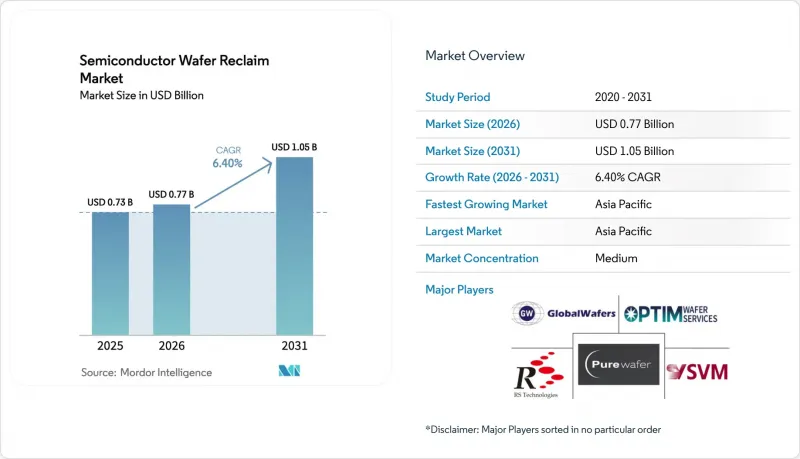
반도체 웨이퍼 재생 시장 규모는 2025년에 7억 3,000만 달러로 평가되었습니다. 2026년 7억 7,000만 달러에서 2031년까지 10억 5,000만 달러에 이를 것으로 예상되며, 예측 기간(2026-2031년) CAGR은 6.4%를 나타낼 전망입니다.

첨단 공정의 자본 집약도 증가와 순환 제조에 대한 규제 요건이 결합되어 반도체 제조업체들은 재생 웨이퍼로 전환하고 있습니다. 이러한 전환은 테스트 및 모니터용 웨이퍼의 총 소유 비용을 절감하고, 탄소 발자국을 줄이며, 새로운 웨이퍼의 가격이 계속 변동하는 상황에서 공급망 리스크를 완화할 수 있습니다. 또한, 인공지능(AI)을 활용한 검사로 처리 시간이 수일에서 수 시간으로 단축되어 재생 웨이퍼 벤더는 대량 생산을 하는 팹의 속도에 대응할 수 있게 되었습니다. 한편, 아시아태평양의 밀집된 300mm 팹 클러스터는 수요의 기반이 되고 있으며, 신흥 실리콘 카바이드(SiC) 및 질화갈륨(GaN) 파일럿 라인은 화합물 반도체 재생 시장에서 새로운 비즈니스 기회를 창출하고 있습니다. 95% 이상의 수율을 달성하기 위해 필요한 화학기계 연마(CMP) 및 계측 인프라가 자연스런 진입장벽으로 작용하고 있어 경쟁의 강도는 여전히 중간 정도에 머물러 있습니다.
세계의 반도체 웨이퍼 재생 시장 동향 및 인사이트
아시아태평양의 300mm 팹 생산 능력 확대
아시아태평양에서는 2027년까지 대부분의 신규 300mm 라인이 추가될 것으로 예상되며, 이는 각 팹의 월별 가동률의 15-20%를 차지하는 재생 테스트 웨이퍼의 기준 수요를 증가시킬 것입니다. 싱가포르와 대만의 신규 공장은 월 200만 장 이상의 웨이퍼를 추가 생산할 수 있으며, 이들 웨이퍼는 재생처리를 통해 각각 5회-7회 재사용이 가능해 반도체 웨이퍼 재생 시장의 물량 탄력성을 높이고 있습니다. 또한, 지역 내 집적도가 높기 때문에 물류 주기가 48시간 이내로 단축되어 재생 공급이 적시 생산 일정과 일치할 수 있도록 하고 있습니다. 따라서 각 벤더들은 메가팹 인근에 시설을 마련하고, 현금 흐름을 안정적으로 확보할 수 있는 다년 계약을 체결하고 있습니다. 생산 능력이 더욱 확대됨에 따라 재활용은 단순한 전술적 비용 절감 수단이 아닌 팹 계획의 구조적 요소로 자리 잡게 될 것입니다.
테스트 및 모니터용 웨이퍼에 대한 비용 최적화에 대한 압력
신규 테스트 웨이퍼는 현재 300mm당 120-150달러로 2024년 이후 18% 상승하여 로직, 메모리, 파워 팹의 매출 총이익률을 압박하고 있습니다. 재생 기판은 5-8회 사용 후 실제 비용을 25-35달러로 낮출 수 있어 즉각적인 비용 절감을 가져올 수 있습니다. 주요 파운드리 업체들은 재생 모니터 웨이퍼가 수율 저하 없이 측정 정확도를 충족하는 것을 입증했습니다. 디바이스 제조업체들도 머신러닝 모델을 도입하여 잔여 재생 주기를 예측하고, 표면 거칠기 한계치가 임계 임계치에 가까워진 경우에만 웨이퍼를 폐기하도록 하고 있습니다. 경제적인 이점은 성숙 노드에서 가장 두드러지지만, 현재 5nm 공정 시설에서도 챔버 시즈닝 등 소자 제조 이외의 공정에 웨이퍼를 재사용하고 있습니다.
2nm 노드에서의 엄격한 표면 결함 사양
2nm 노드 GaA(Gate All Around) 트랜지스터의 경우, 표면 결함 밀도가 1cm2당 0.1 개 미만의 결함 밀도를 요구하는데, 이는 재사용 공정에서 여러 번의 연마 사이클을 거친 후에도 보장하기 어려운 수준입니다. 원자층 수준의 세정 공정이 필요하기 때문에 웨이퍼 한 장당 15-20달러의 비용 증가가 발생하여 비용 절감 효과가 상쇄되기 때문에 첨단 노드 팹에서는 재생 웨이퍼의 사용이 중요하지 않은 공정에 국한되어 있습니다. 벤더들이 0.1nm 이하의 평탄도를 재현성 있게 입증하기 전까지는 최첨단 로직 라인에서 재생 웨이퍼의 도입이 제한될 것이며, 반도체 웨이퍼 재생 시장에서 가장 높은 가치를 지닌 부문의 성장 여지가 제한될 것입니다.
부문 분석
300mm 포맷은 2025년 매출의 52.84%를 차지했으며, 로직 및 메모리 팹용 반도체 웨이퍼 리사이클 시장 규모를 뒷받침하고 있습니다. 그러나 200mm 부문은 2026년부터 2031년까지 연평균 7.28% 성장할 것으로 예상되며, 다른 모든 직경보다 빠른 속도로 성장할 것으로 예측됩니다. 자동차 및 산업 분야의 기업들은 200mm 장비에 효율적으로 적합한 용도인 전력 관리 IC 및 마이크로 전자기계 시스템(MEMS)을 위해 성숙한 노드를 계속 선호하고 있습니다. 이 직경의 새로운 실리콘 카바이드 파일럿 라인은 대상 시장 기반을 더욱 확대할 것입니다. 리크라임 벤더는 기존 폴리셔에 엔드포인트 감지 센서를 장착하여 감가상각이 완료된 설비를 유지하면서 서브나노미터 수준의 제어를 실현함으로써 막대한 설비 투자 없이도 수익률을 향상시키고 있습니다. 전동화가 가속화됨에 따라, 300mm 라인이 절대적인 주도권을 유지하는 가운데, 200mm 리크라임의 생산량은 300mm 라인과의 매출 격차를 줄여나갈 것입니다.
150mm 리크라임에 대한 수요는 여전히 항공우주 분야와 내방사선 회로 분야에서 존재하며, 특수 다이의 비용 관리를 위해 작은 직경을 선호하는 위성 별자리가 이를 뒷받침하고 있습니다. 화합물 반도체 기판은 스케일업 전에 150mm로 도입되는 경우가 많으며, 이를 통해 공급업체는 향후 와이드 밴드갭 수요에 대한 진입 경로를 확보할 수 있습니다. 전반적으로, 이 직경 구성은 반도체 웨이퍼 재생 시장이 단순히 무어의 법칙의 진전뿐만 아니라 최종 용도의 경제성에 따라 어떻게 변화하는지를 잘 보여줍니다. 150mm에서 300mm 라인으로 사업을 다각화하는 업체는 특정 기술 사이클에 대한 의존도를 분산시키고, 각 직경이 새로운 중요성을 가질 때마다 단계적 성장을 포착할 수 있습니다.
지역별 분석
아시아태평양은 2025년 매출의 63.79%를 차지했으며, 2031년까지 연평균 6.92% 성장할 것으로 전망됩니다. 이는 전 세계 300mm 생산능력의 3분의 2 이상을 보유한 대만, 한국, 중국, 싱가포르가 주도하고 있습니다. 코로케이션 전략을 통해 웨이퍼 운송 시간을 2일 이내로 단축하고, 팹의 재공품 재고를 줄이는 한편, 리클레임이 운영의 필수 요소로 자리 잡았습니다. 중국의 '이중순환' 정책은 국내 리클레임 능력을 더욱 가속화하고, 지정학적 충격과 수출 규제에 대한 완충재로 현지 공급업체를 포지셔닝하고 있습니다.
북미는 2025년 매출의 약 18%를 차지했으며, CHIPS법 보조금으로 인해 애리조나주에서 텍사스주까지 신규 팹이 속속 건설되고 있습니다. 신공장은 자금 조달 지침에 포함된 순환 경제 설계 원칙을 반영하여 건설 초기부터 재생 베이가 통합되어 있습니다. 숙련된 인력 부족이 여전히 걸림돌로 작용하고 있지만, 커뮤니티 칼리지의 인증 프로그램이 그 격차를 메우기 시작했고, 중기적으로 지역 내 생산 능력의 확대가 증가하여 미국 반도체 웨이퍼 재생 시장 수요가 정착될 것임을 시사하고 있습니다.
유럽은 2025년 매출의 약 12%를 차지했으며, EU 칩스법에서 재생 실리콘 할당량을 의무화한 것이 벤더들의 수주 잔고를 뒷받침하고 있습니다. 이탈리아와 오스트리아의 공동 사업에서는 버진 실리콘과 재생 실리콘을 하나의 시설에서 통합하여 물류에 따른 배출량을 줄이고 규제 당국의 요구 사항을 충족하고 있습니다. 세계 다른 지역이 나머지 점유율을 차지하고 있으며, 이스라엘의 성숙한 마이크로일렉트로닉스 클러스터와 중동의 새로운 팹 건설 계획은 2028년 이후 추가 수요를 창출할 수 있습니다. 따라서 지역별 동향은 최종 시장의 소비가 아닌 팹 투자에 연동되어 있으며, 신규 웨이퍼 생산 시작에 자본이 유입되는 지역에 성장이 집중되고 있습니다.
기타 혜택 :
- 엑셀 형식 시장 예측(ME) 시트
- 3개월간 애널리스트 지원
자주 묻는 질문
목차
제1장 서론
제2장 조사 방법
제3장 주요 요약
제4장 시장 구도
제5장 시장 규모와 성장 예측
제6장 경쟁 구도
제7장 시장 기회와 향후 전망
KTH 26.05.29The semiconductor wafer reclaim market size was valued at USD 0.73 billion in 2025 and estimated to grow from USD 0.77 billion in 2026 to reach USD 1.05 billion by 2031, at a CAGR of 6.4% during the forecast period (2026-2031).
Heightened capital intensity at advanced nodes, paired with regulatory requirements for circular manufacturing, is steering integrated device manufacturers toward reclaimed substrates. The shift lowers total cost of ownership for test and monitor wafers, trims carbon footprints, and buffers supply-chain risk as virgin-wafer pricing stays volatile. Artificial-intelligence-driven inspection now compresses turnaround from days to hours, letting reclaim vendors match the cadence of high-volume fabs. Meanwhile, Asia-Pacific's dense 300 mm fab cluster anchors demand, while emerging silicon-carbide and gallium-nitride pilot lines open white-space opportunities in compound-semiconductor reclaim. Competitive intensity remains moderate because the chemical-mechanical polishing and metrology infrastructure required for yields above 95% creates natural entry barriers.
Global Semiconductor Wafer Reclaim Market Trends and Insights
Expanding 300 mm Fab Capacity In Asia-Pacific
Asia-Pacific is set to add the bulk of new 300 mm lines through 2027, lifting baseline demand for reclaimed test wafers that account for 15%-20% of every fab's monthly starts. New plants in Singapore and Taiwan add more than 2 million wafer starts per month, each of which can be reused five to seven times when reclaimed, driving volume elasticity for the semiconductor wafer reclaim market. Dense regional clustering also trims logistics to sub-48-hour cycles, aligning reclaim supply with just-in-time production schedules. Vendors are therefore co-locating facilities near megafabs, locking in multiyear contracts that stabilize cash flow. As additional capacity ramps, reclaim ceases to be a tactical cost lever and becomes a structural component of fab planning.
Cost-Optimization Pressure On Test And Monitor Wafers
Virgin test wafers now cost USD 120-USD 150 per 300 mm piece, up 18% since 2024, pinching gross margins for logic, memory, and power fabs. Reclaimed substrates drop the effective cost to USD 25-USD 35 after five to eight cycles, yielding immediate savings. Large foundries have validated that reclaimed monitor wafers meet metrology precision without yield loss. Device makers are also deploying machine-learning models to predict remaining reclaim cycles, ensuring wafers retire only when surface roughness limits approach critical thresholds. The economic case is strongest at mature nodes, but even 5 nm facilities now reclaim wafers for non-device steps such as chamber seasoning.
Stringent Surface-Defect Specs For 2 nm Node
Gate-all-around transistors at 2 nm demand surface-defect densities below 0.1 defects per cm2, a level reclaim processes struggle to guarantee after multiple polish cycles. The need for atomic-layer cleansing steps adds USD 15-USD 20 per wafer, eroding savings and confining reclaimed wafers to non-critical steps in advanced-node fabs. Until vendors demonstrate repeatable sub-0.1 nm flatness, leading-edge logic lines will cap reclaim penetration, limiting upside in the most valuable segment of the semiconductor wafer reclaim market.
Other drivers and restraints analyzed in the detailed report include:
- Sustainability Regulations Favoring Circular-Economy Practices
- AI-Enabled Yield-Imaging Tools Boosting Reclaim Yields
- Limited Skilled Labor For Advanced Polishing Lines
For complete list of drivers and restraints, kindly check the Table Of Contents.
Segment Analysis
The 300 mm format accounted for 52.84% of 2025 revenue, anchoring the semiconductor wafer reclaim market size for logic and memory fabs. Yet the 200 mm segment is forecast to rise at 7.28% during 2026-2031, outpacing all other diameters. Automotive and industrial players continue to favor mature nodes for power-management ICs and micro-electromechanical systems, applications that map efficiently onto 200 mm tooling. New silicon-carbide pilot lines at this diameter further widen the addressable base. Reclaim vendors retrofit legacy polishers with endpoint-detection sensors, delivering sub-nanometer control while preserving fully depreciated equipment, which lifts margins without heavy capital outlays. As electrification accelerates, 200 mm reclaim volume will narrow the revenue gap with 300 mm lines even though the latter retains absolute leadership.
Demand for 150 mm reclaim persists in niche aerospace and radiation-hardened circuits, aided by satellite constellations that prefer smaller diameters for cost control on specialized die. Compound-semiconductor substrates often debut at 150 mm before scaling, giving vendors an entry path into future wide-bandgap demand. Collectively, the diameter mix underscores how the semiconductor wafer reclaim market shifts with end-application economics, not just Moore's Law progression. Vendors diversified across 150 mm through 300 mm lines hedge exposure to any single technology cycle and capture step-wise growth as each diameter finds renewed relevance.
The Semiconductor Wafer Reclaim Market Report is Segmented by Wafer Diameter (Up To 150 Mm, 200 Mm, and More), Wafer Type (Test and Monitor Wafer Reclaim, Prime Wafer Reclaim, Epitaxial Wafer Reclaim, and More), Device Manufacturing Category (Memory Devices, Logic Devices, Analog and Power Devices, and More), and Geography. The Market Forecasts are Provided in Terms of Value (USD).
Geography Analysis
Asia-Pacific generated 63.79% of 2025 revenue and grows at 6.92% through 2031, powered by Taiwan, South Korea, China, and Singapore, which together host more than two-thirds of global 300 mm capacity. Co-location strategies shrink wafer-transit time to less than two days, lowering work-in-process inventory for fabs and cementing reclaim as an operational staple. China's dual-circulation policy further accelerates domestic reclaim capacity, treating local suppliers as a buffer against geopolitical shocks and export controls.
North America captured about 18% of 2025 turnover, but CHIPS Act subsidies are now spawning greenfield fabs from Arizona to Texas. New plants integrate reclaim bays at inception, reflecting circular-economy design principles embedded in funding guidelines. Skilled-labor shortages remain a drag, yet community-college certificate programs are beginning to close the gap, suggesting a medium-term uplift in regional capacity additions and cementing demand for the semiconductor wafer reclaim market in the United States.
Europe held roughly 12% of revenue in 2025, with the EU Chips Act mandating reclaimed-silicon quotas that underpin vendor order books. Co-located operations in Italy and Austria combine virgin and reclaim under one roof, trimming logistics emissions and satisfying regulators. Rest of World countries account for the balance, with Israel's mature microelectronics cluster and nascent Middle East fab proposals likely to seed incremental demand post-2028. Geography dynamics therefore track fab investments rather than end-market consumption, concentrating growth where capital flows into new wafer starts.
- RS Technologies Co., Ltd.
- Pure Wafer, Inc.
- GlobalWafers Co., Ltd.
- Optim Wafer Services Ltd.
- Silicon Valley Microelectronics, Inc.
- Phoenix Silicon International Corp.
- NanoSILICON, Inc.
- ReSilicon Group LLC
- Kay M Analytics Pte Ltd.
- Siltronic AG
- SUMCO Corporation
- Wafer World, Inc.
- Noel Technologies, Inc.
- PSEMI Corporation
- SiWave Technologies GmbH
- MicroTech Systems, Inc.
- WaferNET, Inc.
- Silicon Materials, Inc.
- REC Silicon ASA
- SilRec S.p.A.
Additional Benefits:
- The market estimate (ME) sheet in Excel format
- 3 months of analyst support
TABLE OF CONTENTS
1 INTRODUCTION
- 1.1 Study Assumptions and Market Definition
- 1.2 Scope of the Study
2 RESEARCH METHODOLOGY
3 EXECUTIVE SUMMARY
4 MARKET LANDSCAPE
- 4.1 Market Overview
- 4.2 Market Drivers
- 4.2.1 Expanding 300 mm Fab Capacity in Asia-Pacific
- 4.2.2 Cost-Optimisation Pressure on Test and Monitor Wafers
- 4.2.3 Sustainability Regulations Favouring Circular-Economy Practices
- 4.2.4 AI-Enabled Yield-Imaging Tools Boosting Reclaim Yields (Under-the-Radar)
- 4.2.5 Secondary-Market Demand from Low-Earth-Orbit Satellites (Under-the-Radar)
- 4.2.6 Foundry Shift to SiC/GaN Pilot Wafers Requiring Reclaim (Under-the-Radar)
- 4.3 Market Restraints
- 4.3.1 Stringent Surface-Defect Specs for 2 nm Node
- 4.3.2 Limited Skilled Labour for Advanced Polishing Lines
- 4.3.3 Uncertain Scrap-Silicon Pricing Volatility (Under-the-Radar)
- 4.3.4 Cyber-Security Risks in Fab-to-Reclaim Logistics (Under-the-Radar)
- 4.4 Impact of Macroeconomic Factors on the Market
- 4.5 Industry Value-Chain Analysis
- 4.6 Regulatory Landscape
- 4.7 Technological Outlook
- 4.8 Porter's Five Forces Analysis
- 4.8.1 Threat of New Entrants
- 4.8.2 Bargaining Power of Suppliers
- 4.8.3 Bargaining Power of Buyers
- 4.8.4 Threat of Substitutes
- 4.8.5 Intensity of Competitive Rivalry
5 MARKET SIZE AND GROWTH FORECASTS (VOLUME)
- 5.1 By Wafer Diameter
- 5.1.1 150 mm
- 5.1.2 200 mm
- 5.1.3 300 mm
- 5.2 By Wafer Type
- 5.2.1 Test and Monitor Wafer Reclaim
- 5.2.2 Prime Wafer Reclaim
- 5.2.3 Epitaxial Wafer Reclaim
- 5.2.4 SOI Wafer Reclaim
- 5.3 By Device Manufacturing Category
- 5.3.1 Memory Devices
- 5.3.2 Logic Devices
- 5.3.3 Analog and Power Devices
- 5.3.4 Specialty Devices (MEMS, Sensors, RF)
- 5.3.5 R&D Facilities
- 5.4 By Geography
- 5.4.1 North America
- 5.4.2 Europe
- 5.4.3 Asia-Pacific
- 5.4.4 Rest of the World
6 COMPETITIVE LANDSCAPE
- 6.1 Market Concentration
- 6.2 Strategic Moves
- 6.3 Market Share Analysis
- 6.4 Company Profiles (includes Global Level Overview, Market Level Overview, Core Segments, Financials as available, Strategic Information, Market Rank/Share, Products and Services, Recent Developments)
- 6.4.1 RS Technologies Co., Ltd.
- 6.4.2 Pure Wafer, Inc.
- 6.4.3 GlobalWafers Co., Ltd.
- 6.4.4 Optim Wafer Services Ltd.
- 6.4.5 Silicon Valley Microelectronics, Inc.
- 6.4.6 Phoenix Silicon International Corp.
- 6.4.7 NanoSILICON, Inc.
- 6.4.8 ReSilicon Group LLC
- 6.4.9 Kay M Analytics Pte Ltd.
- 6.4.10 Siltronic AG
- 6.4.11 SUMCO Corporation
- 6.4.12 Wafer World, Inc.
- 6.4.13 Noel Technologies, Inc.
- 6.4.14 PSEMI Corporation
- 6.4.15 SiWave Technologies GmbH
- 6.4.16 MicroTech Systems, Inc.
- 6.4.17 WaferNET, Inc.
- 6.4.18 Silicon Materials, Inc.
- 6.4.19 REC Silicon ASA
- 6.4.20 SilRec S.p.A.
7 MARKET OPPORTUNITIES AND FUTURE OUTLOOK
- 7.1 White-Space And Unmet-Need Assessment

