
|
시장보고서
상품코드
2071213
유리 기판 첨단 패키징 시장 : 비즈니스 기회, 성장요인, 업계 동향 분석 및 예측(2026-2035년)Glass Substrate Advanced Packaging Market Opportunity, Growth Drivers, Industry Trend Analysis, and Forecast 2026 - 2035 |
||||||
세계의 유리 기판 첨단 패키징 시장은 2025년에 20억 달러 규모가 되어, 2035년까지 연평균 복합 성장률(CAGR) 8.9%로 성장하여 47억 달러에 이를 것으로 추정되고 있습니다.

유리 기판 첨단 패키징 산업의 성장은 인공지능(AI) 및 고성능 컴퓨팅용 반도체 솔루션에 대한 수요 증가에 더해, 치플릿 기반 아키텍처와 패널 레벨 패키징 기술의 급속한 발전에 힘입어 주도되고 있습니다. 차세대 반도체 소자에서 고밀도 상호 연결에 대한 수요가 증가함에 따라 시장 확대가 더욱 가속화되고 있습니다. AI 가속기 및 첨단 데이터센터용 프로세서의 도입 확대는 기존 기판 기술에 큰 압박을 가하고 있으며, 유리 기반 솔루션으로의 전환을 촉진하고 있습니다. 유리 기판은 초미세 재배선층을 지원할 수 있어, 소형 칩 설계에서 전기적 성능 향상과 더 높은 배선 밀도를 실현할 수 있다는 점에서 주목받고 있습니다. 입출력 밀도의 향상, 뛰어난 신호 무결성, 그리고 확장 가능한 패키지 형식에 대한 수요가 증가함에 따라, 이 기술의 채택이 더욱 가속화되고 있습니다. 또한, 업계에서는 생태계의 지속적인 개발, 시범 규모 생산을 위한 노력, 그리고 유기 기판 소재의 한계를 극복하는 데 대한 관심이 높아지는 등의 혜택을 누리고 있습니다. 이러한 요인들이 복합적으로 작용하여, 첨단 패키징 분야에서 유리 기판의 장기적인 채택을 뒷받침하고 있습니다.
| 시장 범위 | |
|---|---|
| 시작 연도 | 2025년 |
| 예측 기간 | 2026-2035년 |
| 시작 연도 시장 규모 | 20억 달러 |
| 예측 금액 | 47억 달러 |
| CAGR | 8.9% |
2025년 기준으로, 붕규산 유리 부문은 44.9%의 시장 점유율을 차지했습니다. 이러한 우위는 열 안정성, 기계적 강도 및 비용 효율성이 탁월하게 조화를 이루고 있기 때문입니다. 또한, 이 소재가 기존의 반도체 제조 공정과 호환성이 있기 때문에 대량 생산 환경에서의 채택이 더욱 확대되고 있습니다. 이러한 특성 덕분에, 붕규산 유리는 첨단 패키징 용도를 위해 신뢰성이 높고 확장성이 뛰어난 기판 솔루션을 찾는 제조업체에게 최적의 선택지가 되고 있습니다.
하이브리드(TGV와 RDL의 조합) 부문은 2026년부터 2035년까지 연평균 성장률(CAGR) 12.6%로 성장할 것으로 전망됩니다. 이러한 성장은 설계 유연성 향상과 시스템 성능 강화를 가능하게 하는 통합형 수직 상호 연결 구조와 고해상도 재배선층(RDL)을 결합한 기술에 대한 수요 증가에 힘입어 이루어지고 있습니다. 하이브리드 패키징 기법은 복잡한 반도체 아키텍처에서 보다 효율적인 신호 배선, 집적 밀도 향상 및 확장성 향상을 실현합니다. 높은 상호 연결 성능과 최적화된 패키징 효율이 요구되는 첨단 칩 설계 분야에서 이 기술의 채택이 급속히 확대되고 있습니다.
2025년, 북미의 유리 기판 첨단 패키징 시장은 시장 점유율의 24.3%를 차지했습니다. 이 지역에서는 반도체 패키징 인프라, 연구시설 및 첨단 제조 역량에 대한 투자 확대에 힘입어 강력한 성장세를 보이고 있습니다. 국내 반도체 생산에 대한 집중도가 높아지고, AI 기반 칩 기술 분야의 혁신이 지역 내 수요를 더욱 강화하고 있습니다. 선진 패키징 생태계의 지속적인 개발을 통해 공급망의 회복탄력성이 향상되는 동시에, 북미 전역에서 차세대 기판 기술의 상용화가 가속화되고 있습니다.
자주 묻는 질문
목차
제1장 조사 방법과 범위
제2장 주요 요약
제3장 업계 인사이트
제4장 경쟁 구도
제5장 시장 추산 및 예측 : 소재 유형별, 2022-2035년
제6장 시장 추산 및 예측 : 패키징 아키텍처 유형별, 2022-2035년
제7장 시장 추산 및 예측 : 상호 접속 기술별, 2022-2035년
제8장 시장 추산 및 예측 : 최종 사용 산업별, 2022-2035년
제9장 시장 추산 및 예측 : 지역별, 2022-2035년
제10장 기업 개요
JHS 26.07.01The Global Glass Substrate Advanced Packaging Market was valued at USD 2 billion in 2025 and is estimated to grow at a CAGR of 8.9% to reach USD 4.7 billion by 2035.
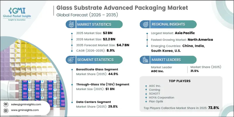
Growth in the glass substrate advanced packaging industry is driven by accelerating demand for artificial intelligence and high-performance computing semiconductor solutions, alongside rapid advancements in chiplet-based architectures and panel-level packaging technologies. Increasing requirements for high-density interconnects in next-generation semiconductor devices are further strengthening market expansion. Rising deployment of AI accelerators and advanced data center processors is placing significant pressure on traditional substrate technologies, driving the transition toward glass-based solutions. Glass substrates are gaining traction due to their ability to support ultra-fine redistribution layers, enabling improved electrical performance and higher interconnect density in compact chip designs. The growing need for enhanced input/output density, superior signal integrity, and scalable packaging formats is further reinforcing adoption. Additionally, the industry is benefiting from ongoing ecosystem development, pilot-scale production efforts, and increasing focus on overcoming the limitations of organic substrate materials. These factors collectively support the long-term adoption of glass substrates in advanced semiconductor packaging applications.
| Market Scope | |
|---|---|
| Start Year | 2025 |
| Forecast Year | 2026-2035 |
| Start Value | $2 Billion |
| Forecast Value | $4.7 Billion |
| CAGR | 8.9% |
The borosilicate glass segment held a 44.9% share in 2025. Its dominance is attributed to its strong balance of thermal stability, mechanical strength, and cost efficiency. The material's compatibility with established semiconductor manufacturing processes has further strengthened its adoption in high-volume production environments. These properties make borosilicate glass a preferred option for manufacturers seeking reliable and scalable substrate solutions for advanced electronic packaging applications.
The hybrid (TGV combined with RDL) segment is projected to grow at a CAGR of 12.6% during 2026-2035. This growth is driven by increasing demand for integrated vertical interconnect structures combined with high-resolution redistribution layers, enabling improved design flexibility and enhanced system performance. Hybrid packaging approaches support more efficient signal routing, improved integration density, and greater scalability for complex semiconductor architectures. Their adoption is expanding rapidly in advanced chip designs that require high interconnect performance and optimized packaging efficiency.
North America Glass Substrate Advanced Packaging Market accounted for 24.3% share in 2025. The region is witnessing strong growth supported by rising investments in semiconductor packaging infrastructure, research facilities, and advanced manufacturing capabilities. Expanding focus on domestic semiconductor production and innovation in AI-driven chip technologies is further strengthening regional demand. Continued development of advanced packaging ecosystems is enhancing supply chain resilience while accelerating the commercialization of next-generation substrate technologies across North America.
Key companies operating in the global glass substrate advanced packaging market include Corning, Intel Corporation, SCHOTT, AGC Inc., HOYA Corporation, AT&S (Austria Technologie & Systemtechnik), Nippon Sheet Glass Co., Ltd., Avanstrate Inc., NEG (Nippon Electric Glass Co., Ltd.), Absolics, Plan Optik, Ohara Inc., Mosaic Microsystems, TOPPAN, and Shyawei Optronics (Taiwan). Companies participating in the glass substrate advanced packaging industry are focusing on strategic initiatives aimed at strengthening technological capabilities and expanding market presence. A major emphasis is placed on research and development to improve substrate performance, enhance thermal and electrical properties, and enable finer interconnect scaling for next-generation semiconductor devices. Market participants are also investing in pilot production lines and scaling up manufacturing capacity to support the commercialization of advanced packaging solutions. Strategic collaborations with semiconductor manufacturers, foundries, and technology developers are helping accelerate innovation and ecosystem development. In addition, companies are working on improving process integration, cost efficiency, and material optimization to enhance competitiveness.
Table of Contents
Chapter 1 Methodology and Scope
- 1.1 Market scope and definition
- 1.2 Research design
- 1.2.1 Research approach
- 1.2.2 Data collection methods
- 1.3 Data mining sources
- 1.3.1 Global
- 1.3.2 Regional/Country
- 1.4 Base estimates and calculations
- 1.4.1 Base year calculation
- 1.4.2 Key trends for market estimation
- 1.5 Primary research and validation
- 1.5.1 Primary sources
- 1.6 Forecast model
- 1.7 Research assumptions and limitations
Chapter 2 Executive Summary
- 2.1 Industry 360° synopsis, 2022 - 2035
- 2.2 Key market trends
- 2.2.1 Material type trends
- 2.2.2 Packaging architecture type trends
- 2.2.3 Interconnect technology trends
- 2.2.4 End-user industry trends
- 2.2.5 Regional trends
- 2.3 TAM Analysis, 2026-2035
- 2.4 CXO perspectives: Strategic imperatives
Chapter 3 Industry Insights
- 3.1 Industry ecosystem analysis
- 3.1.1 Supplier Landscape
- 3.1.2 Profit Margin
- 3.1.3 Cost structure
- 3.1.4 Value addition at each stage
- 3.1.5 Factor affecting the value chain
- 3.1.6 Disruptions
- 3.2 Industry impact forces
- 3.2.1 Growth drivers
- 3.2.1.1 Rising AI, HPC demand requiring higher interconnect density
- 3.2.1.2 Glass substrates enable ultra-fine line redistribution layers
- 3.2.1.3 Superior thermal stability vs organic substrates
- 3.2.1.4 Increasing chiplet-based heterogeneous integration adoption
- 3.2.1.5 Panel-level packaging improves cost efficiency at scale
- 3.2.2 Industry pitfalls and challenges
- 3.2.2.1 Limited ecosystem readiness vs organic substrates
- 3.2.2.2 Fragility concerns during handling and manufacturing
- 3.2.3 Market opportunities
- 3.2.3.1 Adoption in next-gen AI accelerators and data center chips
- 3.2.3.2 Expansion into automotive high-performance computing systems
- 3.2.1 Growth drivers
- 3.3 Growth potential analysis
- 3.4 Regulatory landscape
- 3.4.1 North America
- 3.4.2 Europe
- 3.4.3 Asia Pacific
- 3.4.4 Latin America
- 3.4.5 Middle East & Africa
- 3.5 Porter's analysis
- 3.6 PESTEL analysis
- 3.7 Technology and Innovation landscape
- 3.7.1 Current technological trends
- 3.7.2 Emerging technologies
- 3.8 Price trends
- 3.8.1 By region
- 3.8.2 By product
- 3.9 Pricing Strategies
- 3.10 Emerging Business Models
- 3.11 Compliance Requirements
- 3.12 Patent and IP analysis
Chapter 4 Competitive Landscape, 2025
- 4.1 Introduction
- 4.2 Company market share analysis
- 4.2.1 By region
- 4.2.1.1 North America
- 4.2.1.2 Europe
- 4.2.1.3 Asia Pacific
- 4.2.1.4 Latin America
- 4.2.1.5 Middle East & Africa
- 4.2.2 Market concentration analysis
- 4.2.1 By region
- 4.3 Competitive benchmarking of key players
- 4.3.1 Financial performance comparison
- 4.3.1.1 Revenue
- 4.3.1.2 Profit margin
- 4.3.1.3 R&D
- 4.3.2 Product portfolio comparison
- 4.3.2.1 Product range breadth
- 4.3.2.2 Technology
- 4.3.2.3 Innovation
- 4.3.3 Geographic presence comparison
- 4.3.3.1 Global footprint analysis
- 4.3.3.2 Service network coverage
- 4.3.3.3 Market penetration by region
- 4.3.4 Competitive positioning matrix
- 4.3.4.1 Leaders
- 4.3.4.2 Challengers
- 4.3.4.3 Followers
- 4.3.4.4 Niche players
- 4.3.5 Strategic outlook matrix
- 4.3.1 Financial performance comparison
- 4.4 Key developments
- 4.4.1 Mergers and acquisitions
- 4.4.2 Partnerships and collaborations
- 4.4.3 Technological advancements
- 4.4.4 Expansion and investment strategies
- 4.4.5 Digital transformation initiatives
- 4.5 Emerging/ startup competitors landscape
Chapter 5 Market Estimates and Forecast, By Material Type, 2022 - 2035 (USD Million)
- 5.1 Key trends
- 5.2 Borosilicate glass
- 5.3 Aluminosilicate glass
- 5.4 Fused silica / quartz
- 5.5 Specialty engineered glasses
Chapter 6 Market Estimates and Forecast, By Packaging Architecture Type, 2022 - 2035 (USD Million)
- 6.1 Key trends
- 6.2 2.5D interposer packages
- 6.3 3D-IC / chiplet packages
- 6.4 Fan-out wafer-level packages (FOWLP)
- 6.5 Co-packaged optics / photonics packages
Chapter 7 Market Estimates and Forecast, By Interconnect Technology, 2022 - 2035 (USD Million)
- 7.1 Key trends
- 7.2 Through-glass via (TGV)
- 7.3 Redistribution layer (RDL)
- 7.4 Hybrid (TGV + RDL)
Chapter 8 Market Estimates and Forecast, By End-User Industry, 2022 - 2035 (USD Million)
- 8.1 Key trends
- 8.2 Data centers
- 8.3 Telecommunications
- 8.4 Consumer electronics
- 8.5 Automotive
- 8.6 Aerospace & defense
Chapter 9 Market Estimates and Forecast, By Region, 2022 - 2035 (USD Million)
- 9.1 Key trends
- 9.2 North America
- 9.2.1 U.S.
- 9.2.2 Canada
- 9.3 Europe
- 9.3.1 Germany
- 9.3.2 UK
- 9.3.3 France
- 9.3.4 Spain
- 9.3.5 Italy
- 9.3.6 Netherlands
- 9.4 Asia Pacific
- 9.4.1 China
- 9.4.2 India
- 9.4.3 Japan
- 9.4.4 Australia
- 9.4.5 South Korea
- 9.5 Latin America
- 9.5.1 Brazil
- 9.5.2 Mexico
- 9.5.3 Argentina
- 9.6 Middle East and Africa
- 9.6.1 South Africa
- 9.6.2 Saudi Arabia
- 9.6.3 UAE
Chapter 10 Company Profiles
- 10.1 Global Key Players
- 10.1.1 AGC Inc.
- 10.1.2 Corning
- 10.1.3 SCHOTT
- 10.1.4 HOYA Corporation
- 10.1.5 Intel Corporation
- 10.2 Regional key players
- 10.2.1 North America
- 10.2.1.1 Mosaic Microsystems
- 10.2.2 Asia Pacific
- 10.2.2.1 Absolics
- 10.2.2.2 NEG (Nippon Electric Glass Co., Ltd.)
- 10.2.2.3 Nippon Sheet Glass Co., Ltd.
- 10.2.2.4 Ohara Inc.
- 10.2.2.5 Shyawei Optronics (Taiwan)
- 10.2.2.6 TOPPAN
- 10.2.3 Europe
- 10.2.3.1 AT&S (Austria Technologie & Systemtechnik)
- 10.2.3.2 Plan Optik
- 10.2.1 North America
- 10.3 Niche Players/Disruptors
- 10.3.1 Avanstrate Inc.
