
|
시장보고서
상품코드
2065435
GPU 아키텍처 및 컴퓨트 IP 라이선싱 : 시장 점유율 분석, 업계 동향 및 통계, 성장 예측(2026-2031년)GPU Architecture And Compute IP Licensing - Market Share Analysis, Industry Trends & Statistics, Growth Forecasts (2026 - 2031) |
||||||
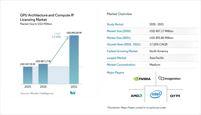
GPU 아키텍처 및 컴퓨트 IP 라이선싱 시장 규모는 2025년 3억 4,792만 달러로 평가되었습니다. 2026년에는 4억 717만 달러로 확대되어 2031년까지 8억 9,385만 달러에 이를 것으로 예상되며 2026년부터 2031년에 걸쳐 CAGR 17.03%로 성장할 전망입니다.

본 보고서는 IP의 유형(GPU 코어 IP, AI/텐서 연산 IP, 연산 ISA/아키텍처 IP, 온칩 연산 상호 연결 IP), 라이선싱 모델(영구 라이선스 + 로열티, 구독/접근 기반 라이선싱 등), 최종 사용자(팹리스 반도체 기업, 집적 소자 제조업체 등), 지역별로 분류되어 있습니다. 시장 전망은 금액(달러) 기준으로 제시되어 있습니다.
세계의 GPU 아키텍처 및 컴퓨트 IP 라이선싱 시장 동향 및 인사이트
데이터센터 내 AI 워크로드의 폭발적인 증가
하이퍼스케일 클라우드 제공업체들은 텐서 코어 IP 라이선싱을 취득하여, 추론당 에너지 비용을 절감하고, 디스크리트 GPU의 마진 압박을 피할 수 있는 용도 특화형 가속기를 구축하고 있습니다. 2025년 3월에 도입된 AWS의 Trainium2 인스턴스는 H100 클러스터에 비해 와트당 성능이 30% 향상되었으며, 이를 통해 사업자의 연간 GPU 구매 비용을 12억 달러 절감하고 있습니다. 구글의 TPU v6e는 브로드컴과 공동 개발한 것으로, 동급 GPU 팜에 비해 에너지 비용을 3분의 1로 줄였습니다. 200억 달러 규모의 엔비디아와 Groq 간의 계약은 추론에 특화된 스타트업조차 로드맵의 유연성을 유지하기 위해 IP 접근을 요구하게 되었음을 입증했습니다. 이러한 라이선싱 추세는 수익 확대를 가속화할 것입니다. 왜냐하면 ‘영구 라이선스 + 로열티’ 또는 구독 모델을 통해 하이퍼스케일러는 공급 계약을 재협상할 필요 없이 18개월마다 시스템을 업데이트할 수 있기 때문입니다. 그 결과 발생하는 수요 증가는 전체 연평균 성장률(CAGR) 전망에 5.2%의 긍정적 기여를 가져올 것입니다.
엣지 AI 기기의 보급
스마트폰, 소비자용 IoT 노드, 스마트 가전에는 개인정보 보호 요건을 충족하고 100밀리초 미만의 지연 시간 요건을 충족할 수 있는 기기 내 생성 모델이 요구되고 있습니다. 퀄컴의 ‘Snapdragon 8 Elite’는 실시간 영상 세분화을 위해 45 TOPS의 처리 능력을 갖춘 AI 텐서 슬라이스를 통합하고 있습니다. MediaTek의 Dimensity 9400은 Arm Mali-G925GPU IP와 16코어 NPU를 결합하여 70억 파라미터 규모의 모델을 로컬에서 실행합니다. Arm은 Mali 및 Immortalis를 탑재한 SoC의 출하량이 18억 개에 달함에 따라, 2025 회계연도의 로열티 수입이 34% 증가했다고 보고했습니다. 이매지네이션의 IMG CXT가 레벨 3 ADAS 소켓을 확보함에 따라, 자동차 분야 수요가 더욱 큰 호재로 작용하고 있습니다. 폭넓은 설계 도입 실적이 예측 연평균 성장률(CAGR) 3.8% 상승을 뒷받침하고 있습니다.
선진 노드에서 발생하는 고액의 초기 NRE 비용
3nm 및 2nm 공정의 마스크 세트 비용은 현재 3,000만 달러를 초과하며, 첫 실리콘 제작 비용은 8,000만 달러에 달하기도 하여, 많은 중견 팹리스 기업들이 최첨단 설계 시장에서 배제되고 있습니다. CoWoS 패키징 비용은 다이당 1,500달러로, 2023년의 900달러에서 상승했습니다. 삼성의 3nm 게이트 올 어라운드(GAA) 노드는 15% 더 저렴하지만, 초기 테이프아웃 과정에서 6개월의 지연이 발생했습니다. 이에 대한 대책으로, 소규모 라이선스 취득 기업들은 전력 효율을 희생하면서 성숙한 7nm 노드로의 전환이나 치플릿 도입을 추진하고 있습니다. 이러한 투자 장벽으로 인해 예측 연평균 성장률(CAGR)이 2.8% 하락했습니다.
부문별 분석
GPU 코어 IP는 2025년에 매출 점유율의 44%를 차지했으나, 이러한 입지는 연간 20억 대 이상의 기기에 탑재된 Arm Mali 및 Imagination PowerVR의 프랜차이즈를 통해 구축된 것입니다. 각 하이퍼스케일러 기업들이 래스터화보다 INT8 및 스파스니스 엔진을 우선시하고, 예산을 특수한 행렬 처리 블록으로 전환함에 따라 AI 및 텐서 연산 IP 시장은 연평균 성장률(CAGR) 21.90%로 확대되고 있습니다. Nvidia와 Groq의 제휴는 라이선스 보유사들이 수출 규제를 준수하는 추론용 칩을 위해 Blackwell 세대의 텐서 코어와 NVLink 패브릭을 점점 더 중시하고 있음을 보여줍니다. 주로 RISC-V 벡터 확장으로 구성된 연산 ISA IP는 로열티가 없는 명령어 세트를 추구하는 유럽 및 인도의 자체 개발 프로그램의 뒷받침을 받아 18%의 시장 점유율을 차지했습니다. 칩렛의 도입에 따라 100나노초 미만의 지연 시간을 실현하는 메쉬가 필요해짐에 따라, 온칩 상호 연결 IP 시장 점유율은 14%에 달했습니다.
각 하이퍼스케일러 기업들은 와트당 연산 성능을 향상시키는 스파스 텐서 가속기를 선호하고 있으며, 구글의 TPU v6e가 그 대표적인 예입니다. 이 제품은 맞춤형 스파스 로직을 통합함으로써 밀행렬 처리의 처리량을 2.4배로 높였습니다. Meta의 MTIA v2는 독자적인 추론 유닛을 설계하는 한편, 메모리 컨트롤러와 상호 연결 블록에 대해서만 라이선스를 부여했습니다. SiFive의 Intelligence X390 NPU는 RISC-V 벡터와 128레인 행렬 엔진을 융합하여, 라이선스 사용자에게 5와트 소비로 50 TOPS를 달성할 수 있는 로열티 프리 솔루션을 제공합니다. 그 결과, AI 중심 IP는 2031년까지 기존의 GPU 셰이더 코어를 추월할 것으로 전망됩니다.
지역별 분석
2025년, 아시아태평양은 GPU 아키텍처 및 연산 IP 라이선싱 시장 점유율의 46%를 차지했으며, 그 중심에는 전 세계 라이선스된 GPU 설계의 70% 이상을 생산하는 대만의 TSMC가 있었습니다. 중국은 수출 규제라는 역풍에도 불구하고, 국내 GPU 개발에 450억 위안(63억 달러)을 배정했습니다. 인도의 ‘Design Linked Incentive’ 제도는 IP 사용료의 최대 50%를 환급해 주는 제도로, 이를 통해 Imagination, SiFive, Cadence가 현지 파트너십에 참여하고 있습니다. 일본은 Rapidus 컨소시엄을 통해 RISC-V GPU IP에 2,000억 엔(13억 달러)을 투자했습니다. Biren과 Moore Threads는 Arm 및 Synopsys의 IP에 대한 접근 권한을 상실했으나, 두 회사 모두 알리바바의 로열티가 없는 Xuantie C930 코어로 사업 방향을 전환했습니다.
북미 시장은 CHIPS법의 인센티브와 하이퍼스케일러들의 수직 통합에 힘입어 2031년까지 연평균 성장률(CAGR) 19.20%로 확대될 것으로 전망됩니다. AWS, Google, Meta는 2025년에 맞춤형 실리콘 IP에 80억 달러 이상을 투자할 예정이며, TSMC의 애리조나 공장에서는 2026년 1분기부터 Trainium 2 및 TPU v6e의 양산을 시작할 예정입니다. 2024년 10월 미국의 수출 규제 개정으로 인해, 공급업체들은 지역별 규정 준수 요건에 맞추어 ASIC을 조정해야 했기 때문에 의도치 않게 국내에서의 라이선스 취득이 가속화되었습니다.
유럽은 2025년에 12%의 시장 점유율을 기록했으며, 자동차용 ADAS와 소버린 컴퓨팅이 수요를 주도했습니다. 유럽 프로세서 이니셔티브는 Rhea2 엑사스케일 프로세서를 위해 SiFive의 RISC-V 벡터 프로세서 라이선스를 취득했습니다. 독일은 자동차 공급망 내 GPU IP에 대한 지원금으로 5억 유로(5억 6,500만 달러)를 예산에 편성했습니다. 남미, 중동 및 아프리카를 포함한 ‘세계 기타 지역’은 지적재산권 보호 집행이 미흡하고, 파브(반도체 제조 공장)의 생산 능력도 제한적이어서, 전체 시장 점유율이 6%에 그쳤습니다.
기타 혜택 :
- 엑셀 형식 시장 예측(ME) 시트
- 3개월간의 애널리스트 지원
자주 묻는 질문
목차
제1장 서론
제2장 조사 방법
제3장 주요 요약
제4장 시장 구도
제5장 시장 규모 및 성장 예측
제6장 경쟁 구도
제7장 시장 기회 및 향후 전망
KTH 26.06.29According to Mordor Intelligence, the graphics processing unit (GPU) architecture and Compute Intellectual Property (IP) Licensing Market size is expected to increase from USD 347.92 million in 2025 to USD 407.17 million in 2026 and reach USD 893.85 million by 2031, growing at a CAGR of 17.03% over 2026-2031.
This report is Segmented by IP Type (GPU Core IP, AI/Tensor Compute IP, Compute ISA/Architecture IP, On-Chip Compute Interconnect IP), Licensing Model (Perpetual License + Royalty, Subscription/Access-Based Licensing, and More), End User (Fabless Semiconductor Companies, Integrated Device Manufacturers, and More), and Geography. The Market Forecasts are Provided in Terms of Value (USD).
Global GPU Architecture And Compute IP Licensing Market Trends and Insights
Explosive AI Workload Growth In Data Centers
Hyperscale cloud providers are licensing tensor-core IP to build application-specific accelerators that trim energy cost per inference and avoid the margin stack of discrete GPUs. AWS Trainium2 instances, rolled out in March 2025, deliver 30% better performance per watt than H100 clusters, cutting the operator's annual GPU purchase bill by USD 1.2 billion.Google's TPU v6e, co-developed with Broadcom, achieves one-third the energy cost of comparable GPU farms. The USD 20 billion Nvidia-Groq agreement proved that even inference-focused start-ups now seek IP access to preserve roadmap flexibility. This licensing preference accelerates revenue because perpetual-plus-royalty or subscription models let hyperscalers iterate every 18 months without renegotiating supply contracts. Resulting demand growth drives a positive 5.2% contribution to the overall CAGR forecast.
Proliferation Of Edge AI Devices
Smartphones, consumer IoT nodes, and smart-home appliances require on-device generative models that satisfy privacy mandates and sub-100 millisecond latency budgets. Qualcomm's Snapdragon 8 Elite integrates AI tensor slices capable of 45 TOPS for real-time video segmentation. MediaTek's Dimensity 9400 combines Arm Mali-G925 GPU IP with a 16-core NPU to locally run 7-billion-parameter models.Arm reported a 34% royalty jump in fiscal 2025 on shipments of 1.8 billion Mali- and Immortalis-equipped SoCs. Automotive demand adds further momentum as Imagination's IMG CXT wins Level 3 ADAS sockets. The breadth of design wins underpins a 3.8% uplift to forecast CAGR.
High Up-Front NRE Costs For Advanced Nodes
Mask sets for 3 nm and 2 nm processes now exceed USD 30 million, and first-silicon outlays can reach USD 80 million, pricing many mid-tier fabless firms out of leading-edge designs. CoWoS packaging adds USD 1,500 per die, up from USD 900 in 2023. Samsung's 3 nm gate-all-around node is 15% cheaper but yielded six-month delays in early tape-outs. As a workaround, smaller licensees migrate to mature 7 nm nodes or adopt chiplets, sacrificing power efficiency. The spending barrier removes 2.8% from the projected CAGR.
Other drivers and restraints analyzed in the detailed report include:
- Rising GPU Adoption In Automotive ADAS
- Mainstreaming Of Ray Tracing In Consumer Graphics
- Export Controls On High-Performance Compute IP
For complete list of drivers and restraints, kindly check the Table Of Contents.
Segment Analysis
GPU core IP held 44% revenue share in 2025, a position built on Arm Mali and Imagination PowerVR franchises that ship in more than 2 billion devices annually. AI and tensor compute IP is expanding at a 21.90% CAGR as hyperscalers prioritize INT8 and sparsity engines over rasterization, redirecting spend toward specialized matrix blocks. The Nvidia-Groq arrangement illustrates how licensees increasingly value Blackwell-generation tensor cores and NVLink fabrics for export-compliant inference chips. Compute ISA IP, primarily RISC-V vector extensions, captured 18% share, buoyed by sovereign programs in Europe and India that seek royalty-free instruction sets. On-chip interconnect IP reached 14% share as chiplet adoption demands sub-100-nanosecond latency meshes.
Hyperscalers also favor sparse-tensor accelerators that boost operations per watt, as seen in Google's TPU v6e, which integrates custom sparsity logic yielding 2.4X dense-matrix throughput. Meta's MTIA v2 licensed only memory-controller and interconnect blocks while designing proprietary inference units. SiFive's Intelligence X390 NPU blends RISC-V vectors with a 128-lane matrix engine, offering licensees a royalty-free path to 50 TOPS at 5 watts. As a result, AI-centric IP is positioned to overtake classic GPU shader cores before 2031.
Geography Analysis
Asia-Pacific held 46% of the GPU architecture and compute IP licensing market share in 2025, anchored by Taiwan's TSMC, which fabricates more than 70% of licensed GPU designs worldwide. China earmarked CNY 45 billion (USD 6.3 billion) for domestic GPU development despite export-control headwinds. India's Design Linked Incentive reimburses up to 50% of IP fees, drawing Imagination, SiFive, and Cadence into local partnerships. Japan committed JPY 200 billion (USD 1.3 billion) to RISC-V GPU IP via the Rapidus consortium. Although Biren and Moore Threads lost access to Arm and Synopsys IP, both pivoted to Alibaba's royalty-free Xuantie C930 cores.
North America is projected to expand at a 19.20% CAGR through 2031, fueled by CHIPS Act incentives and hyperscaler vertical integration. AWS, Google, and Meta invested more than USD 8 billion in custom-silicon IP during 2025, and TSMC's Arizona fab will produce Trainium2 and TPU v6e volumes from Q1 2026. The October 2024 U.S. export-control update inadvertently accelerated domestic licensing, as providers now must tailor ASICs for regional compliance.
Europe captured 12% share in 2025, with automotive ADAS and sovereign compute driving demand. The European Processor Initiative licensed SiFive RISC-V vectors for its Rhea2 exascale processor. Germany budgeted EUR 500 million (USD 565 million) to subsidize GPU IP in the auto supply chain. Rest-of-World regions, including South America, Middle East, and Africa, together represented 6% share, hindered by weaker IP-protection enforcement and limited fab capacity.
- Arm Ltd.
- Imagination Technologies Ltd.
- Nvidia Corporation
- Advanced Micro Devices, Inc.
- Intel Corporation
- SiFive, Inc.
- Tenstorrent, Inc.
- VeriSilicon Microelectronics Co., Ltd.
- Synopsys, Inc.
- Cadence Design Systems, Inc.
- Alibaba Group Holding Ltd. (T-Head)
- Qualcomm Technologies, Inc.
- Samsung Electronics Co., Ltd.
- Apple Inc.
- Broadcom Inc.
- Meta Platforms, Inc. (AI Research ASICs)
- Google LLC (TPU IP Licensing)
- Graphcore Ltd.
- Rivos, Inc.
- Esperanto Technologies, Inc.
Additional Benefits:
- The market estimate (ME) sheet in Excel format
- 3 months of analyst support
TABLE OF CONTENTS
1 INTRODUCTION
- 1.1 Study Assumptions and Market Definition
- 1.2 Scope of the Study
2 RESEARCH METHODOLOGY
3 EXECUTIVE SUMMARY
4 MARKET LANDSCAPE
- 4.1 Market Overview
- 4.2 Market Drivers
- 4.2.1 Explosive AI Workload Growth in Data Centers
- 4.2.2 Proliferation of Edge AI Devices
- 4.2.3 Rising GPU Adoption in Automotive ADAS
- 4.2.4 Mainstreaming of Ray Tracing in Consumer Graphics
- 4.2.5 Sovereign Semiconductor Strategies Driving In-House IP
- 4.2.6 Open-Source ISA Momentum (e.g., RISC-V) Catalyzing Custom GPUs
- 4.3 Market Restraints
- 4.3.1 High Up-Front NRE Costs for Advanced Nodes
- 4.3.2 Export Controls on High-Performance Compute IP
- 4.3.3 Fragmentation of Software Toolchains
- 4.3.4 Escalating Patent Litigation Risk
- 4.4 Industry Value / Supply-Chain Analysis
- 4.5 Regulatory Landscape
- 4.6 Technological Outlook
- 4.7 Impact of Macroeconomic Factors on the Market
- 4.8 Porter's Five Forces Analysis
- 4.8.1 Bargaining Power of Buyers
- 4.8.2 Bargaining Power of Suppliers
- 4.8.3 Threat of New Entrants
- 4.8.4 Threat of Substitutes
- 4.8.5 Competitive Rivalry
5 MARKET SIZE AND GROWTH FORECASTS (VALUE)
- 5.1 By IP Type
- 5.1.1 GPU Core IP
- 5.1.2 AI / Tensor Compute IP
- 5.1.3 Compute ISA / Architecture IP
- 5.1.4 On-Chip Compute Interconnect IP
- 5.2 By Licensing Model
- 5.2.1 Perpetual License + Royalty
- 5.2.2 Subscription / Access-Based Licensing
- 5.2.3 Royalty-Only Models
- 5.3 By End User
- 5.3.1 Fabless Semiconductor Companies
- 5.3.2 Integrated Device Manufacturers (IDMs)
- 5.3.3 Hyperscalers
- 5.4 By Geography
- 5.4.1 North America
- 5.4.1.1 United States
- 5.4.1.2 Canada
- 5.4.1.3 Mexico
- 5.4.2 Europe
- 5.4.2.1 United Kingdom
- 5.4.2.2 Germany
- 5.4.2.3 France
- 5.4.2.4 Italy
- 5.4.2.5 Rest of Europe
- 5.4.3 Asia-Pacific
- 5.4.3.1 China
- 5.4.3.2 Japan
- 5.4.3.3 India
- 5.4.3.4 South Korea
- 5.4.3.5 Rest of Asia-Pacific
- 5.4.4 Rest of the World
- 5.4.1 North America
6 COMPETITIVE LANDSCAPE
- 6.1 Market Concentration
- 6.2 Strategic Moves
- 6.3 Market Share Analysis
- 6.4 Company Profiles (includes Global Level Overview, Market Level Overview, Core Segments, Financials as available, Strategic Information, Market Rank/Share, Products and Services, Recent Developments)
- 6.4.1 Arm Ltd.
- 6.4.2 Imagination Technologies Ltd.
- 6.4.3 Nvidia Corporation
- 6.4.4 Advanced Micro Devices, Inc.
- 6.4.5 Intel Corporation
- 6.4.6 SiFive, Inc.
- 6.4.7 Tenstorrent, Inc.
- 6.4.8 VeriSilicon Microelectronics Co., Ltd.
- 6.4.9 Synopsys, Inc.
- 6.4.10 Cadence Design Systems, Inc.
- 6.4.11 Alibaba Group Holding Ltd. (T-Head)
- 6.4.12 Qualcomm Technologies, Inc.
- 6.4.13 Samsung Electronics Co., Ltd.
- 6.4.14 Apple Inc.
- 6.4.15 Broadcom Inc.
- 6.4.16 Meta Platforms, Inc. (AI Research ASICs)
- 6.4.17 Google LLC (TPU IP Licensing)
- 6.4.18 Graphcore Ltd.
- 6.4.19 Rivos, Inc.
- 6.4.20 Esperanto Technologies, Inc.
7 MARKET OPPORTUNITIES AND FUTURE OUTLOOK
- 7.1 White-Space and Unmet-Need Assessment
