
|
시장보고서
상품코드
2065506
Ajinomoto 빌드업 필름(ABF) 기판 시장 : 시장 점유율 분석, 업계 동향 및 통계, 성장 예측(2026-2031년)Ajinomoto Build-Up Film (ABF) Substrate - Market Share Analysis, Industry Trends & Statistics, Growth Forecasts (2026 - 2031) |
||||||
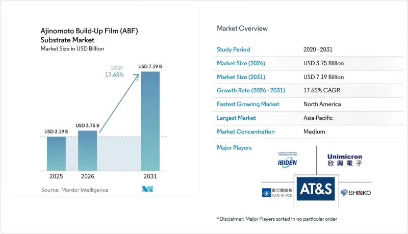
Ajinomoto 빌드업 필름(ABF) 기판 시장 규모는 2025년 31억 9,000만 달러로 평가되었고, 2026년 37억 5,000만 달러로 추정되고, 2031년까지 71억 9,000만 달러로 확대할 것으로 예측되며, 2026-2031년 연평균 복합 성장률(CAGR)은 17.65%를 나타낼 전망입니다.

본 보고서는 패키지 유형별(플립칩 BGA, 플립칩 CSP), 용도별(AI GPU, CPU, AI 가속기, 네트워크 IC), 최종 사용자 산업별(데이터센터, 소비자용 전자기기, 자동차, 통신) 및 지역별(북미, 유럽, 아시아태평양, 기타 지역)로 분류되어 있습니다. 시장 전망은 금액(달러) 기준으로 제시되어 있습니다.
세계의 Ajinomoto 빌드업 필름(ABF) 기판 시장 동향 및 인사이트
AI GPU 패키지에서 ABF 기판의 채택 확대
NVIDIA H200이나 AMD MI300과 같은 차세대 AI GPU에서는 뒤틀림을 줄이기 위해 12-20층의 빌드업 층, 15µm 미만의 라인·스페이스, 2 ppm/°C 이내의 열팽창계수(CTE) 일관성이 요구되고 있으며, 이에 따라 Ajinomoto 빌드업 필름(ABF) 기판 시장 수요는 사상 최고 수준에 달하고 있습니다. 이비덴은 이러한 GPU를 명확한 목표로 삼아, 2027년도에 순차적으로 양산을 시작할 예정인 일본 내 2곳의 파브에 5,000억 엔(33억 달러)을 투자하기로 결정했습니다. 멀티치플렛 레이아웃에서는 패키지당 기판 면적이 2배가 됩니다. ABF 유전체 필름 공급의 95% 이상을 차지하고 있는 아지노모토는 이러한 수요에 대응하기 위해 2030년까지 생산 능력을 50% 확대할 것이라고 발표했습니다. 인증까지 소요되는 기간이 1년 이상 걸리기 때문에 적어도 2027년까지는 공급 부족 상황이 지속될 것으로 보이며, 이에 따라 선점 기업들은 가격 결정력을 확보하게 될 것입니다.
대면적 기판이 필요한 치플렛 아키텍처로의 전환
AMD의 ‘Bergamo’나 인텔의 ‘Meteor Lake’에서 볼 수 있는 분산형 컴퓨팅 타일은 기판 면적을 40-60%나 대폭 증가시켜, 2,000 넷/mm²의 배선 밀도와 최대 24층의 기판을 필요로 합니다. 이러한 설계의 복잡화로 인해 Nan Ya Printed Circuit Board 등의 제조업체들은 2026년까지 15µm 미만의 미세 구조를 구현하는 것을 목표로, 24층 이상의 기판 개발을 추진하고 있습니다. 그러나 단일 적층 기판에 여러 개의 고부가가치 다이가 집적됨에 따라, 단일 치명적 결함에 따른 경제적 위험이 크게 높아집니다. 이러한 위험을 줄이기 위해 각 공급업체는 피드포워드 적응형 리소그래피 및 고속 광학 검사 시스템과 같은 첨단 기술을 도입하고 있습니다. 이러한 대책은 제조 공정의 초기 단계, 특히 적층 공정 전에 입자나 잔류물 등의 문제를 조기에 감지하고 대처하는 것을 목적으로 하며, 더 높은 수율과 신뢰성 향상을 보장합니다.
높은 자본 집약도와 긴 설비 조달 리드타임
그린필드 공장 건설에는 8억-12억 달러의 투자가 필요하며, 레이저 드릴러나 진공 라미네이터 등 필수 설비를 조달하는 데 12-18개월의 대기 기간이 소요됩니다. 이러한 높은 비용과 장기간에 걸친 리드타임으로 인해, 소규모 신규 진출기업들은 사실상 시장 경쟁에서 배제되고 있습니다. 그 대표적인 예가 2025년 하반기에 건설이 시작된 암콜의 애리조나 공장입니다. CHIPS법에 따라 4억 700만 달러의 보조금을 지원받았음에도 불구하고, 해당 시설이 수익을 내기 시작한 것은 2028년 상반기가 되어서였으며, 이러한 프로젝트에 수반되는 긴 리드타임이 부각되었습니다. 또한, 과점 상태에 있는 장비 공급업체는 기존 고객을 우선시하는 경향이 있습니다. 이러한 관행은 신규 진출기업에게 높은 비용과 공급망상의 문제를 야기하여, 이 분야로의 진입 장벽을 더욱 공고히 하고 있습니다.
부문별 분석
2025년 기준으로 FC-BGA용 Ajinomoto 빌드업 필름(ABF) 기판 시장 규모는 전체의 88%를 차지했으며, 전체 부문과 마찬가지로 연평균 성장률(CAGR) 18.05%를 나타낼 것으로 예측됩니다. FC-BGA는 인덕턴스를 최소화하고 1만 개 이상의 신호를 지원하는 직접 솔더 범프 상호 연결을 가능하게 하며, AI 가속기나 서버용 CPU에 필수적인 기술입니다. 이비덴의 가와마 공장과 오노 공장은 AI 서버용 FC-BGA 생산 라인에 전적으로 특화되어 있습니다. 자동차용 인증 제품은 2025년에 AEC-Q100 인증을 획득했으며, 삼성일렉트로메카닉스는 증가하는 존 ECU 수요를 확보할 준비를 마쳤습니다.
나머지 시장 점유율은 FC-CSP가 차지하고 있으며, 주로 모바일 단말기 및 웨어러블 기기에 공급되고 있습니다. 이러한 분야에서는 순수한 대역폭 성능보다 물리적 높이 제약이 우선시됩니다. 반도체 설비 투자의 초점이 더 높은 성능과 대역폭을 필요로 하는 데이터센터로 점점 더 이동함에 따라, FC-CSP 출하량 증가세는 제한적인 수준에 머물고 있습니다. 그러나 FC-CSP는 TDP가 20W 미만인 엣지 AI SoC를 지원하는 데 있어 여전히 중요한 역할을 하고 있습니다. 이 부문공급업체들은 확립되고 성숙한 15-20µm 설계 규칙을 활용하고 있으며, 이러한 용도의 특정 요구 사항을 충족하는 동시에 비용 효율성 측면에서 경쟁 우위를 유지하고 있습니다.
지역별 분석
아시아태평양이 시장을 독점할 것으로 예상되며, 2025년 시장 규모의 58%를 차지했니다. 대만의 유니미크론, 난야 PCB, 킨사스는 TSMC의 CoWoS 라인을 중심으로 전략적으로 집적되어 있으며, 지역 성장을 주도하고 있습니다. 킨사스가 7억 4,400만 달러를 투자해 확장 작업을 진행하고 있음에도 불구하고, 단기적인 공급 부족 현상은 여전히 존재하고 있어 해당 지역은 공급 중단 위험에 노출되어 있습니다. 지정학적 긴장이나 지진 등의 자연재해가 발생할 경우, 6-12개월 분량공급이 중단될 가능성이 있습니다. 일본도 이 지역의 주요 주자 중 하나이며, 이비덴과 신코는 첨단 기술에 대한 전문 지식을 국내에 유지하기 위해 총 5,600억 엔(37억 5,000만 달러)을 투자하고 있습니다. 한편, 한국의 삼성일렉트로메카닉스와 LG이노텍은 기술의 게이트키퍼로서의 역할을 유지하면서 인건비 이점을 활용하기 위해 베트남에 대한 투자를 추진하고 있습니다.
북미는 시장 규모가 작음에도 불구하고 연평균 성장률(CAGR) 18.65%를 기록하며 가장 빠른 성장을 이룰 것으로 전망됩니다. 'CHIPS법'에 따라 암콜(Amcor)사에 4억 700만 달러, 앱솔릭스(Absolix)사에 7,500만 달러를 포함한 막대한 보조금이 지원되고 있으며, 이는 해당 분야에 대한 정부의 강력한 지원을 보여주고 있습니다. 그러나 그린필드 프로젝트의 투자 회수 기간이 길다는 점은 여전히 과제로 남아 있습니다. TTM 테크놀로지스와 같은 기업은 국내 기판 생산 라인이 인증을 획득하면 그 혜택을 누릴 수 있는 체제가 갖춰져 있습니다. 또한, 각 하이퍼스케일러 기업들은 듀얼 소싱 전략에 북미 공급업체를 점점 더 많이 포함시키고 있어, 이 지역의 성장 잠재력을 더욱 높이고 있습니다.
유럽은 AT&S사가 오스트리아에 설립한 5억 유로(5억 4,000만 달러) 규모의 역량 센터를 필두로, 시장에서 틈새 시장 지위를 유지하고 있습니다. 이 지역은 특히 자동차 OEM 및 산업용 자동화 기업들로부터 ISO 26262 및 IATF 16949와 같은 고품질 기준에 대한 수요의 혜택을 받고 있습니다. 이러한 엄격한 요건은 현지 공급업체들이 저비용 아시아 제조업체들과의 경쟁에서 살아남는 데 도움이 되고 있습니다. 한편, 베트남은 삼성이나 메이코와 같은 기업들의 투자를 원동력으로 삼아 중요한 조립 거점으로 부상하고 있습니다. 반면, 남미와 중동은 현재 시장 점유율이 극히 미미하며, 이들 지역에서의 활동도 제한적입니다.
기타 혜택 :
- 엑셀 형식 시장 예측(ME) 시트
- 3개월간의 애널리스트 지원
자주 묻는 질문
목차
제1장 서론
제2장 조사 방법
제3장 주요 요약
제4장 시장 구도
제5장 시장 규모 및 성장 예측
제6장 경쟁 구도
제7장 시장 기회 및 향후 전망
AJYAccording to Mordor Intelligence, the ajinomoto build-Up film substrate market size is projected to expand from USD 3.19 billion in 2025 and USD 3.75 billion in 2026 to USD 7.19 billion by 2031, registering a 17.65% CAGR between 2026 and 2031.
This report is Segmented by Package Type (Flip-Chip BGA, and Flip-Chip CSP), Application (AI GPUs, Cpus, AI Accelerators, and Networking ICs), End-User Industry (Data Centers, Consumer Electronics, Automotive, and Telecom), and Geography (North America, Europe, Asia-Pacific, and Rest of the World). Market Forecasts are Provided in Terms of Value (USD).
Global Ajinomoto Build-Up Film (ABF) Substrate Market Trends and Insights
Rising Adoption Of ABF Substrates In AI GPU Packages
Next-generation AI GPUs such as NVIDIA H200 and AMD MI300 require 12-to-20 build-up layers, sub-15 µm lines and spaces, and coefficient of thermal expansion (CTE) matching within 2 ppm / °C to mitigate warpage, pushing Ajinomoto Build-Up Film substrate market demand to record highs. Ibiden earmarked JPY 500 billion (USD 3.3 billion) for two Japanese fabs that will begin sequential ramp in fiscal 2027, explicitly aimed at these GPUs. Multi-chiplet layouts double the substrate area per package, and Ajinomoto, which controls over 95% of the ABF dielectric film supply, has announced a 50% capacity increase by 2030 to keep pace. With qualification lead times longer than a year, supply stays tight through at least 2027, granting early movers pricing power.
Shift Toward Chiplet Architectures Requiring Large-Area Substrates
Disaggregated compute tiles in AMD Bergamo or Intel Meteor Lake significantly increase substrate real estate by 40-60%, creating a need for routing densities of 2,000 nets/mm2 and up to 24 layers. This increase in design complexity has driven manufacturers like Nan Ya Printed Circuit Board to develop 24-plus-layer substrates that aim to achieve sub-15 µm geometries by 2026. However, as multiple high-value dice are integrated onto a single laminate, the economic risk associated with a single killer defect rises substantially. To mitigate this risk, suppliers are adopting advanced technologies such as feed-forward adaptive lithography and high-speed optical inspection systems. These measures are designed to detect and address issues like particles or residue early in the production process, specifically before the lamination stage, ensuring higher yields and improved reliability.
High Capital Intensity And Long Equipment Lead Times
Greenfield fabs require investments ranging from USD 800 million to USD 1.2 billion and face a 12-18 month wait to procure essential equipment, such as laser drillers or vacuum laminators. These high costs and extended timelines effectively exclude smaller entrants from competing in the market. A case in point is Amkor's Arizona plant, where construction commenced in late 2025. Despite receiving USD 407 million in CHIPS funding, the facility only began generating revenue in the first half of 2028, highlighting the lengthy lead times associated with such projects. Additionally, tool vendors, which operate as oligopolies, tend to prioritize their established customers. This practice creates high cost and supply chain challenges for new market entrants, further solidifying the barriers to entry in this space.
Other drivers and restraints analyzed in the detailed report include:
- Capacity Expansion Of Leading Substrate Makers In Taiwan And Japan
- Advanced Lithography Integration For Sub-10 µm Lines And Spaces
- Process Yield Challenges Above 10 Build-Up Layers
For complete list of drivers and restraints, kindly check the Table Of Contents.
Segment Analysis
The Ajinomoto Build-Up Film market size for FC-BGA accounted for 88% in 2025 and is expected to grow at a 18.05% CAGR alongside the overall segment. FC-BGA enables direct solder bump interconnects that minimize inductance and support >10,000 signals, indispensable for AI accelerators and server CPUs. Ibiden's Kawama and Ohno plants are fully dedicated to FC-BGA lines aimed at AI servers. Automotive-qualified versions passed AEC-Q100 in 2025, positioning Samsung Electro-Mechanics to capture rising zonal ECU demand.
FC-CSP held the remaining share, primarily catering to mobiles and wearables, where physical height constraints take precedence over raw bandwidth capabilities. The growth in FC-CSP volume is limited as semiconductor capital investments increasingly shift focus toward data centers, which demand higher performance and bandwidth. However, FC-CSP continues to play a significant role in supporting edge AI SOCs with TDPs under 20 W. Suppliers in this segment capitalize on well-established, mature 15-20 µm design rules, enabling them to maintain a competitive edge in cost efficiency while addressing the specific needs of these applications.
Geography Analysis
Asia-Pacific is expected to dominate the market, accounting for 58% of the 2025 value. Taiwan's Unimicron, Nan Ya PCB, and Kinsus are strategically clustered around TSMC CoWoS lines, driving regional growth. Despite Kinsus' USD 744 million expansion efforts, the near-term supply gap persists, leaving the region vulnerable to disruptions. Any geopolitical tensions or natural disasters, such as earthquakes, could potentially erase 6-12 months of supply. Japan is also a key player in the region, with Ibiden and Shinko investing a combined JPY 560 billion (USD 3.75 billion) to maintain high-layer technology expertise locally. Meanwhile, South Korea's Samsung Electro-Mechanics and LG Innotek are channeling investments into Vietnam to leverage lower labor costs, although they continue to act as technology gatekeepers.
North America, although starting from a smaller base, is projected to experience the fastest growth with a compound annual growth rate (CAGR) of 18.65%. The CHIPS Act has provided significant grants, including USD 407 million to Amkor and USD 75 million to Absolics, signaling strong governmental support for the sector. However, the long payback period for greenfield projects remains a challenge. Companies like TTM Technologies are poised to benefit once domestic substrate lines achieve qualification. Additionally, hyperscalers are increasingly incorporating North American suppliers into their dual-sourcing strategies, further boosting the region's potential for growth.
Europe maintains a niche position in the market, led by AT&S's EUR 500 million (USD 540 million) competence center in Austria. The region benefits from the demand for high-quality standards such as ISO 26262 and IATF 16949, particularly from automotive OEMs and industrial automation players. These stringent requirements help shield local suppliers from competition with low-cost Asian manufacturers. Elsewhere, Vietnam is emerging as a significant assembly hub, driven by investments from companies like Samsung and Meiko. In contrast, South America and the Middle East currently hold negligible positions in the market, with limited activity in these regions.
- Ibiden Co., Ltd.
- Unimicron Technology Corp.
- Nan Ya Printed Circuit Board Corporation
- Shinko Electric Industries Co., Ltd.
- Kinsus Interconnect Technology Corp.
- AT&S Austria Technologie & Systemtechnik AG
- Kyocera Corporation
- LG Innotek Co., Ltd.
- Samsung Electro-Mechanics Co., Ltd.
- TTM Technologies, Inc.
- Shennan Circuits Co., Ltd.
- Zhen Ding Technology Holding Limited
- DSBJ Co., Ltd.
- Isu Petasys Co., Ltd.
- NCAB Group AB
- Meiko Electronics Co., Ltd.
- Wus Printed Circuit Company Limited
- Yokowo Co., Ltd.
- Daeduck Electronics Co., Ltd.
- Ebina Denka Kogyo Co., Ltd.
Additional Benefits:
- The market estimate (ME) sheet in Excel format
- 3 months of analyst support
TABLE OF CONTENTS
1 INTRODUCTION
- 1.1 Study Assumptions and Market Definition
- 1.2 Scope of the Study
2 RESEARCH METHODOLOGY
3 EXECUTIVE SUMMARY
4 MARKET LANDSCAPE
- 4.1 Market Overview
- 4.2 Market Drivers
- 4.2.1 Rising Adoption of ABF Substrates in AI GPU Packages
- 4.2.2 Shift Toward Chiplet Architectures Requiring Large-Area Substrates
- 4.2.3 Capacity Expansion of Leading Substrate Makers in Taiwan and Japan
- 4.2.4 Advanced Lithography Integration for Sub-10 µm Lines and Spaces
- 4.2.5 Strategic Long-Term Supply Agreements With Hyperscalers
- 4.2.6 Localization Incentives Under CHIPS and Similar Acts
- 4.3 Market Restraints
- 4.3.1 High Capital Intensity and Long Equipment Lead Times
- 4.3.2 Process Yield Challenges Above 10 Build-Up Layers
- 4.3.3 Short-Term Oversupply Risk From Aggressive Capacity Adds
- 4.3.4 Emergence of Alternative Glass and RDL-First Substrate Technologies
- 4.4 Impact of Macroeconomic Factors on the Market
- 4.5 Industry Value Chain Analysis
- 4.6 Regulatory Landscape
- 4.7 Technological Outlook
- 4.8 Porter's Five Forces Analysis
- 4.8.1 Bargaining Power of Suppliers
- 4.8.2 Bargaining Power of Buyers
- 4.8.3 Threat of New Entrants
- 4.8.4 Threat of Substitutes
- 4.8.5 Degree of Competition
5 MARKET SIZE AND GROWTH FORECASTS (VALUE)
- 5.1 By Package Type
- 5.1.1 Flip-chip BGA
- 5.1.2 Flip-chip CSP
- 5.2 By Application
- 5.2.1 AI GPUs
- 5.2.2 CPUs (Server and Desktop)
- 5.2.3 AI Accelerators (TPUs, NPUs, Custom ASICs)
- 5.2.4 Networking / Data Center ICs
- 5.3 By End-user Industry
- 5.3.1 Data Centers / Cloud
- 5.3.2 Consumer Electronics
- 5.3.3 Automotive (ADAS, Autonomous Compute)
- 5.3.4 Telecom and Networking
- 5.4 By Geography
- 5.4.1 North America
- 5.4.2 Europe
- 5.4.3 Asia-Pacific
- 5.4.4 Rest of the World
6 COMPETITIVE LANDSCAPE
- 6.1 Market Concentration
- 6.2 Strategic Moves
- 6.3 Market Share Analysis
- 6.4 Company Profiles (includes Global Level Overview, Market Level Overview, Core Segments, Financials as available, Strategic Information, Market Rank/Share, Products and Services, Recent Developments)
- 6.4.1 Ibiden Co., Ltd.
- 6.4.2 Unimicron Technology Corp.
- 6.4.3 Nan Ya Printed Circuit Board Corporation
- 6.4.4 Shinko Electric Industries Co., Ltd.
- 6.4.5 Kinsus Interconnect Technology Corp.
- 6.4.6 AT&S Austria Technologie & Systemtechnik AG
- 6.4.7 Kyocera Corporation
- 6.4.8 LG Innotek Co., Ltd.
- 6.4.9 Samsung Electro-Mechanics Co., Ltd.
- 6.4.10 TTM Technologies, Inc.
- 6.4.11 Shennan Circuits Co., Ltd.
- 6.4.12 Zhen Ding Technology Holding Limited
- 6.4.13 DSBJ Co., Ltd.
- 6.4.14 Isu Petasys Co., Ltd.
- 6.4.15 NCAB Group AB
- 6.4.16 Meiko Electronics Co., Ltd.
- 6.4.17 Wus Printed Circuit Company Limited
- 6.4.18 Yokowo Co., Ltd.
- 6.4.19 Daeduck Electronics Co., Ltd.
- 6.4.20 Ebina Denka Kogyo Co., Ltd.
7 MARKET OPPORTUNITIES AND FUTURE OUTLOOK
- 7.1 White-Space and Unmet-Need Assessment
