
|
시장보고서
상품코드
2065512
EUV 포토레지스트 재료 시장 : 시장 점유율 분석, 업계 동향 및 통계, 성장 예측(2026-2031년)EUV Photoresist Materials - Market Share Analysis, Industry Trends & Statistics, Growth Forecasts (2026 - 2031) |
||||||
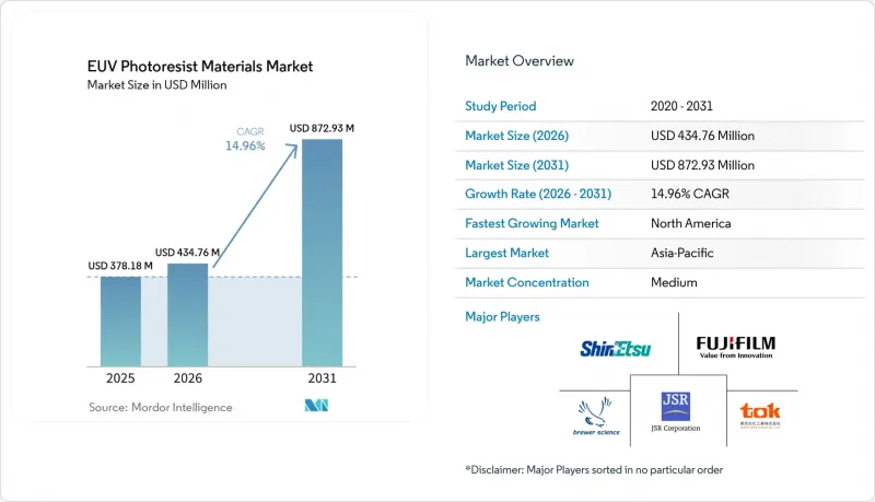
Mordor Intelligence에 의하면, EUV 포토레지스트 재료 시장 규모는 2025년 3억 7,818만 달러로 평가되었고, 2026년 4억 3,476만 달러로 추정되고, 2031년까지 8억 7,293만 달러로 확대될 전망이며, 2026-2031년 연평균 복합 성장률(CAGR)은 14.96%를 나타낼 전망입니다.
본 보고서는 레지스트 유형별(화학 증폭형 레지스트, 금속 산화물 레지스트, 비화학 증폭형 및 드라이 레지스트), 노드 호환성별(최첨단 3nm 이하 및 5nm-7nm의 선진 노드), 최종 고객 유형별(퓨어플레이 파운드리 및 IDM), 지역별(북미, 유럽, 아시아태평양, 기타 지역)로 분류되어 있습니다. 시장 전망은 금액(달러) 기준으로 제시되어 있습니다.
세계의 EUV 포토레지스트 재료 시장 동향 및 분석
3nm 이하 노드에서의 EUV의 급속한 보급
액침 심자외선(DUV) 멀티패터닝에서 단일 패스 극자외선(EUV) 노광으로의 전환을 통해, 첨단 미세 구조의 해상도 한계가 해소됩니다. TSMC는 현재 2나노미터 공정에서 EUV를 사용하여 20층 이상을 패터닝하고 있으며, 이는 3나노미터 공정에서 사용되던 층 수의 거의 2배에 해당하여 마스크의 총 수와 공정 단계를 줄이고 있습니다. 인텔은 8나노미터 해상도를 구현하는 고 NA(개구수) 장비를 도입했으며, 이를 통해 단일 노광으로 패터닝이 가능해져 수율을 향상시키고 결함 밀도를 대폭 낮추고 있습니다. 삼성의 2세대 2나노미터 기술은 레지스트 최적화를 통해 라인 에지 거칠기를 1.5나노미터 미만으로 줄인 결과, 수율이 70%에 달했습니다. 각 고-NA 스캐너의 비용은 약 3억 5,000만 달러이지만, 팹은 멀티패터닝 루프를 제거하고 사이클 타임을 단축함으로써 그 차액을 회수하고 있습니다.
AI 가속기용 파브 생산 능력 확대
2025년에는 인공지능(AI) 칩이 3나노미터 웨이퍼 할당량의 대부분을 차지하게 되었으며, 리드타임은 50주를 넘어섰습니다. NVIDIA 한 회사만으로도 2026년 TSMC의 첨단 패키징 생산량의 절반 이상을 확보하고 있어, 웨이퍼 및 패키지 양쪽 분야에서 EUV 포토레지스트 재료 시장에 대한 수요가 급증하고 있습니다. 애리조나주, 테일러, 오하이오주에서의 생산 능력 확충은 CHIPS법에 따른 보조금과 대출로 총 192억 달러의 지원을 받고 있으며, 팹이 본격적으로 가동되기 전부터 레지스트 수주를 앞당기고 있습니다. 고 NA 스캐너 1대당 연간 200만-300만 달러 상당의 포토레지스트를 소비하기 때문에 장비를 추가로 도입하면 그만큼 재료 소비가 증가하게 됩니다.
EUV 스캐너 공급 부족
ASML은 2025년에 60대를 출하하였고, 2027년에는 80대 이상을 출하할 계획이지만, 파운드리 업체들의 미처리 주문량은 2년 후까지 이어지고 있습니다. 납기 지연이 한 번 발생할 때마다 팹은월최대 1만 5,000장의 웨이퍼를 생산하지 못하게 되고, 운영자는 포토레지스트 구매를 제한할 수밖에 없게 되어, EUV 포토레지스트 재료 시장의 수익에 변동을 초래하고 있습니다. 인텔의 오하이오 복합단지 계획이 7년이나 지연된 주된 원인은 사이클이 길고 납기 기간이 긴 고NA 툴의 납품에 있으며, 이는 장비 공급의 독점이 지역 다각화를 얼마나 저해하고 있는지를 여실히 보여주고 있습니다. 단기적인 공급 부족은 금속 산화물 레지스트와 드라이 레지스트의 가치 제안을 더욱 높여주고 있으며, 이 제품들은 선량 효율을 향상시켜 장비당 처리량을 높여줍니다.
부문별 분석
산화주석 클러스터 기술을 핵심으로 하는 금속 산화물 레지스트 시장은 2031년까지 연평균 성장률(CAGR) 18.4%를 기록하며 가장 강력한 성장세를 보일 것으로 전망됩니다. 2025년 시점에서 팹이 검증된 트랙 호환성과 포지토네 극성을 중시하고 있었기 때문에 화학 증폭형 제품이 여전히 EUV 포토레지스트 재료 시장 규모를 주도하고 있었습니다. 2026년, 램 리서치(Ram Research)가 화학 약품 소비량을 최대 25% 줄이고 20나노미터 미만의 단일 프린트 패턴을 구현하는 기상식 ‘Aether’ 플랫폼을 실증함에 따라, 이 플랫폼의 도입 추세에 변화가 생겼습니다.
화학 증폭형 레지스트는 여전히 규모의 경제성을 유지하고 있지만, 3나노미터 미만의 노드에서 발생하는 확률적 결함으로 인해 각 팹 업체들은 대체 화학 기반 기술의 시범 도입을 불가피하게 하고 있습니다. JSR과 램 리서치는 현재 기상 증착과 무기 감광제를 결합한 하이브리드 워크플로를 제공하고 있으며, 이는 예측 기간 내에 기존의 폴리머 기반 제품을 대체할 가능성이 있는 포지티브 톤 금속 산화물 솔루션으로 가는 길을 제시하고 있습니다. 미국 환경보호청(EPA)과 유럽화학물질청(ECHA)의 규제 조치는 PFAS 함량에 상한선을 설정함으로써 이러한 전환을 가속화하고 있으며, 공급업체들에게 PFAS가 포함되지 않은 금속 산화물 및 건식 제제로의 전환을 촉진하고 있습니다.
지역별 분석
북미에서는 CHIPS법에 따른 인센티브가 TSMC 애리조나, 삼성 테일러, 인텔 오하이오의 3개 메가팹 프로젝트를 가속화함에 따라, 2026년부터 2031년까지 19.2%라는 가장 높은 연평균 성장률(CAGR)을 보일 것으로 전망됩니다. 이 공장들이 가동되면, 총 월간 40만 장 이상의 최첨단 웨이퍼 생산이 추가되어, EUV 포토레지스트 재료 시장의 연간 수요가 1억 5,000만-2억 달러 증가하게 될 것입니다. 포토레지스트에 대한 PFAS 사용 규제는 규정 준수상의 모호함을 해소하고 현지에서의 소재 생산을 촉진합니다.
아시아태평양은 2025년에 37.7%의 점유율을 차지했으며, 계속해서 수익의 주축이 될 것입니다. 이는 대만과 한국이 전 세계 EUV 스캐너의 60% 이상을 보유하고 있기 때문입니다. 현지 공급업체들은 물류 경로가 짧다는 이점을 누리고 있는 반면, 일본의 화학 기업들은 삼성이나 TSMC와의 근접성을 활용하기 위해 평택이나 이바라키에서 생산을 확대되고 있습니다. 해당 지역은 여전히 주도권을 유지하고 있지만, 북미의 생산 능력이 확대됨에 따라 시장 점유율 증가 속도는 완만해질 전망입니다.
유럽은 절대 규모 면에서는 뒤처져 있지만, 2030년까지 지역 내 반도체 시장 점유율을 두 배로 늘리는 것을 목표로 하는 430억 유로 규모의 ‘유럽 칩 법(European Chips Act)’의 혜택을 받고 있습니다. Imec의 루벤 거점과 그 인근에 위치한 JSR의 제조 거점은 독일과 프랑스에 건설될 차세대 고NA 노드를 위한 소재 인증 센터로서의 역할을 수행하고 있습니다. REACH 부속서 XV의 제안에 따라 허용되는 PFAS의 기준치가 명확해졌고, 생산 능력 확충을 승인하는 데 필요한 규제상의 확실성이 제공됨에 따라 공급업체들의 관심이 높아지고 있습니다.
기타 혜택 :
- 엑셀 형식 시장 예측(ME) 시트
- 3개월간의 애널리스트 지원
자주 묻는 질문
목차
제1장 서론
제2장 조사 방법
제3장 주요 요약
제4장 시장 구도
제5장 시장 규모 및 성장 예측
제6장 경쟁 구도
제7장 시장 기회 및 향후 전망
LSH 26.06.24According to Mordor Intelligence, the eUV photoresist materials market size is projected to expand from USD 378.18 million in 2025 and USD 434.76 million in 2026 to USD 872.93 million by 2031, registering a CAGR of 14.96% between 2026 and 2031.

This report is Segmented by Resist Type (Chemically Amplified Resists, Metal Oxide Resists, and Non-Chemically Amplified and Dry Resists), Node Compatibility (Leading Edge 3 Nm and Below, and Advanced Nodes 5 Nm To 7 Nm), End Customer Type (Pure-Play Foundries, and IDMs), and Geography (North America, Europe, Asia-Pacific, and Rest of the World). Market Forecasts are Provided in Terms of Value (USD).
Global EUV Photoresist Materials Market Trends and Insights
Rapid EUV Adoption For <=3 Nm Nodes
The migration from immersion deep-ultraviolet multi-patterning to single-pass extreme-ultraviolet exposure eliminates resolution ceilings at advanced geometries. TSMC now patterns more than 20 layers with EUV on its 2-nanometer process, almost twice the count used at 3-nanometer, which reduces total masks and process steps.Intel integrates high-NA tools that achieve 8-nanometer resolution, enabling single-exposure patterning that boosts yield and slashes defect density. Samsung's second-generation 2-nanometer technology reached 70% yields after resist optimizations cut line-edge roughness below 1.5 nanometers. Although each high-NA scanner costs about USD 350 million, fabs recover the differential by eliminating multi-patterning loops and realizing faster cycle times.
Expansion Of AI Accelerator Fab Capacity
Artificial-intelligence chips consumed most 3-nanometer wafer allocations in 2025, stretching lead times past 50 weeks. NVIDIA alone booked more than half of TSMC's advanced packaging output in 2026, swelling demand for EUV photoresist materials market volumes at both wafer and package levels. Capacity additions in Arizona, Taylor, and Ohio, backed by USD 19.2 billion in combined CHIPS Act grants and loans, pull forward resist orders even before the fabs are fully ramped. With every high-NA scanner absorbing USD 2-3 million of photoresist a year, incremental tool deployments translate directly into material consumption.
Limited EUV Scanner Availability
ASML shipped 60 systems in 2025 and plans just over 80 in 2027, yet foundry order books stretch two years ahead. Each delay deprives a fab of up to 15,000 wafers per month, forcing operators to ration photoresist purchases and injecting revenue volatility into the EUV photoresist materials market. Intel's Ohio complex slipped seven years primarily because of long-cycle high-NA tool deliveries, underscoring how monopoly equipment supply throttles regional diversification. Short-term shortages also amplify the value proposition of metal oxide and dry resists, which raise dose efficiency and stretch throughput per tool.
Other drivers and restraints analyzed in the detailed report include:
- Dominance Of Pure-Play Foundries In Leading-Edge Logic
- Government Subsidies For On-Shore Advanced Nodes
- Line Edge Roughness Challenges Below 3 Nm
For complete list of drivers and restraints, kindly check the Table Of Contents.
Segment Analysis
Metal oxide resists, anchored by tin-oxide cluster technology, are projected to register the strongest growth, advancing at an 18.4% CAGR through 2031. In 2025, chemically amplified products still dominated the EUV photoresist materials market size because fabs favor proven track compatibility and positive-tone polarity. Adoption momentum shifted in 2026 when Lam Research demonstrated its vapor-phase Aether platform that cuts chemical consumption by up to 25% and achieves single-print patterns below 20 nanometers.
Chemically amplified resists retain economies of scale, yet stochastic defects at sub-3-nanometer nodes compel fabs to pilot alternative chemistries. JSR and Lam Research now offer hybrid workflows that pair vapor deposition with inorganic photosensitizers, signaling a path toward positive-tone metal oxide solutions that could displace polymer incumbents within the forecast horizon. Regulatory moves by the U.S. Environmental Protection Agency and the European Chemicals Agency accelerate this pivot by capping PFAS content, incentivizing suppliers to transition to PFAS-free metal oxide and dry formulations.
Geography Analysis
North America is projected to record the fastest CAGR at 19.2% during 2026-2031 as CHIPS Act incentives accelerate three mega-fab projects: TSMC Arizona, Samsung Taylor, and Intel Ohio. Once operational, these plants will collectively add more than 400,000 leading-edge wafer starts per month, translating into an additional USD 150-200 million in annual demand for EUV photoresist materials market volumes. Regulations that establish a controlled-use pathway for PFAS in photoresists reduce compliance ambiguity and encourage local production of materials.
Asia-Pacific remains the revenue anchor, with a 37.7% share in 2025, as Taiwan and South Korea host more than 60% of the global EUV scanner fleet. Local suppliers benefit from short logistics lanes, while Japanese chemical companies are expanding production in Pyeongtaek and Ibaraki to co-locate with Samsung and TSMC. Although the region maintains its leadership, incremental share gains are likely to moderate as North American capacity scales.
Europe trails in absolute size but benefits from the EUR 43 billion European Chips Act, which aims to double the regional semiconductor share by 2030. Imec's Leuven hub and JSR's nearby manufacturing base serve as material qualification centers for future high-NA nodes built in Germany and France. Supplier interest is rising because the REACH Annex XV proposal clarifies permissible PFAS thresholds, providing the regulatory certainty needed to green-light capacity additions.
- JSR Corporation
- Tokyo Ohka Kogyo Co., Ltd. (TOK)
- Fujifilm Holdings Corporation
- Shin-Etsu Chemical Co., Ltd.
- Brewer Science, Inc.
- Inpria Corporation (JSR)
- Merck KGaA (AZ Electronic Materials)
- DuPont de Nemours, Inc.
- Sumitomo Chemical Co., Ltd.
- Dongjin Semichem Co., Ltd.
- Avantama AG
- Lam Research Corporation
- LG Chem Ltd.
- Arkema S.A.
- Tokyo Electron Limited (dry resist co-development)
- S&S Tech Corporation
- Kayaku Advanced Materials, Inc.
- GlobalWafers Co., Ltd.
- Integrated Micro Materials LLC
- Beijing Institute of Chemical Engineering (BICEM)
Additional Benefits:
- The market estimate (ME) sheet in Excel format
- 3 months of analyst support
TABLE OF CONTENTS
1 INTRODUCTION
- 1.1 Study Assumptions and Market Definition
- 1.2 Scope of the Study
2 RESEARCH METHODOLOGY
3 EXECUTIVE SUMMARY
4 MARKET LANDSCAPE
- 4.1 Market Overview
- 4.2 Market Drivers
- 4.2.1 Rapid EUV Adoption for ?3 nm Nodes
- 4.2.2 Dominance of Pure-Play Foundries in Leading-Edge Logic
- 4.2.3 Expansion of AI Accelerator Fab Capacity
- 4.2.4 Government Subsidies for On-shore Advanced Nodes
- 4.2.5 Supply Chain Localization Incentives (CHIPS, K-CHIP, etc.)
- 4.2.6 Yield Gains from Metal Oxide Dry Resists
- 4.3 Market Restraints
- 4.3.1 Line Edge Roughness Challenges Below 3 nm
- 4.3.2 Limited EUV Scanner Availability
- 4.3.3 Environmental Health and Safety Concerns for MOR Chemistries
- 4.3.4 High CoO Compared with Immersion DUV
- 4.4 Industry Value Chain Analysis
- 4.5 Regulatory Landscape
- 4.6 Technological Outlook
- 4.7 Impact of Macroeconomic Factors on the Market
- 4.8 Porter's Five Forces Analysis
- 4.8.1 Bargaining Power of Buyers
- 4.8.2 Bargaining Power of Suppliers
- 4.8.3 Threat of New Entrants
- 4.8.4 Threat of Substitutes
- 4.8.5 Competitive Rivalry
5 MARKET SIZE AND GROWTH FORECASTS (VALUE)
- 5.1 By Resist Type
- 5.1.1 Chemically Amplified Resists (CAR)
- 5.1.2 Metal Oxide Resists (MOR)
- 5.1.3 Non-Chemically Amplified / Dry Resists
- 5.2 By Node Compatibility
- 5.2.1 Leading Edge (3 nm and Below)
- 5.2.2 Advanced Nodes (5 nm-7 nm)
- 5.3 By End Customer Type
- 5.3.1 Pure-Play Foundries
- 5.3.2 IDMs (Integrated Device Manufacturers)
- 5.4 By Geography
- 5.4.1 North America
- 5.4.1.1 United States
- 5.4.1.2 Canada
- 5.4.1.3 Mexico
- 5.4.2 Europe
- 5.4.2.1 United Kingdom
- 5.4.2.2 Germany
- 5.4.2.3 France
- 5.4.2.4 Italy
- 5.4.2.5 Rest of Europe
- 5.4.3 Asia-Pacific
- 5.4.3.1 China
- 5.4.3.2 Japan
- 5.4.3.3 India
- 5.4.3.4 South Korea
- 5.4.3.5 Rest of Asia-Pacific
- 5.4.4 Rest of the World
- 5.4.1 North America
6 COMPETITIVE LANDSCAPE
- 6.1 Market Concentration
- 6.2 Strategic Moves
- 6.3 Market Share Analysis
- 6.4 Company Profiles (includes Global Level Overview, Market Level Overview, Core Segments, Financials as available, Strategic Information, Market Rank/Share, Products and Services, Recent Developments)
- 6.4.1 JSR Corporation
- 6.4.2 Tokyo Ohka Kogyo Co., Ltd. (TOK)
- 6.4.3 Fujifilm Holdings Corporation
- 6.4.4 Shin-Etsu Chemical Co., Ltd.
- 6.4.5 Brewer Science, Inc.
- 6.4.6 Inpria Corporation (JSR)
- 6.4.7 Merck KGaA (AZ Electronic Materials)
- 6.4.8 DuPont de Nemours, Inc.
- 6.4.9 Sumitomo Chemical Co., Ltd.
- 6.4.10 Dongjin Semichem Co., Ltd.
- 6.4.11 Avantama AG
- 6.4.12 Lam Research Corporation
- 6.4.13 LG Chem Ltd.
- 6.4.14 Arkema S.A.
- 6.4.15 Tokyo Electron Limited (dry resist co-development)
- 6.4.16 S&S Tech Corporation
- 6.4.17 Kayaku Advanced Materials, Inc.
- 6.4.18 GlobalWafers Co., Ltd.
- 6.4.19 Integrated Micro Materials LLC
- 6.4.20 Beijing Institute of Chemical Engineering (BICEM)
7 MARKET OPPORTUNITIES AND FUTURE OUTLOOK
- 7.1 White-Space and Unmet-Need Assessment
