|
시장보고서
상품코드
2099467
DRAM 제조용 포토레지스트 및 EUV 포토케미컬 : 시장 점유율 분석, 업계 동향 및 통계, 성장 예측(2026-2031년)Photoresist and EUV Photochemicals For DRAM Manufacturing - Market Share Analysis, Industry Trends & Statistics, Growth Forecasts (2026 - 2031) |
||||||
 Mordor Intelligence
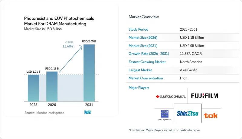
Mordor Intelligence에 의하면, DRAM 제조용 포토레지스트 및 EUV 포토케미컬 시장은 2025년 10억 1,000만 달러로 평가되었습니다. 2026년 11억 8,000만 달러에서 2031년까지 20억 5,000만 달러로 확대되어 2026년부터 2031년에 걸쳐 CAGR 11.68%를 나타낼 것으로 예측됩니다.
본 보고서는 파장(극자외선, ArF 침지, KrF 등), 레지스트 화학(화학 증폭형 레지스트, 금속 산화물 레지스트 등), 레지스트 특성(포지티브 톤 레지스트, 네거티브 톤 레지스트), DRAM 제품 유형(표준 DRAM, 모바일 DRAM 등) 및 지역별로 분류되어 있습니다. 시장 예측은 금액(달러) 기준으로 제시되어 있습니다.
DRAM 제조용 포토레지스트 및 EUV 포토케미컬 시장 동향과 전망
첨단 DRAM 패터닝에서 EUV의 급속한 보급
첨단 DRAM에서 EUV가 제한적인 공정 실험이 아닌 일상적인 생산 도구로 채택됨에 따라, EUV의 급속한 보급은 DRAM 제조용 포토레지스트 및 EUV 포토케미컬 시장의 최대 성장 동력이 되고 있습니다. SK하이닉스는 이미 연속되는 DRAM 세대에 걸쳐 EUV 사용을 확대해 왔으며, 동사의 1c 로드맵에서는 웨이퍼당 최소 5층의 EUV 층으로 전환함에 따라 레지스트 수요는 완만한 증가가 아닌 단계적으로 증가했습니다. 또한, 이 회사는 2025년 9월 청주 DRAM 공장에 고NA EUV 시스템 ‘TWINSCAN EXE,5200B’를 도입했습니다. 이에 따라 소재 공급업체들은 기존보다 더 이른 시점에서 다음 인증 주기를 위한 준비를 서둘러야만 했습니다. 2026년 3월, SK하이닉스는 ASML로부터 11조 9,500억 원(88억 달러)에 EUV 스캐너 30대 이상을 추가로 구매할 계획을 발표했습니다. 납품은 2027년까지 예정되어 있으며, 이 수주량은 인증을 완료한 레지스트 시스템이 필요한 웨이퍼 시작 수량의 지속적인 증가를 시사하는 것이었습니다. 2026년 메모리 고객을 위한 EUV 주문이 사실상 매진됨에 따라, 병목 현상은 장비 수요에서 소재 인증으로 이동하여 이미 인증을 받은 공급업체의 입지를 강화하는 한편, 신규 배합에 대한 단기적인 진입 장벽을 높였습니다. 이 변화가 중요한 이유는 DRAM 제조용 포토레지스트 및 EUV 포토케미컬 시장이 더 이상 팹이 EUV를 원하느냐에 달려 있는 것이 아니라, 승인된 공급업체가 추가되는 각 층에 대응하기 위해 일관된 생산 등급의 화학 물질을 충분히 신속하게 확대 생산할 수 있는지에 달려 있게 되었기 때문입니다.
AI 서버에서 HBM 층 구조의 복잡화
HBM의 복잡화가 진행됨에 따라, DRAM 제조용 포토레지스트 및 EUV 포토케미컬 시장의 품질 가치가 높아지고 있습니다. 이는 AI 서버의 메모리 스택이 주류 DRAM 제품보다 더 엄격한 리소그래피 제어를 필요로 하기 때문입니다. HBM4 스택의 로드맵은 층 수 증가와 상호 연결 구조의 고밀도화로 전환되고 있으며, 이에 따라 각 공정에서의 오버레이, 결함률 및 라인 에지 제어에 대한 민감도가 향상되고 있습니다. 이러한 추세는 공급업체의 경제성에도 변화를 가져오고 있습니다. 왜냐하면 첨단 로직과 첨단 메모리 모두에서 인증을 받은 레지스트 공급업체는 서로 다른 고객 프로그램 간에 일관된 기술적 성능을 유지하면서, 더 대규모의 고부가가치 고객 기반에 개발 비용을 분산시킬 수 있기 때문입니다. 또한 SK하이닉스가 인디애나주 웨스트라파예트에 위치한 HBM 첨단 패키징 시설에 대해 CHIPS법에 근거한 4억 5,800만 달러의 지원을 확보함에 따라 북미의 중요성도 높아졌습니다. 이를 통해 고객 기반 근처에 신뢰성 높은 소재 공급 체계를 필요로 하는 새로운 프리미엄 등급 수요 거점이 창출될 것입니다. 아울러 HBM 생산에서는 수율의 중요성이 더욱 커집니다. 이는 고부가가치 적층 제품의 경우, 결함으로 인한 손실이 표준 범용 DRAM보다 더 큰 비용 부담을 초래하기 때문입니다. 그 결과, DRAM 제조용 포토레지스트 및 EUV 포토케미컬 시장은 HBM을 통해 수량 면에서 확대되고 있을 뿐만 아니라, 단순한 공급량보다 성능과 결함 관리가 더욱 중시되는 가격 구조로 전환되고 있습니다.
새로운 레지스트 화학 조성에 대한 DRAM 팹의 긴 인증 주기
DRAM 제조용 포토레지스트 및 EUV 포토케미컬 시장에서 긴 인증 주기는 여전히 가장 심각한 내부 제약 요인으로 남아 있습니다. 이는 기술적으로 유망한 소재라 하더라도 양산 도입 전에 장기간에 걸친 웨이퍼 상의 검증이 필요하기 때문입니다. 이 문제는 MOR이나 PFAS 프리 CAR와 같은 새로운 화학 조성에서 특히 두드러지며, 실험실에서의 결과가 양호하더라도 DRAM 양산으로의 신속한 전환이 보장되는 것은 아닙니다. 노광 장비, 트랙, 베이킹 조건, 현상액, 결함 맵, 수율 윈도우에 걸쳐 공정 통합 검증이 필요하며, 공급업체가 안정적인 상업적 수익을 확보하기까지 시간과 비용이 모두 증가합니다. 그 결과, 이미 고객의 공정 흐름에 통합된 기존 공급업체에게는 구조적 우위가 생깁니다. 왜냐하면 첨단 노드에서의 조성 변경은 매번 추가적인 공정 검증과 사내 승인 절차를 필요로 하기 때문입니다. 이로 인해 DRAM 제조용 포토레지스트 및 EUV 포토케미컬 시장 점유율 변동이 둔화되며, 신규 진출기업이 기술적 진보를 수요 상황이 시사하는 만큼 신속하게 상업적 매출로 전환하는 것을 방해하고 있습니다. 또한, 자본력을 바탕으로 한 기존 공급업체가 여러 세대의 DRAM에 걸쳐 수익화 이전의 개발 비용을 흡수하는 측면에서 여전히 신규 진출기업보다 유리한 입장에 있는 이유도 여기에 설명되어 있습니다.
부문 분석
2025년, DRAM 제조용 포토레지스트 및 EUV 포토케미컬 시장의 파장 부문에서 ArF 침지 방식이 61.54%를 차지했으며, 이러한 탄탄한 기반을 바탕으로 상업적으로 생산되는 대부분의 DRAM 층에서 포토레지스트 수요의 중심적인 위치를 계속 차지했습니다. 2025년, DRAM 제조용 포토레지스트 및 EUV 포토케미컬 시장에서 ArF 침지 공정은 61.54%를 차지했으며, 이는 웨이퍼 공정의 광범위한 분야에서 여전히 주류를 이루고 있는 반복 패터닝 공정에서 해당 기술이 수행하는 역할을 반영합니다. 그 이유는 실용적인 데 있습니다. DRAM 제조업체들은 여전히 여러 층에 걸쳐 SAQP 및 관련 멀티 패터닝 기법에 의존하고 있으며, 이 분야에서 ArFi는 여전히 비용 효율성이 뛰어나고 운영 면에서도 익숙하기 때문입니다. 이러한 도입 기반 덕분에, 더 중요한 층이 EUV로 전환되고 있는 상황에서도 ArFi의 출하량은 견조한 추세를 유지하고 있으며, 기존 대량 생산용 레지스트 수요가 급격히 감소하는 것을 막고 있습니다. DRAM 제조용 포토레지스트 및 EUV 포토케미컬 업계에서는 이로 인해 이중적인 공급 수요가 발생하고 있습니다. 즉, 팹은 계속해서 대량의 ArFi를 구매하는 한편, 인증된 EUV 소재에 대한 의존도도 높이고 있는 것입니다. 따라서 폭넓은 제품 포트폴리오를 보유한 공급업체는 좁은 분야에 특화된 전문 업체보다 유리한 입장에 있습니다. 왜냐하면 현재의 생산을 뒷받침하면서 동시에 미래 층을 위한 인증 작업을 진행할 수 있기 때문입니다.
EUV는 가장 빠르게 성장하는 파장 부문으로, 2031년까지 연평균 성장률(CAGR)이 12.67%를 나타낼 것으로 예측됩니다. 이는 첨단 DRAM 로드맵 전반에 걸쳐 EUV 층 수가 꾸준히 증가하고 있음을 반영합니다. Samsung Electronics와 SK하이닉스는 2026년 초까지 이미 의미 있는 고NA EUV 공정 기반을 구축했으며, 이를 통해 레지스트 공급업체들은 다음 단계의 인증 및 공정 조정을 위한 보다 명확한 기반을 확보할 수 있었습니다. JSR과 임프리아 역시 저 NA 및 고 NA EUV 용도를 위한 포지티브 톤 및 네거티브 톤 MOR 시스템 모두에서 진전을 보고하고 있으며, 이는 소재 개발이 스캐너 준비에 뒤처지지 않고 병행하여 진행되고 있음을 보여줍니다. 실질적인 영향으로, DRAM 제조용 포토레지스트 및 EUV 포토케미컬 시장에서 EUV의 성장은 웨이퍼 전체에 대한 ArFi 사용의 단순한 대체가 아니라, 층의 추가에 의해 이루어지고 있습니다. 이로 인해 웨이퍼당 총 재료 사용량은 계속 증가하고 있습니다. DRAM 노드에서는 새로운 EUV 기회가 추가되고 있는 반면, 비용 및 공정상의 이유로 DRAM 제조용 포토레지스트 및 EUV 포토케미컬 시장에서 ArFi를 많이 사용하는 층이 여전히 몇 개 남아 있기 때문입니다.
2025년, DRAM 제조용 포토레지스트 및 EUV 포토케미컬 시장에서 화학 증폭형 레지스트는 80.12%의 점유율을 차지했습니다. 이러한 우위는 ArFi 및 현재의 EUV 이용 사례 양쪽에 걸쳐 수십 년에 걸친 공동 개발, 공정에 대한 숙련도, 그리고 임베디드 인증의 성과를 반영한 것입니다. 2025년, 화학 증폭형 레지스트는 포토레지스트 및 EUV 포토케미컬 시장의 80.12%를 차지하며, DRAM 팹에서 이미 사용되고 있는 기존 트랙 시스템, 반사 방지층 및 현상액과의 깊은 통합을 뒷받침했습니다. 레지스트의 화학 조성을 변경하는 것은 단순히 코팅용 병에 영향을 미칠 뿐만 아니라, 주변 공정 스택 및 고객 측의 인증 부담에도 영향을 미치기 때문에 이러한 확고한 입지를 뒤집기는 어렵습니다. 스미토모 화학과 듀폰은 첨단 리소그래피용 CAR 개발을 지속적으로 추진하고 있으며, 듀폰의 Qnity 팀은 2025년 SPIE에서 ArF 레지스트용 PFAS 대체재에 관한 연구 성과를 발표했습니다. 이는 기존 화학 계열이 정체된 것이 아니라 여전히 진화하고 있음을 보여줍니다. 이는 DRAM 제조용 포토레지스트 및 EUV 포토케미컬 시장에 중요한 의미를 지닙니다. 왜냐하면 CAR는 여전히 더 새로운 화학 플랫폼으로의 전환을 자금 면에서 뒷받침하는 양산 기반으로 남아 있기 때문입니다. 또한 이는 고객들이 실적이 부족한 소재 계열로 공정의 대부분을 전환하기 전에, 여러 단계에서 더 깨끗하고 규제를 준수하는 CAR 배합을 우선적으로 채택할 가능성이 높다는 것을 의미합니다.
DRAM 제조용 포토레지스트 및 EUV 포토케미컬 시장에서 금속 산화물 레지스트는 가장 빠르게 성장하는 화학 부문으로, 2026년부터 2031년까지 연평균 성장률(CAGR) 13.07%를 기록했습니다. 이는 EUV 광자의 흡수율이 높고 처리량 특성이 개선되었기 때문입니다. Imec은 2026년 2월, 산소가 풍부한 노광 후 베이킹 환경을 통해 MOR의 감광 속도가 15-20% 향상되었음을 보여주었습니다. 이로 인해 EUV 조건 하에서의 노광 선량 요건이 직접적으로 감소하여 스캐너의 생산성이 향상되었습니다. 이 결과는 처리량이 MOR 보급의 주요 장벽 중 하나였습니다는 점에서 중요하며, 노광 선량의 감소는 비용이 높은 첨단 노드에서 이 소재의 채택을 촉진하는 요인이 될 것입니다. 또한, 2026년 5월 JSR이 엔테그리스(Entegris)사와 체결한 교차 라이선스 계약은 MOR을 둘러싼 경쟁이 화학 분야에 그치지 않고, 전구체 합성, 여과 및 청정 공급 인프라로 확대되고 있음을 보여주었습니다. SPIE 2025를 통해 발표된 IBM의 조사는 첨단 제조 요구와 관련된 미세 피치에서 하드웨어 지원에 의한 MOR 패터닝의 진전을 보여줌으로써 이러한 추세를 더욱 뒷받침했습니다. DRAM 제조용 포토레지스트 및 EUV 포토케미컬 시장에서 MOR은 현재로서는 여전히 CAR보다 시장 규모가 작지만, 그 성장세는 더 이상 단순한 이론적 가능성에 그치지 않고 측정 가능한 공정상의 이점으로 뒷받침되고 있습니다.
지역별 분석
2025년, DRAM 제조용 포토레지스트 및 EUV 포토케미컬 시장에서 아시아태평양이 88.42%를 차지했습니다. 이는 한국, 일본, 대만의 DRAM 웨이퍼 생산과 레지스트 제조 능력 간의 밀접한 연관성을 반영한 것입니다. 2025년, 아시아태평양은 DRAM 제조용 포토레지스트 및 EUV 포토케미컬 시장의 88.42%를 차지하며, 이 지역은 소비와 공급 양면에서 명실상부한 중심지가 되었습니다. 한국은 Samsung Electronics와 SK하이닉스가 계속해서 최첨단 DRAM 생산과 EUV에 대한 선제 투자를 주도함에 따라 최대의 국내 수요 기반국으로 자리매김했습니다. SK하이닉스는 2026년 3월, 2027년까지 11조 9,500억 원(88억 달러) 규모의 EUV 스캐너 구매 계획을 발표하며 이러한 전망을 더욱 공고히 했습니다. 이를 통해 인증된 소재에 대한 장기적인 수요 파이프라인이 뒷받침되었습니다. 공급 측면에서도 일본은 그 중요성을 유지했습니다. TOK, JSR, 신에츠 화학공업, 스미토모 화학, 후지필름이 반도체 소재에 관한 긴밀한 연구개발·생산 네트워크를 지속적으로 운영하고 있으며, 여기에는 신에츠 화학공업의 이세사키에서의 새로운 국내 투자도 포함됩니다.
북미는 가장 성장세가 두드러진 지역으로, 2026년부터 2031년까지 연평균 성장률(CAGR) 12.56%를 기록했습니다. 이는 기존의 생산 능력 갱신 주기가 아닌, DRAM 제조 투자의 새로운 단계를 반영한 것입니다. 최대 64억 달러 규모의 CHIPS 지원을 받은 마이크론의 아이다호주 및 뉴욕주 프로젝트는 해당 지역의 국내 메모리 소재 수요에 대한 장기적인 전망을 가장 견고하게 만들었습니다. 또한 SK하이닉스는 인디애나주에서 4억 5,800만 달러의 지원을 받은 HBM 패키징 프로젝트를 통해 프리미엄 수요원을 추가했습니다. 한편, 삼성의 텍사스주 투자는 미국 내 반도체 소재의 비즈니스 기회를 더욱 확대시켰습니다. 이러한 새로운 설비 확장이 중요하게 여겨지는 이유는 북미의 DRAM 제조용 포토레지스트 및 EUV 포토케미컬 시장이 기존의 생산 능력보다는 국내 인증 요건, PFAS(퍼플루오로알킬 물질)에 대한 면밀한 검토, 그리고 공급망 추적성 요건에 의해 형성되고 있기 때문입니다.
유럽 시장 점유율은 미미했으나, 이 지역의 영향력은 DRAM 웨이퍼의 직접적인 생산량보다는 공정 개발을 통해 발휘되었기 때문에 전략적으로 중요한 위치를 계속 차지하고 있었습니다. 벨기에 Imec의 NanoIC 및 EUV 연구 프로그램은 레지스트의 공동 개발을 지속적으로 지원하고 있으며, 해당 연구소가 2026년 2월에 발표한 MOR 연구 결과에 따르면 산소가 풍부한 노출 후 소성(PEB) 조건에서 감광 속도가 15-20% 향상된 것으로 나타났습니다. 이를 통해 유럽은 세계 DRAM 생산량에서 동등한 점유율을 차지하지 못함에도 불구하고, 차세대 리소그래피 기술 준비를 추진하는 데 있어 매우 큰 역할을 수행했습니다. 세계 기타 지역의 경우, 주요 클러스터 이외에서 계획되고 있는 신규 팹 건설 계획이 DRAM 제조용 포토레지스트 및 EUV용 광화학약품 시장의 단기적인 구매 패턴을 실질적으로 변화시키는 데 필요한 규모에 아직 미치지 못했기 때문에 현재 DRAM용 포토레지스트 수요에서는 무시할 수 있는 수준에 그쳤습니다.
기타 혜택 :
- 엑셀 형식 시장 예측(ME) 시트
- 3개월간의 애널리스트 지원
자주 묻는 질문
목차
제1장 서론
제2장 조사 방법
제3장 주요 요약
제4장 시장 구도
제5장 시장 규모 및 성장 예측
제6장 경쟁 구도
제7장 시장 기회 및 향후 전망
KTH 26.08.10According to Mordor Intelligence, the photoresist and EUV photochemicals market for DRAM manufacturing size is projected to expand from USD 1.01 billion in 2025 and USD 1.18 billion in 2026 to USD 2.05 billion by 2031, registering a CAGR of 11.68% between 2026 and 2031.
This report is Segmented by Wavelength (Extreme Ultraviolet, Arf Immersion, Krf, and More), Resist Chemistry (Chemically Amplified Resists, Metal-Oxide Resists, and More), Resist Tone (Positive Tone Resists, and Negative Tone Resists), DRAM Product Type (Standard DRAM, Mobile DRAM, and More), and Geography. The Market Forecasts are Provided in Terms of Value (USD).
Insights and Trends of Photoresist and EUV Photochemicals Market For DRAM Manufacturing
Rapid EUV Adoption in Advanced DRAM Patterning
Rapid EUV adoption has become the strongest growth engine in the photoresist and EUV photochemicals Market for DRAM manufacturing, as advanced DRAM now uses EUV as a recurring production tool rather than a limited process experiment. SK hynix had already expanded EUV use across successive DRAM generations, and its 1c roadmap moved to at least 5 EUV layers per wafer, which raised resist demand in a stepwise manner rather than gradually. The company also installed a TWINSCAN EXE:5200B high-NA EUV system at its Cheongju DRAM fab in September 2025, which pushed material suppliers to prepare for the next qualification cycle earlier than before. In March 2026, SK hynix disclosed a plan to buy more than 30 additional EUV scanners from ASML for KRW 11.95 trillion (USD 8.8 billion), with deliveries scheduled through 2027, and that order volume pointed to a sustained rise in wafer starts requiring qualified resist systems. Once memory customer EUV orders for 2026 were effectively sold out, the bottleneck shifted from tool demand to materials qualification, strengthening the position of suppliers already qualified and raising the near-term entry barrier for new formulations. This shift matters because the photoresist and EUV photochemicals Market for DRAM manufacturing now depends less on whether fabs want EUV and more on whether approved suppliers can scale consistent, production-grade chemistry fast enough to support each added layer.
Rising HBM Layer Complexity In AI Servers
Rising HBM complexity is lifting the quality value of the photoresist and EUV photochemicals Market for DRAM manufacturing, because AI server memory stacks demand tighter lithography control than mainstream DRAM products. HBM4 stack roadmaps are moving to higher layer counts and denser interconnect structures, and that raises sensitivity to overlay, defectivity, and line-edge control across each processing step. That pattern changes supplier economics, because a resist vendor qualified in both advanced logic and advanced memory can spread development costs across larger, high-value accounts while maintaining consistent technical performance across different customer programs. North America also became more relevant when SK hynix secured USD 458 million in CHIPS support for its HBM advanced packaging facility in West Lafayette, Indiana, creating a new premium-grade demand node that will require dependable material support close to its customer base. HBM production also makes yield more valuable, because defect losses carry a larger cost penalty on high-value stacked products than on standard commodity DRAM. As a result, the photoresist and EUV photochemicals market is not only expanding in volume through HBM, it is also moving toward a pricing structure where performance and defect control matter more than simple volume supply.
Long DRAM Fab Qualification Cycles For New Resist Chemistries
Long qualification cycles remain the most serious internal restraint on the photoresist and EUV photochemicals market for DRAM manufacturing, because technically promising materials still need extended on-wafer validation before any volume rollout. The problem is especially visible for newer chemistries such as MOR and PFAS-free CAR, where even a favorable lab result does not guarantee a fast transfer into DRAM mass production. Process integration must be checked across exposure tools, tracks, bake conditions, developers, defect maps, and yield windows, and that raises both time and cost before a supplier can secure stable commercial revenue. The result is a structural advantage for incumbent vendors that already sit inside customer flows, because every formulation change at advanced nodes can trigger additional process checks and internal approval cycles. That slows down share shifts in the photoresist and EUV photochemicals Market for DRAM manufacturing and keeps novel entrants from converting technical progress into commercial sales as quickly as demand conditions might suggest. It also explains why capital-backed incumbents are still better positioned than challengers to absorb pre-revenue development costs over multiple DRAM generations.
Other drivers and restraints analyzed in the detailed report include:
- Multi-Patterning Demand for ArFi in Mature DRAM Layers
- Government Fab Incentives for Local Memory Capacity
- EUV Tool Bottlenecks Slowing Material Ramp Rates
For complete list of drivers and restraints, kindly check the Table Of Contents.
Segment Analysis
ArF immersion held 61.54% of the wavelength segment of photoresist and EUV photochemicals market for DRAM manufacturing in 2025, and that large base kept it at the center of photoresist demand across most commercially produced DRAM layers. ArF immersion accounted for 61.54% of the photoresist and EUV photochemicals market for DRAM manufacturing in 2025, reflecting its role in repeated patterning flows that still dominate broad sections of the wafer process. The reason is practical, because DRAM makers still rely on SAQP and related multi-patterning methods across several layers, where ArFi remains cost-effective and operationally familiar. That installed base keeps ArFi volume resilient even as more critical layers shift toward EUV, and it prevents a rapid collapse in legacy high-volume resist demand. In the photoresist and EUV photochemicals industry, this creates a dual-track supply need where fabs continue buying large ArFi volumes while also increasing their dependence on qualified EUV materials. Suppliers with broad portfolios, therefore, remain better placed than narrow specialists, because they can support current production while qualifying future layers in parallel.
EUV was the fastest-growing wavelength segment, with a 12.67% CAGR through 2031, reflecting a steady increase in EUV layer counts across advanced DRAM roadmaps. Samsung and SK hynix had already built a meaningful high-NA EUV process base by early 2026, which gave resist vendors a clearer platform for next-step qualification and process tuning. JSR and Inpria also documented progress on both positive-tone and negative-tone MOR systems for low-NA and high-NA EUV applications, which shows that materials development is now moving alongside scanner preparation rather than trailing it. The practical effect is that EUV growth in the photoresist and EUV photochemicals Market for DRAM manufacturing is coming from layer additions rather than simple replacement of ArFi use across the whole wafer. That keeps total material intensity per wafer moving upward, because DRAM nodes are adding new EUV opportunities while still holding on to several ArFi-intensive layers for cost and process reasons in the photoresist and EUV photochemicals market for DRAM manufacturing.
Chemically amplified resists held 80.12% share of photoresist and EUV photochemicals market for DRAM manufacturing in 2025, and that lead reflected decades of co-development, process familiarity, and embedded qualification across both ArFi and current EUV use cases. Chemically amplified resists accounted for 80.12% of the photoresist and EUV photochemicals market in 2025, underscoring their deep integration with established track systems, anti-reflective layers, and developer chemistry already used in DRAM fabs. That installed position is difficult to displace because switching the resist chemistry does not affect only the coating bottle; it also affects the surrounding process stack and the customer qualification burden. Sumitomo Chemical and DuPont have continued to advance CAR development for advanced lithography, and DuPont's Qnity team presented work on PFAS alternatives for ArF resist at SPIE in 2025, demonstrating that incumbent chemistry families are still evolving rather than standing still. This matters for the photoresist and EUV photochemicals market because CAR remains the volume foundation that funds the transition into newer chemistry platforms. It also means customers are likely to adopt cleaner or more compliant CAR formulations first across many layers before shifting larger shares of flow to less-proven material classes.
Metal-oxide resists were the fastest-growing chemistry segment, of the photoresist and EUV photochemicals market for DRAM manufacturing, at a 13.07% CAGR over 2026-2031, driven by their stronger EUV photon absorption and their improving throughput profile. Imec showed in February 2026 that an oxygen-enriched post-exposure bake environment improved MOR photo-speed by 15-20%, which directly reduced dose needs and improved scanner productivity under EUV conditions. That result mattered because throughput has been one of the main barriers to wider MOR use, and any dose reduction makes the material case stronger at expensive advanced nodes. JSR's May 2026 cross-licensing agreement with Entegris also showed that MOR competition is moving beyond chemistry alone and into precursor synthesis, filtration, and clean delivery infrastructure. IBM research presented through SPIE 2025 added further support by showing hardware-assisted MOR patterning progress at fine pitches relevant to advanced manufacturing needs. In the photoresist and EUV photochemicals market, MOR is still smaller than CAR today, but its momentum is now tied to measurable process gains rather than to only theoretical promise.
Complete Report Scope:
- By Wavelength
- Extreme Ultraviolet (EUV)
- ArF Immersion (ArFi)
- KrF
- I-Line/G-Line
- By Resist Chemistry
- Chemically Amplified Resists (CAR)
- Metal-Oxide Resists (MOR)
- Non-CAR Organic Resists
- By Resist Tone
- Positive Tone Resists
- Negative Tone Resists
- By DRAM Product Type
- Standard DRAM
- Mobile DRAM (LPDDR)
- Graphics DRAM (GDDR)
- High Bandwidth Memory (HBM)
- Server DRAM
- Other DRAM Product Types
- By Geography
- North America
- Europe
- Asia-Pacific
- China
- Japan
- South Korea
- Taiwan
- Rest of Asia-Pacific
- Rest of the World
Geography Analysis
Asia-Pacific accounted for 88.42% of thephotoresist and EUV photochemicals market for DRAM manufacturing industry in 2025, reflecting the close link between DRAM wafer production and resist manufacturing capacity in South Korea, Japan, and Taiwan. Asia-Pacific accounted for 88.42% of the photoresist and EUV photochemicals market in 2025, making the region the clear center of both consumption and supply. South Korea remained the largest national demand base because Samsung Electronics and SK Hynix continued to anchor advanced DRAM output and forward EUV investment. SK hynix strengthened that outlook in March 2026 when it disclosed its KRW 11.95 trillion (USD 8.8 billion) EUV scanner purchase plan through 2027, which supported a longer visible demand pipeline for qualified materials. Japan remained just as important on the supply side, as TOK, JSR, Shin-Etsu Chemical, Sumitomo Chemical, and Fujifilm continued to operate dense R&D and production networks for semiconductor materials, including new domestic investment from Shin-Etsu in Isesaki.
North America was the fastest-growing geography, with a 12.56% CAGR over 2026-2031, reflecting a new phase of DRAM manufacturing investment rather than a typical capacity refresh cycle. Micron's Idaho and New York projects, backed by up to USD 6.4 billion in CHIPS support, created the strongest long-term case for domestic memory materials demand in the region. SK hynix also added a premium demand point through its USD 458 million supported HBM packaging project in Indiana, while Samsung's Texas investment widened the broader semiconductor materials opportunity across the United States. This new build-out matters because the photoresist and EUV photochemicals market in North America is being shaped by domestic qualification, PFAS scrutiny, and supply chain traceability requirements more than by legacy installed capacity.
Europe held a modest share, but it remained strategically important because much of the region's influence came through process development rather than through direct DRAM wafer volume. Imec's NanoIC and EUV research programs in Belgium continued to support resist co-development, and the institute's February 2026 MOR work showed a 15-20% photo-speed improvement under oxygen-enriched post-exposure bake conditions. That gave Europe an outsized role in advancing next-generation lithography readiness even without a comparable share of global DRAM output. The Rest of the World remained negligible for current DRAM photoresist demand, because emerging fab plans outside the main clusters have not yet reached the scale needed to materially change near-term purchasing patterns in the photoresist and EUV photochemicals market for DRAM manufacturing.
- Tokyo Ohka Kogyo Co., Ltd.
- JSR Corporation
- Shin-Etsu Chemical Co., Ltd.
- FUJIFILM Holdings Corporation
- Sumitomo Chemical Co., Ltd.
- DuPont de Nemours, Inc.
- Merck KGaA
- Dongjin Semichem Co., Ltd.
- Brewer Science, Inc.
- Inpria Corporation
- Lam Research Corporation
- Allresist GmbH
- micro resist technology GmbH
- Microchemicals GmbH
- Eternal Materials Co., Ltd.
- Jiangsu Nata Opto-electronic Material Co., Ltd.
- Hubei Dinglong Co., Ltd.
- S&S Tech Corporation
Additional Benefits:
- The market estimate (ME) sheet in Excel format
- 3 months of analyst support
TABLE OF CONTENTS
1 INTRODUCTION
- 1.1 Study Assumptions and Market Definition
- 1.2 Scope of the Study
2 RESEARCH METHODOLOGY
3 EXECUTIVE SUMMARY
4 MARKET LANDSCAPE
- 4.1 Market Overview
- 4.2 Market Drivers
- 4.2.1 Rapid EUV Adoption in Advanced DRAM Patterning
- 4.2.2 Rising HBM Layer Complexity In AI Servers
- 4.2.3 Multi-Patterning Demand for ArFi In Mature DRAM Layers
- 4.2.4 Government Fab Incentives for Local Memory Capacity
- 4.2.5 PFAS-Free Reformulation Pull In Semiconductor Materials
- 4.2.6 Dry Resist and Metal-Oxide Throughput Gains
- 4.3 Market Restraints
- 4.3.1 Long DRAM Fab Qualification Cycles for New Resist Chemistries
- 4.3.2 EUV Tool Bottlenecks Slowing Material Ramp Rates
- 4.3.3 High Purity and Defectivity Requirements Raising Cost of Entry
- 4.3.4 Export Controls and Raw Material Concentration Risk
- 4.4 Industry Value Chain Analysis
- 4.5 Regulatory Landscape
- 4.6 Technological Outlook
- 4.7 Impact of Macroeconomic Factors on the Market
- 4.8 Porter's Five Forces Analysis
- 4.8.1 Threat of New Entrants
- 4.8.2 Bargaining Power of Buyers
- 4.8.3 Bargaining Power of Suppliers
- 4.8.4 Threat of Substitutes
- 4.8.5 Industry Rivalry
5 MARKET SIZE AND GROWTH FORECASTS (VALUE)
- 5.1 By Wavelength
- 5.1.1 Extreme Ultraviolet (EUV)
- 5.1.2 ArF Immersion (ArFi)
- 5.1.3 KrF
- 5.1.4 I-Line/G-Line
- 5.2 By Resist Chemistry
- 5.2.1 Chemically Amplified Resists (CAR)
- 5.2.2 Metal-Oxide Resists (MOR)
- 5.2.3 Non-CAR Organic Resists
- 5.3 By Resist Tone
- 5.3.1 Positive Tone Resists
- 5.3.2 Negative Tone Resists
- 5.4 By DRAM Product Type
- 5.4.1 Standard DRAM
- 5.4.2 Mobile DRAM (LPDDR)
- 5.4.3 Graphics DRAM (GDDR)
- 5.4.4 High Bandwidth Memory (HBM)
- 5.4.5 Server DRAM
- 5.4.6 Other DRAM Product Types
- 5.5 By Geography
- 5.5.1 North America
- 5.5.2 Europe
- 5.5.3 Asia-Pacific
- 5.5.3.1 China
- 5.5.3.2 Japan
- 5.5.3.3 South Korea
- 5.5.3.4 Taiwan
- 5.5.3.5 Rest of Asia-Pacific
- 5.5.4 Rest of the World
6 COMPETITIVE LANDSCAPE
- 6.1 Market Concentration
- 6.2 Strategic Moves
- 6.3 Market Share Analysis
- 6.4 Company Profiles (includes Global Level Overview, Market Level Overview, Core Segments, Financials as available, Strategic Information, Market Rank/Share, Products and Services, Recent Developments)
- 6.4.1 Tokyo Ohka Kogyo Co., Ltd.
- 6.4.2 JSR Corporation
- 6.4.3 Shin-Etsu Chemical Co., Ltd.
- 6.4.4 FUJIFILM Holdings Corporation
- 6.4.5 Sumitomo Chemical Co., Ltd.
- 6.4.6 DuPont de Nemours, Inc.
- 6.4.7 Merck KGaA
- 6.4.8 Dongjin Semichem Co., Ltd.
- 6.4.9 Brewer Science, Inc.
- 6.4.10 Inpria Corporation
- 6.4.11 Lam Research Corporation
- 6.4.12 Allresist GmbH
- 6.4.13 micro resist technology GmbH
- 6.4.14 Microchemicals GmbH
- 6.4.15 Eternal Materials Co., Ltd.
- 6.4.16 Jiangsu Nata Opto-electronic Material Co., Ltd.
- 6.4.17 Hubei Dinglong Co., Ltd.
- 6.4.18 S&S Tech Corporation
7 MARKET OPPORTUNITIES AND FUTURE OUTLOOK
- 7.1 White-Space and Unmet-Need Assessment